I. INTRODUCTION
Either at the mobile terminal or at the satellite level, recent and future telecommunication systems need to integrate several frequency bands into a single terminal. To minimize its bulk, its weight and its cost, a solution consists in using an N-band radio frequency front-end instead of N single band ones. Moreover, these systems would have to be reconfigurable in order to be able to adapt easily to new uses, standard modifications, user numbers, etc. The importance of passive bandpass filters in these front-ends is at the origin of the research presented in this paper.
Over the last few years, a lot of work has been presented regarding passive multi-band bandpass filters. Most of them concern bi-band filters [Reference Quendo, Rius and Person1–Reference Liu, Huang and Wu7], some other ones tri-band [Reference Huang, Wen and Liu8–Reference Jankovic, Geschke and Crnojevic-Bengin11], or quad-band filters [Reference Wu and Yang12, Reference Kuo, Li, Cheng and Chang13], and several works also report on more general methods or synthesis allowing the design of multi-band filters [Reference Quendo, Manchec, Clavet, Rius, Favennec and Person14–Reference Chen, Huang, Horng and Wu18].
To increase the flexibility of such filters, some recent works add reconfiguration to these structures [Reference Zhang and Xue19–Reference Chaudhary, Jeong and Lim23]. These solutions are mainly based on resonators loaded in their center or in their ends with varactor diodes. According to the localization of the diodes and the complexity of the structure, the reconfigurable filters allow the central frequency of only one band to be controlled [Reference Zhang and Xue19–Reference Abunjaileh and Hunter21], the central frequency of all bands to be simultaneously tuned with constant absolute bandwidths [Reference Zhao22], or both the central frequency and the bandwidth of each band to be independently controlled [Reference Chaudhary, Jeong and Lim23, Reference Fourn, Quendo, Rius, Pothier, Blondy, Champeaux, Orlianges, Catherinot, Tanne, Person and Huret24]. Nevertheless, the proposed solutions only concern dual-band filters.
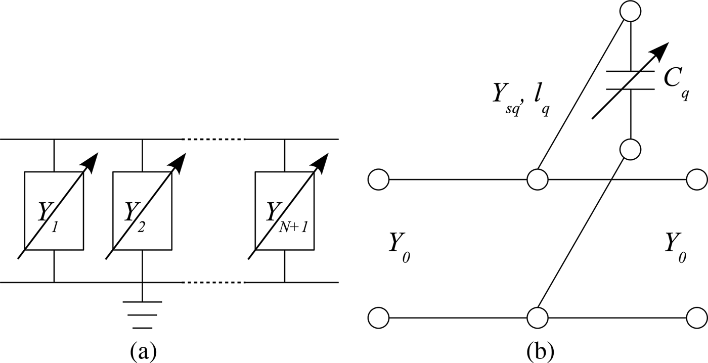
This paper proposes a general method to develop an N-band tunable resonator (cf. Fig. 1(a)). It is based on the association of an N-band dual-behavior resonator (DBR) and tunable capacitors. In fact, it is a generalization of the works presented in [Reference Fourn, Quendo, Rius, Pothier, Blondy, Champeaux, Orlianges, Catherinot, Tanne, Person and Huret24] concerning a mono-band tunable DBR resonator. As described in [Reference Quendo, Manchec, Clavet, Rius, Favennec and Person14], an N-band DBR consists of the parallel association of different N + 1 bandstop structures. One can then obtain N + 1 transmission zeros and N resonances by constructive recombinations. We chose this multi-band resonator topology because each bandstop structure controls a transmission zero independently of the N other ones. It is therefore relatively easy to reconfigure the multi-band resonator in term of resonant frequencies by independently modifying the position of each transmission zero. The realization of a tunable multi-band filter (i.e., involving at least two tunable multi-band resonators) will also allow the bandwidth to be easily controlled due to the presence of multiple transmission zeros between two successive pass bands. Note that this resonator can also be considered as a tunable notch resonator with N + 1 stop bands.

Fig. 1. General scheme of an N-band tunable DBR (a) and description of a bandstop structure (b).
In the case presented here, each bandstop element consists of a stub terminated by a capacitor (cf. Fig. 1(b)) For instance, Fig. 2 gives the electrical response of an ideal eight-band resonator achievable by using nine bandstop structures. As each of them independently fixes a transmission zero, the use of tunable capacitors allows the independent control of each zero and consequently, the resonator response can be easily modified.
Fig. 2. Initial electrical response of an ideal transmission line eight-band tunable resonator.
The main difficulty here is the initial dimensioning of the structure due to its numerous parameters and the integration of the capacitances. The latter are generally integrated after a first dimensioning of a passive structure involving a long and difficult optimization work. The general synthesis of an N-band tunable resonator reported here (Section II) simplifies this since it takes into account these capacitances from the beginning. Indeed, this synthesis directly gives the parameters of the N + 1 bandstop structures, i.e. the length and the impedance of the stubs and the initial value of the capacitors. Section III will demonstrate how one can then easily tune the different bands by varying the values of the capacitors in the case of a tri-band resonator. Section IV will validate the proposed concept with the implementation of this tri-band tunable resonator in microstrip technology. Experimental results are then discussed.
II. RESONATOR SYNTHESIS
The general synthesis presented here allows the development of an N-band tunable resonator to be simplified. After introducing the general equations linked to resonances and transmission zeros, the equations system will be solved in the case of bandstop structures consisting of a stub terminated by a capacitor (cf. Fig. 1).
As for a passive N-band DBR [Reference Quendo, Manchec, Clavet, Rius, Favennec and Person14], the parallel association of N + 1 tunable bandstop structures defined by their frequency-dependent admittance Y q(f) leads to the creation of N + 1 transmission zeros defined by:
 $$Y_q \lpar f_{zq} \rpar \to \infty\comma \; \quad {\rm for}\quad q = 1\comma \; 2\comma \; \ldots\comma \; N + 1\comma \;$$
where f zq are the frequencies of the N + 1 transmission zeros. N resonances are then obtained by considering the constructive recombination criteria which follows:
 $$\sum\limits_{q = 1}^{N + 1} Y_q \lpar f_{0p} \rpar = 0\comma \; \quad {\rm for}\quad p = 1\comma \; 2\comma \; \ldots\comma \; N\comma \;$$
where f 0p are the N resonant frequencies initially targeted. The latter could, for instance, be chosen as the mean value of the desired tuning frequency range for each of them.
The difference between the passive and the tunable N-band DBR now appears in the development of (1) and (2). In the tunable case presented here, the bandstop structure is a stub of characteristic admittance Y sq and frequency-dependent electrical length θ q(f) terminated by a capacitor C q (cf. Fig. 1(b)). The input admittance of a bandstop element is then:
 $$Y_q \lpar f\rpar = jY_{sq} \displaystyle{{2\pi fC_q + Y_{sq} {\tan}\lpar \theta _q \lpar f\rpar \rpar } \over {Y_{sq} - 2\pi fC_q {\tan}\lpar \theta _q \lpar f\rpar \rpar }}.$$
In (3), the electrical length of a stub, θ q(f), is related to its physical length, l q, by the well-known equation which follows:
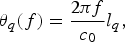 $$\theta _q \lpar f\rpar = \displaystyle{{2\pi f} \over {c_0 }}l_q\comma \;$$
where c 0 is the speed of light in vacuum.
The expression of the value of each capacitor, C q (q = 1,…, N + 1), is obtained by combining (1) and (3):
 $$C_q = \displaystyle{{Y_{sq} } \over {2\pi f_{zq} {\tan}\lpar \theta _q \lpar f_{zq} \rpar \rpar }}.$$
Then, the introduction of (5) in (3) and the use of the resulting equation with (2) give the characteristic admittance of the N first stubs as follows:
 $$y_s = X^{ - 1} y_{N + 1} .$$
y s is the vector of the characteristic admittances of the N first stubs:
 $$y_s=\lsqb Y_{s1}\comma \; Y_{s2}\comma \; \ldots\comma \; Y_{sN} \rsqb ^t .$$
X is an N-by-N square matrix. Its elements are defined by:
 $$x_{pq} = \displaystyle{{f_{0p} + f_{zq} {\tan}\lpar \theta _q \lpar f_{zq} \rpar \rpar {\tan}\lpar \theta _q \lpar f_{0p} \rpar \rpar } \over {f_{zq} {\tan}\lpar \theta _q \lpar f_{zq} \rpar \rpar - f_{0p} {\tan}\lpar \theta _q \lpar f_{0p} \rpar \rpar }}$$
with p = 1,2,…, N and q = 1,2,…, N.
The vector y N+1 is expressed as
 $$y_{N + 1} = - Y_{sN + 1} \; \lsqb x_{1\comma N + 1}\comma \; x_{2\comma N + 1}\comma \; \ldots\comma \; x_{N\comma N + 1} \rsqb ^t\comma \;$$
where the N coefficients x p,N+1 are given by (8) with q = N + 1.
In this synthesis, the physical length of the N + 1 stubs and the characteristic admittance of the last one, Y sN+1, are freedom degrees. They can be used to obtain achievable characteristic admittances and values of capacitors according to the technological constraints or to provide different values of the slope parameter even if the latter is not taken into account in the synthesis equations.
III. RECONFIGURABLE TRI-BAND RESONATOR
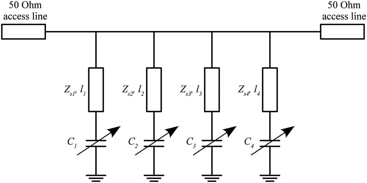
An example of a reconfigurable tri-band resonator in ideal transmission lines is presented in this section. Its development is outlined in two steps: the first one consists of obtaining the length and the impedance of the four stubs and the initial value of the four associated capacitors using the synthesis presented in the previous section; the second step presents how the variations of the values of the capacitors allow the frequency of the transmission zeros to be independently controlled and so how the three resonant frequencies can be tuned.
A) Initial configuration
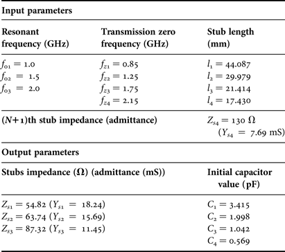
Figure 3 presents the scheme of a reconfigurable tri-band resonator in an ideal transmission lines configuration. The synthesis presented in Section II gives the admittance of the first three stubs (Y s1, Y s2 and Y s3), and so their impedance (Z s1, Z s2 and Z s3), plus the initial value of the four capacitors (C 1, C 2, C 3 and C 4). The input parameters are the three resonant frequencies (f 01, f 02 and f 03), the frequency of the four transmission zeros (f z1, f z2, f z3 and f z4), the impedance of the fourth stub (Z s4 = 1/Y s4) and the length of all stubs (l 1, l 2, l 3 and l 4). According to the technological constraints used in Section IV for demonstration, we fixed the impedance Z s4 equal to 130 Ω and the length of each stub, l i, equal to λ zi/8, where λ zi = c 0/f zi (i = 1–4). One should note that the ratio between l i and λ zi could be different from one stub to another. This choice was made to simplify the demonstration. Figure 4 shows the simulated electrical response of this resonator and Table 1 summarizes all the input and output parameters of the tri-band synthesis. This response will be referred to as the initial configuration in the next subsection.
Fig. 3. Scheme of a reconfigurable tri-band resonator in an ideal transmission lines configuration.
Fig. 4. Simulated electrical response of the synthesized tri-band resonator in its initial configuration.
Table 1. Input and output parameters of the synthesis for a reconfigurable tri-band resonator.
B) Reconfiguration of the tri-band resonator
From this initial configuration, one can change the value of the four capacitors to control the position of the four transmission zeros. Indeed, in the DBR topology, each bandstop structure (i.e. a stub and its associated capacitor here) controls the frequency of a transmission zero independently from the others. So, the variation of the value of a capacitor, C i, only impacts on the frequency of the ith transmission zero, f zi, and has no influence on the others. Figure 5 presents the evolution of the tri-band resonator electrical response when the values of the four capacitors decrease one by one from their initial value. Thus, Fig. 5(a) shows the moving of f z4 from 2.15 to 2.25 GHz when C 4 decreases from 0.569 to 0.506 pF; Fig. 5(b) the moving of f z3 from 1.75 to 1.85 GHz when C 3 decreases from 1.042 to 0.896 pF; Fig. 5(c) the moving of f z2 from 1.25 to 1.35 GHz when C 2 decreases from 1.998 to 1.638 pF and Fig. 5(d) the moving of f z1 from 0.85 to 0.95 GHz when C 1 decreases from 3.415 to 2.527 pF.
Fig. 5. Change of the simulated electrical response of the tri-band resonator depending on the variations of the capacitors. (a) Variation of C 4 from 0.569 pF (red dashed lines) to 0.506 pF (blue solid lines), C 1 = 3.415 pF, C 2 = 1.998 pF, and C 3 = 1.042 pF in both cases. (b) Variation of C 3 from 1.042 pF (red dashed lines) to 0.896 pF (blue solid lines), C 1 = 3.415 pF, C 2 = 1.998 pF, and C 4 = 0.506 pF in both cases. (c) Variation of C 2 from 1.998 pF (red dashed lines) to 1.638 pF (blue solid lines), C 1 = 3.415 pF, C 3 = 0.896 pF, and C 4 = 0.506 pF in both cases. (d) Variation of C 1 from 3.415 pF (red dashed lines) to 2.527 pF (blue solid lines), C 2 = 1.638 pF, C 3 = 0.896 pF, and C 4 = 0.506 pF in both cases.
The independence of the transmission zeros offers a lot of possibilities to reconfigure the resonator response and not only the resonant frequencies. For instance, Fig. 6 presents the removing of the second resonance, f 02, by bringing f z2 and f z3. One can also suppress another resonance; modify the three bandwidths, etc.
Fig. 6. Suppression of the central passband of the tri-band resonator by varying C 2 and C 3 from 1.998 and 1.042 pF (red dashed lines) to 1.199 and 1.511 pF (blue solid line), respectively (C 1 = 3.415 pF and C 4 = 0.569 pF in both cases).
IV. EXPERIMENTAL VALIDATION USING VARACTOR DIODES ON MICROSTRIP TECHNOLOGY
A) Prototype characteristics and measurements setup
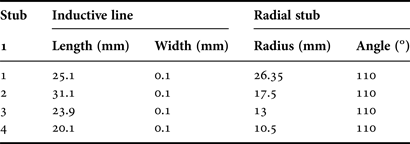
The tri-band resonator synthesized in Section III has been realized in microstrip technology on a RO4003 Rogers substrate (dielectric constant: ε r = 3.55, height: h = 0.508 mm, dissipation factor: tan δ = 0.0027) with copper metallization (metal width: t = 17.5 µm, conductivity: σ = 5.8 × 10⁷ S/m). Varactor diodes are used as variable capacitors. Table 2 summarizes the characteristics of the bandstop structures. The tri-band resonator was simulated and optimized using Agilent ADS software and especially the EM-cosimulation tools allowing an easy integration of the mounted components characteristics (diodes, capacitances) into the simulations. All varactor diodes are from the MGV125 family from Aeroflex Metelics, with a 0805-02 CMS packaging. Nevertheless, three different models are used (MGV125-20, MGV125-22, and MGV125-26) according to the required range of capacitance values. The fabricated prototype also includes DC bias circuits for the four varactor diodes. They are composed of a decoupling capacitance (10 nF) connected to the ground by a metallic via hole, an inductive line and a radial stub. Each bias circuit was designed at the initial frequency of the associated transmission zero. Their dimensions are presented in Table 3. The input and output lines width is 1.8 mm. One should note that these RF input/output lines behave as a common DC ground for all varactor diodes. DC-block (BLK-18-S+ from Mini-Circuits) is used between the SMA accesses of the circuit and the Vector Network Analyzer ports. The latter is an ENA 5062A from Agilent Technologies. Figure 7 presents a picture of the manufactured reconfigurable tri-band resonator (a) and a detailed view of a bias circuit of one of the varactor diodes (b).
Fig. 7. Picture of the manufactured reconfigurable tri-band resonator (Ruler unit: centimeter) (a) and detailed view of the bias circuit of the varactor diode associated with stub 4 (b).
Table 2. Manufactured reconfigurable tri-band resonator: optimized dimensions of the stubs and diodes used.
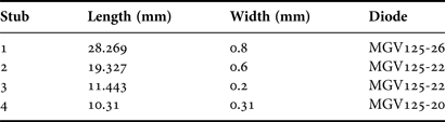
Table 3. Manufactured reconfigurable tri-band resonator: biasing circuits characteristics.
B) Measurements results
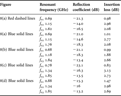
The measurements presented in Fig. 8 show the moving of the four transmission zeros due to the variations of the DC bias voltages (V i, i = 1, 2, 3, or 4; cf. Fig. 7) applied to the four diodes. In this example, each DC bias voltage, V i, increases, so the associated diode capacitor value, C i, decreases and the frequency of the transmission zero, f zi, moves up. Thus, a variation of V 4 from 5.8 to 8.2 V implies that f z4 moves from 1.97 to 2.18 GHz (cf. Fig. 8(a)); a variation of V 3 from 5.2 to 7.3 V implies that f z3 moves from 1.38 to 1.59 GHz (cf. Fig. 8(b)); a variation of V 2 from 3.1 to 5.1 V implies that f z2 moves from 0.93 to 1.20 GHz (cf. Fig. 8(c)) and a variation of V 1 from 1.5 to 4 V implies that f z1 moves from 0.47 to 0.69 GHz (cf. Fig. 8(d)).
Fig. 8. Change of the measured electrical response of the tri-band resonator depending on the bias voltages. (a) Variation of V 4 from 5.8 V (red dashed lines) to 8.2 V (blue solid lines), V 1 = 1.5 V, V 2 = 3.1 V, and V 3 = 5.2 V in both cases. (b) Variation of V 3 from 5.2 V (red dashed lines) to 7.3 V (blue solid lines), V 1 = 1.5 V, V 2 = 3.1 V, and V 4 = 8.2 V in both cases. (c) Variation of V 2 from 3.1 V (red dashed lines) to 5.1 V (blue solid lines), V 1 = 1.5 V, V 3 = 7.3 V, and V 4 = 8.2 V in both cases. (d) Variation of V 1 from 1.5 V (red dashed lines) to 4 V (blue solid lines), V 2 = 5.1 V, V 3 = 7.3 V, and V 4 = 8.2 V in both cases.
Figure 8 shows a fifth transmission zero between 2.4 and 2.6 GHz. In fact, it is the first harmonic of the first transmission zero, f z1. Thus, its frequency also varies when the DC voltage V 1 is modified. Its presence implies a fourth resonance between 2.2 and 2.4 GHz more or less stronger depending on its proximity with the fourth transmission zero, f z4.
One should also note in Fig. 8 that the increase of some bias voltages can also imply very slight decrease of the frequency of unassociated transmission zeros. For instance, in Fig. 8(a), f z2 decreases when V 4, and so f z4, increase. This is due to an insufficient isolation between each varactor diode mainly because RF input/output lines are used as DC common ground. Indeed, a small part of the bias signal of one diode goes to the other diodes and not to the ground through the DC-block as expected. It modifies slightly the bias voltage applied to the other diodes and so the frequency of the other transmission zeros. The latter move down because the undesired bias signal feeds the diodes by their anode, and not by their cathode and so subtracts from the main bias voltage. A better isolation could be obtained adding an inductance in parallel connected to the ground and a capacitance in series close to each varactor diode. This allows all the bias signals not to be mixed but this solution increases design complexity and highly decreases the resonator performance. This is a limitation of the use of diodes in such a case, the bias control signals flowing in the microwave circuit. Nevertheless, this technological default, clearly identified, does not call into question the concept proposed here. Other reconfiguration technologies could be investigated to overcome this problem.
As explained in Section III, the independence of the four transmission zeros offers a lot of possibilities to reconfigure the tri-band resonator. The tuning of the three resonant frequencies is thereby demonstrated in Fig. 8. Between the first measured configuration (Fig. 8(a) – red dashed lines) and the last one (Fig. 8(d) – blue solid lines), the variation of the four bias voltages leads to a shifting of f 01 from 0.69 to 0.88 GHz (27.5%), of f 02 from 1.15 to 1.34 GHz (16.5%), and of f 03 from 1.63 to 1.85 GHz (13.5%). Another example is given in Fig. 9. The second passband is easily suppressed by increasing V 2 (from 2.8 to 5.3 V) and decreasing V 3 (from 5.4 to 4.3 V), V 1 and V 4 remaining constant.
Fig. 9. Measured S-parameters of the realized tri-band tunable resonator with suppression of one band (red dashed lines: V 1 = 1.45 V, V 2 = 2.8 V, V 3 = 5.4 V, and V 4 = 6 V, blue solid lines: V 1 = 1.45 V, V 2 = 5.3 V, V 3 = 4.3 V, and V 4 = 6 V).
C) Measurements analysis
Experimental reflection coefficients and insertion losses at the three resonant frequencies of the five cases presented in Fig. 8 are summarized in Table 4. The first are always lower than −13 dB. It is quite satisfactory for a reconfigurable multi-band resonator allowing a frequency shift better than 13% for each resonance. Insertion losses are between 0.9 and 3 dB according to the bandwidth. They are in correlation with the insertion losses estimated by simulation. As an example, Fig. 10 presents a comparison between simulation and measurement for one of the five cases (V 1 = 1.5 V, V 2 = 3.1 V, V 3 = 5.2 V, and V 4 = 5.8 V in red dashed lines in Fig. 8(a)).
Fig. 10. Simulation (red dashed lines) and measured (blue solid lines) S-parameters of the tri-band resonator for V 1 = 1.5 V, V 2 = 3.1 V, V 3 = 5.2 V, and V 4 = 5.8 V.
Table 4. Measured reflection coefficients and insertion losses.
In simulation, a varactor diode model is used with a series resistance of 0.3 Ω. The bias circuits are also taken into account. To estimate the losses due to these elements (diodes and biasing circuits), a comparison was made in simulation between an electrical response of the reconfigurable tri-band resonator and a passive DBR tri-band resonator giving a similar response. This passive resonator was designed using [Reference Quendo, Manchec, Clavet, Rius, Favennec and Person14] and the same technological properties as the reconfigurable one (substrate, metallization). It has the same transmission zeros frequencies and slightly different resonant frequencies due to different slope parameters. Figure 11 presents these simulations results. The insertion losses are 0.25 dB for the first resonance, 0.73 dB for the second and 0.62 for the third in the passive case instead of 0.69, 1.15, and 1.62 dB, respectively in the reconfigurable case. The integration of diodes and biasing circuits leads to an increase in the insertion losses from about 0.5–1 dB according to the frequency. We estimate that the insertion of the diodes divides the values of the quality factor by approximately 2. Nevertheless, despite this well-known default of such components, we chose this solution for its simplicity and low-cost. Others reconfiguration solutions can be used to avoid these additional losses.
Fig. 11. Simulated S-parameters of the reconfigurable tri-band resonator (V 1 = 1.5 V, V 2 = 3.1 V, V 3 = 5.2 V, and V 4 = 5.8 V – red dashed lines) and a passive tri-band DBR with an equivalent response (blue solid lines).
One should note in Fig. 11 that a transmission zero, called f z1h, appears close to f z3 in the passive case. It is the first harmonic of the first transmission zero, f z1. In the passive case [Reference Quendo, Manchec, Clavet, Rius, Favennec and Person14], each bandstop structure only consists of a stub that presents a first transmission zero at f zi. The first harmonic is then located at 3f zi. In the tunable case presented here, each bandstop structure is composed of a capacitance and a stub, shorter than in the passive case to keep the same transmission zero frequency. The presence of harmonic is only due to the stub part and as it is shorter the first harmonic is higher in frequency.
V. CONCLUSION
A reconfigurable N-band resonator was presented here together with its associated synthesis. The latter allows an initial configuration of the resonator to be easily obtained. The N + 1 transmission zeros of the resulting resonator can be then independently tuned and so the electrical response of the resonator can be modified. The concept was validated through the realization of a tri-band resonator in microstrip technology and the use of varactor diodes as tuning elements.
The realization of filters implies the association of two or more reconfigurable N-band resonators. This allows more parameters (bandwidths, rejected bands, etc.) to be controlled. Nevertheless, such a realization can be very difficult particularly when the resonance frequencies are far from one to the others. So, additional investigations have to be done to integrate into the synthesis the slope parameter at each resonance and the coupling between resonators. The resulting synthesis will allow facilitating the development of reconfigurable M-order N-band filters. This would also minimize the influence of tuning on the coupling between resonators and so preserve a larger tuning frequency range.
ACKNOWLEDGEMENTS
The authors would like to thank Mr Christophe Guitton and Mr. Gilles Picoult, from the Institute of Electronics and Telecommunications of Rennes, for carrying out the printed circuit board and mounting the components respectively.
Erwan Fourn was born in Brest, France, in 1977. He received the Master degree in Electronics in 2001 and his Ph.D. degree in Electronics in 2004, both from the University of Brest. He was a Postdoctoral Fellow at the Laboratory for Analysis and Architecture of Systems (LAAS-CNRS), Toulouse, France. He is currently an Assistant Professor within the National Institute of Applied Sciences (INSA), Rennes, France. His research activities, within the Institute of Electronics and Telecommunications of Rennes (IETR), are mainly focused on the design of passive and reconfigurable reflectarray antennas and filters for microwave and millimeter wave applications.
Cédric Quendo (M'03) was born in Plouay, France, in 1974. He received the Electrical Engineer degree and the Ph.D. degree in Electrical Engineering from the University of Brest, France, in 1998 and 2001, respectively. Between 2001 and 2010, he gave courses and conducted research in several institutes and he was notably visiting researcher in 2005 at Georgia Tech, Atlanta, USA. Since 2010, he is Professor with the Electronic Department, University of Brest, France. He also conducts research with Microwaves Group of the Lab-STICC Laboratory, France. His research activities principally concern the modeling and design of microwave devices for microwave and millimeter-wave applications.
Eric Rius was born Auray in 1966. He received his Ph.D. degree in Electronics in 1994 at the University of Brest. In 1995, he was appointed assistant Professor and 10 years later Professor, always at the University of Brest. His main scientific interest is the study and design of front-end radio and especially centimetric and millimetric filters. He has published more than 130 papers, has been cited over 1100 times and has an h-index of 16. He was the TPC Chair of the European Microwave Conference (EUMC) in Paris in 2010. It was also, in 2010–2011, guest editor of the International Journal of Microwave and Wireless Technologies (Cambridge University Press, Special Issue on EuMW 2010 (IJWMT)). He obtained a CNRS delegation in 2010–2011 and during this period he performs a Visiting Professor at Nanyang Technological University NTU at Singapore for 4 months, from January to April 2011.