


Introduction
With the advancement of a mobile wireless system, the modulation scheme is becoming increasingly complex. In order to amplify the modulated signal without distorting the high PAPR (Peak-to-Average Power Ratio) waveform, the power amplifiers (PAs) are required to operate in the linear input power range. For classical amplifiers (with fixed load line and constant DC bias voltage), this implies that the overall efficiency is sacrificed because the PAs must be used under backed off conditions to assure linear operation for any instantaneous input power drive. In this respect, Doherty amplifiers and envelope tracking (ET) amplifiers, capable of modulating the load line and the dc bias voltage according to the input power level, respectively, are attracting wide attention as one of the most practical efficiency-enhancement technique to date. For further efficiency improvement, using harmonically tuned power cells have been shown to boost up the efficiency of both the Doherty [Reference Colantonio, Giannini, Giofre and Piazzon1] and ET amplifiers [Reference Mokhti, Tasker and Lees2]. However, the harmonic tuning circuits, such as those used in class-F amplifiers, could increase the size and cost of the PAs which are already complicated with the sophisticated modern architectures, unless effective measures are taken to miniaturize and simplify the circuitry. Recently, we have demonstrated extremely compact harmonic tuning stubs using composite right-/left-handed (CRLH) transmission lines (TLs) [Reference Tanaka, Koizumi and Saito3]. Despite the small size of the harmonic tuning stub, however, the DC-biasing circuits using quarter-wavelength microstrip line (MSL) stubs still took up a large area, hindering further miniaturization of the whole amplifier circuit. The conventional DC-biasing circuits also have the drawback of spurious 2nd harmonic response, thus restricting the freedom of designing harmonically tuned amplifiers.
In this paper, we present a novel DC-biasing circuit realized using a compact CRLH TL stub. We show that by engineering the dispersion diagram of the CRLH TL, the DC-biasing circuit can generate arbitrary set of transmission zeros (TZs) that can be used to realize class-F load conditions, i.e. short and open for the 2nd and 3rd harmonics, respectively. The stub can also be designed to generate reflection zeros (RZs) at the harmonic frequencies such that the stub behaves like an ideal DC-biasing circuit without spurious harmonic responses. This can simplify the difficult task of optimizing the impedance matching network with harmonic treatment while minimizing the circuit size. To verify the practicability of the proposed technique, a 2-GHz class-F GaN HEMT PA exploiting the proposed DC-biasing circuits is demonstrated.
Design and characterization of DC-biasing circuit
Basic configuration
Figure 1 illustrates the |S 21| characteristics for different configurations of the CRLH TL stub. Also shown in the figure are the dispersion diagrams for the CRLH stub lines. The uniqueness of the CRLH TL stub that we have been using lies in the use of the negative-order resonances (NORs) that occur in the left-handed (LH) region of the CRLH TL. Since the property of the electromagnetic wave in the LH region is predominantly determined by the inductors and capacitors constituting the unit cells, the TZs and the RZs due to the NORs can be arbitrarily controlled by tuning the LC elements.

Fig. 1. Schematic illustration of the |S 21| characteristics and dispersion diagram for CRLH TL stubs with (a) L-first and (b) C-first configurations.
The frequencies of the NOR are obtained, in general, by numerical calculation. However, if the length of the MSL section of the stub is zero (ℓ = 0), analytical formulas can be obtained [Reference Tanaka, Mukaida and Takata4]. For example, in the case of the C-first CRLH TL stub with two unit cells (Fig. 1(b)), the resonant frequency of m = −2 mode can be obtained as
 $$f_{-2} = 1/2\pi \sqrt {\lpar {L_1 + L_2} \rpar C_2}. $$
The analytical expressions for the m = −1 and m = −3 modes are also available but with somewhat more complicated formulations [Reference Tanaka, Mukaida and Takata4]. The formulas for the L-first CRLH TL stub with two unit cells (Fig. 1(a)) can also be derived, such as:
 $$f_{-2} = 1/2\pi \sqrt {\lpar {C_1 + C_2} \rpar L_2}. $$
Although the analytical formulas for the special case (ℓ = 0) do not apply to general cases of ℓ>0, they provide a means for roughly estimating the L and C values necessary for obtaining the TZs and RZs at the targeted frequencies.
In designing a CRLH TL stub, there are two design options: looking from the connection point of the stub, the first is to place the shunt inductor first (Fig.1(a)), and the second is to place the reactive elements the other way around (Fig.1(b)). The fundamental resonance modes of the lowest frequency provide a RZ and a TZ for the CRLH TL stubs of “L-first” and “C-first” types, respectively. Since the same applies to the short-ended and open-ended MSL stubs, it can be understood that the CRLH TL stubs of the L-first type and C-first type correspond to conventional short-ended and open-ended MSL stub, respectively.
Now, from Fig. 1(a), it can be seen that the L-first type CRLH TL stub can potentially be used as a DC-biasing circuit by feeding the DC bias via the shunt inductor nearest to the main signal line. Figure 2 shows a typical use case of the proposed CRLH TL stub as a drain DC-biasing circuit for a class-F amplifier. As shown in Fig. 1(a), the RZ of the lowest frequency produced by the L-first CRLH TL stub serves as the passband for the fundamental frequency of the amplifier, as in the case of conventional DC-biasing circuit. Since the inductor line for L 1 is not just a DC feed path but a critical element determining the RF characteristics of the stub, a shunt capacitor is used to define the length of the inductor line RF-wise.

Fig. 2. Basic configuration of the class-F amplifier using the proposed DC-biasing circuit.
Circuit design method
Dispersion diagram
The characteristics of TL stubs are determined by the phase of the stub lines. Thus, the dispersion diagram (the relationship between the phase and frequency of the TL) provides an effective tool for analyzing the behavior of the TL stubs. However, dispersion diagrams for TLs are normally defined for TLs as two-port circuits. Let us consider the case for a lossless MSL with characteristic impedance (Z 0) of 50 Ω. In this case, the MSL is perfectly matched to 50-Ω load and the dispersion diagram can be conveniently obtained by calculating the phase of the two-port S-parameter [Reference Tanaka, Mukaida and Takata4]
 $$S_{21}\, = \,e^{-j\theta _{2P}\lpar f \rpar }.$$
The dispersion diagram obtained this way, however, generally fails to predict the characteristics of a stub using the same MSL if, for example, Z 0 is non-identical with 50 Ω. Thus, a different definition of dispersion diagram is required for TLs as stub lines.
To cope with this problem, in [Reference Tanaka, Mukaida and Takata4] we introduced a dispersion diagram defined for a one-port TL:
 $$S_{33}\, = \,e^{-j2\theta _{1P}(\,f)},$$
where port 3 is defined as the connection point of the stub. Figure 3 shows the calculated dispersion diagram based on (4), i.e. θ 1P(f), for a short-ended lossless MSL stub measuring quarter-wavelength at 1 GHz. Also shown is the calculated |S 21| characteristics of the stub using the same MSL. (It is reminded that the |S 21| here has no relevance to (3).) It can be seen that θ 1P(f) is a linear function of the frequency if Z 0 = 50 Ω. In this case, θ 1P(f) is identical with θ 2P(f) which is commonly used for a two-port MSL with the same Z 0 and length. If Z 0 is non-identical with 50 Ω, however, the curvature of θ 1P(f) becomes non-linear. For example, in the case of high impedance stub line (Z 0 > 50 Ω), the slope of θ 1P(f) is increased at around the frequencies for RZs at 1 and 3 GHz, increasing the bandwidth of the |S 21| characteristics of the stub there. The commonly used DC-biasing circuits based on short-ended quarter-wave stubs thus normally use high characteristic impedance line to increase the bandwidth of the passband for the fundamental RF signal. Similarly, the bandwidth of the |S 21|(f) of the stub around the TZs can be increased by using low impedance MSLs (Z 0 < 50 Ω). Hereafter, we use the dispersion diagram based on (4) as a tool for designing the CRLH TL stubs.

Fig. 3. |S 21| characteristics of short-ended MSL stub and corresponding dispersion diagrams for one-port stub lines.
Design criteria
In general, a CRLH TL to be used as a two-port TL must be designed such that the impedance matching conditions are met for bilateral transmission of the RF signal. To meet the requirements, the CRLH TL is normally configured to have a uniform structure (using identical unit cells) with the balanced and symmetric design. Furthermore, impedance matching is taken into account by adequately choosing the Bloch impedance of the CRLH TL [Reference Caloz and Itoh5]. When designing such CRLH TLs, some key equations for balanced design conditions or Bloch impedance serves as the design criteria and help setting the values for the reactive components of the CRLH TL.
On the other hand, when dealing with a one-port CRLH TL as a stub line, it is not the characteristic impedance (or Bloch impedance) or the uniformity of the TL but the phase that matters. This can be analogically understood by the fact that MSL stubs with non-50-Ω characteristic impedance or stepped impedance [Reference Chu and Tian6] are commonly used. Thus, the values for the reactive components of CRLH TL can be varied almost arbitrarily to obtain the desired frequency response of the stub. The CRLH TL can even be non-uniform (using non-identical unit cells), because in the first place periodicity is not a necessity in the CRLH TL theory as long as the homogeneity conditions of the unit cells are met (p.100 in [Reference Caloz and Itoh5]).
Hence, it follows that there are no specific equations serving as design criteria for CRLH TL stubs. As we will see soon, the circuit designer can control the frequency response and even the physical size of the stub by tuning the curvature of the dispersion diagram. Note, however, it is not necessary to do the cumbersome task of computing the dispersion diagram every time the circuit parameters are updated during the optimization process. Instead, practically it just suffices to monitor the |S 21| frequency response of the stub while tuning the parameters, because the approximate form of the dispersion diagram θ 1P(f) can be imagined by plotting the phase versus the frequencies of the TZs and RZs which occur alternately with 90° phase interval (see Fig. 1). Although the design method is based on a trial-and-error approach, it is not a burdensome work, unless the initial parameter values are too apart from the solution. In this sense, equations such as (1) and (2) may help setting the initial values.
Circuit size control
The physical dimension of the proposed DC-biasing circuit, consisting of lumped elements and a MSL, is dominated by the length of the MSL section. Thus, to shrink the total size of the DC-biasing circuits, reducing the MSL length is more effective than using less number of unit cells.
Figure 4 shows schematic illustrations of the dispersion diagrams for the CRLH TL stub with two and three unit-cells. The frequencies are in the unit of the fundamental frequency (f 0) of the amplifier. If the number of unit-cells is saved to two, we need to use the zeroth order resonance (ZOR) mode (m = 0) for treating the 3rd harmonic, because only a single TZ (corresponding to NOR mode of m = −2) is available in the LH region. This design approach, however, inevitably reduces the gradient of the dispersion curve in the right-handed (RH) region. Since the gradient of the dispersion in the RH region is inversely proportional to the length of the MSL section of the CRLH TL stub, this results in increased size of the whole stub line [Reference Tanaka, Saito, Oka and Shibosawa7]. For example, in our preliminary design, the MSL section for the case of two unit-cell design measured as long as 16.2 mm which is comparable to the quarter-wavelength of 22.4 mm at 2-GHz.

Fig. 4. Schematic illustration of |S 21| characteristics and dispersion diagrams for the CRLH TL stubs using two and three unit cells.
Now, if we chose to use three unit-cells, five NOR modes including two modes providing TZs (m = −2, −4) are available in the LH region. As a result, it becomes possible to let the two NOR modes take care of the 2nd and 3rd harmonics while exploiting the ZOR mode for controlling the dispersion gradient in the RH region. As can be seen from Fig. 4, the ZOR mode (yielding TZ) is tuned to very high-frequency range while fixing the frequency for the two NOR modes (m = −2, −4) at the 2nd and 3rd harmonics. This is equivalent to increasing the dispersion gradient and thus to shrink the MSL section of the stub. By using three unit-cell design, the length of the MSL section was reduced from 16.2 mm to 2.5 mm. This is clearly showing the advantage of the CRLH TL stubs designed using the NOR modes, namely, the frequency characteristics and the size can be controlled independently by maneuvering the dispersion diagram in the LH and RH region, respectively.
Bandwidth control
In order for the PA to operate with high power efficiency over a certain frequency range, the frequency variation of the load impedance must be minimized not only at the fundamental frequency band but also at the harmonic frequency bands. As discussed in the previous section, the local gradient of the dispersion diagram directly affects the local bandwidth of the stub frequency characteristics. Thus, the curvature of the dispersion diagram needs to be adequately modified to meet the bandwidth requirements.
Figure 5 compares two dispersion diagrams for CRLH TL stubs with different designs (A and B) for f 0 of 2 GHz. The diagrams were calculated using Keysight ADS circuit simulator based on ideal lumped elements and TLs. Table 1 lists the parameter values used for the two types of design. It can be seen that the dispersion diagram for Design A is optimized for increased bandwidth at around f 0, whereas in Design B more emphasis is placed on increasing the bandwidth at around 2f 0 and 3f 0. Also shown in Fig. 5 is the |S 21| characteristics for the CRLH TL stubs. It can be seen that comparing the two designs, the bandwidths around the harmonic frequencies are increased for the stub based on Design B.

Fig. 5. Calculated dispersion diagrams and |S 21| characteristics for CRLH TL stubs with different designs.
Table 1. Design parameter list for CRLH transmission line stubs

Experimental results
To confirm the validity of the proposed DC-biasing circuit, two stand-alone CRLH TL stubs with different designs were fabricated and tested. The layout of the CRLH TL stub, initially designed using ADS circuit simulator, was optimized using Momentum EM simulator.
Figure 6 shows the pictures of the DC-biasing circuits fabricated on Panasonic R-5775 substrate (h = 0.63 mm, ε r = 3.6, tan δ = 0.002). The circuit serving both as a DC-biasing circuit and harmonic tuning circuit can be seen to be very compact, considering that the lengths for the conventional MSL stubs for DC biasing and 2f 0/3f 0 harmonics tuning are λ/4, λ/8, and λ/12, respectively (λ/4 equals 22.4 mm at 2 GHz under the same conditions). As for the lumped elements for the CRLH TL stub, 1005-size multilayer ceramic capacitors and short-ended MSLs were used for capacitors and inductors, respectively. Care was taken to keep the capacitance values to <1.5 pF so that the self-resonance frequency of the capacitors is sufficiently higher than the 3rd harmonic frequency. Even so, for accurate design, the non-ideal behaviors of the chip capacitors were taken into account in the simulation by using the capacitor models provided by the manufacturer. It can be seen that no capacitor is actually used for C 3 in the circuit of Design A. This is because this design required only a minimum capacitance value of around 0.1 pF for C 3 (Table 1), so a fringing capacitor at the end of the MSL could reasonably be used as a substitute of C 3.

Fig. 6. Photograph of the fabricated DC-biasing circuits of (a) Design A and (b) Design B.
Figure 7 shows the measured |S 21| characteristics of the fabricated circuits. During the measurements, the circuits were connected to the DC source via the DC bias pads. It can be seen that both types of CRLH TL stubs generate a RZ at f 0 and TZs at 2f 0 and 3f 0. Good agreement between the measurement and EM simulation was obtained at least up to around 8 GHz. Comparing the characteristics of the two designs, it can be seen that there is a tradeoff between the bandwidth at f 0 and the bandwidth at 2f 0 and 3f 0. In the next section, we will discuss how the different designs affect the amplifier performance.

Fig. 7. |S 21| characteristics of the DC-biasing circuits.
Application to class-f PA
Amplifier design
A 2-GHz class-F PA using the proposed DC-biasing circuits was designed. For simulation, a non-linear model for GaN HEMT device (CGH40006P) from Cree Inc. was used. Figure 8 shows the configuration of the class-F PA. Once the design of the proposed DC-biasing circuit was finalized, the load impedances for 2f 0 and 3f 0 are determined by the harmonic tuning section of the output matching network (OMN). So, unlike the usual load-pull analysis, we obtained the optimum f 0 load impedance for the FET including the harmonic tuning section of the OMN, as shown in Fig. 2. This method turned out to improve the convergence time of the load-pull simulation as well as the uniqueness of the solution.

Fig. 8. Configuration of class-F PA using the proposed DC-biasing circuits.
The optimum source impedance (Z S,opt) for 2 and 4 GHz thus obtained were 1.0 + j2.9 Ω and −j23.1 Ω, respectively, at the bias conditions of V gs = −3.0 V and V ds = 28 V. Meanwhile, the optimum load impedance Z L,opt was 18.6 − j17.2 Ω at 2 GHz, which led to a simple f 0 impedance matching circuit consisting of a single stub. Conventional harmonic tuning circuits using MSL stubs for class-F amplifiers affect the f 0 load impedance [Reference Tanaka, Saito, Oka and Shibosawa7], which occasionally results in difficult conditions for matching the impedance at f 0. In this respect, the CRLH TL harmonic tuning stub designed to yield RZ at f 0 has no influence on the f 0 impedance, which is another merit of using CRLH TL stub as a harmonic tuning stub.
As for the input matching network (IMN), various configurations were compared in terms of the circuit size. If the harmonic were to be terminated in short prior to f 0 impedance matching, as usual, the footprint of the IMN became large because significantly long TL was required by the above-mentioned optimum 2f 0 source impedance. We finally found that the most space-efficient solution is an IMN shown in Fig. 8. Namely, starting from the gate terminal of the FET, we firstly placed the pre-matching stubs for f 0, followed by CRLH TL stub for DC-biasing, 2f 0 tuning stub and a series capacitor for finalizing the f 0 impedance matching.
Figure 9 shows the simulated |S 21| characteristics for the CRLH TL stub designed for gate biasing. The configuration of the CRLH TL stub is shown in Fig. 8. Only two unit cells were used for this particular biasing circuit because only the 2nd harmonic impedance was to be controlled. Based on a similar design method as in the case at the drain side, two RZs and a TZ of NOR modes are placed at f 0, 2f 0, and at some frequency point in between f 0 and 2f 0, respectively. As a result, unlike the conventional DC-biasing circuit using λ/4 stub, the present circuit does not have a harmonic spurious response at 2f 0. Instead, it provides passbands at f 0 and 2f 0, and thus can be placed before the 2f 0 tuning stub without disturbing the harmonic impedance. The present CRLH TL stub for gate biasing is not intended for providing harmonic short (TZ) at 2f 0. Hence, it was designed based on an approach similar to the case of the drain biasing circuit of Design A (wider bandwidth for the passband).

Fig. 9. Simulated |S 21| characteristics of the gate DC-biasing circuit.
Measurement results
Figure 10 shows the photograph of the fabricated PA. Compared with the MSL quarter-wavelength of 22.4 mm at 2 GHz, the CRLH TL stub can be seen to be compact in size taking up only small area of the whole circuit. Unconditional stability of the amplifier was assured by using series and shunt resistors in the IMN.
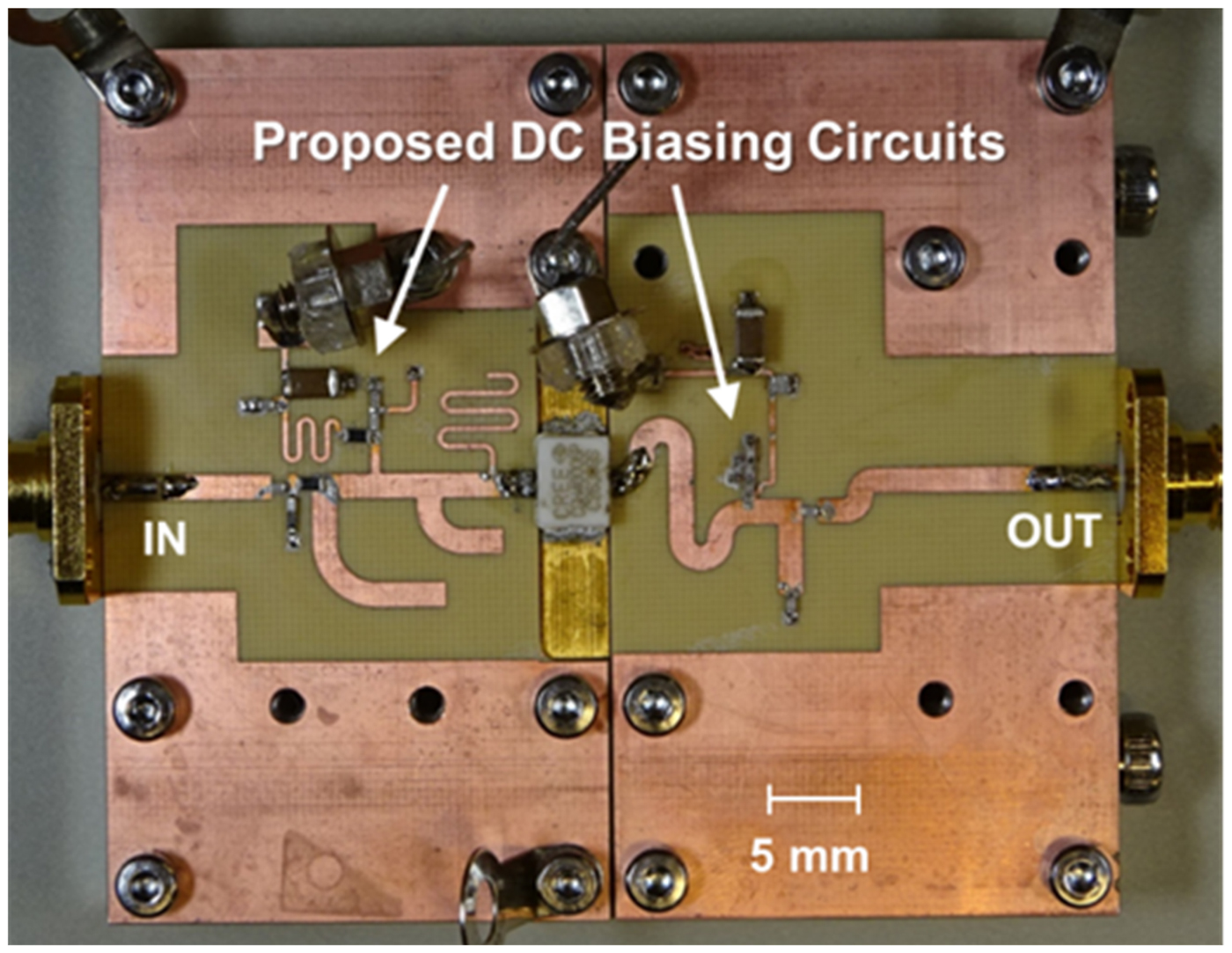
Fig. 10. Photograph of the fabricated 2-GHz PA.
Figure 11 plots the measured power performance of the amplifier at the biasing conditions of V gs = −3.0 V and V ds = 28 V. The maximum power-added efficiency (PAE) was 77.3% when the drain efficiency (DE) and the output power were 85.8% and 38.6 dBm, respectively.
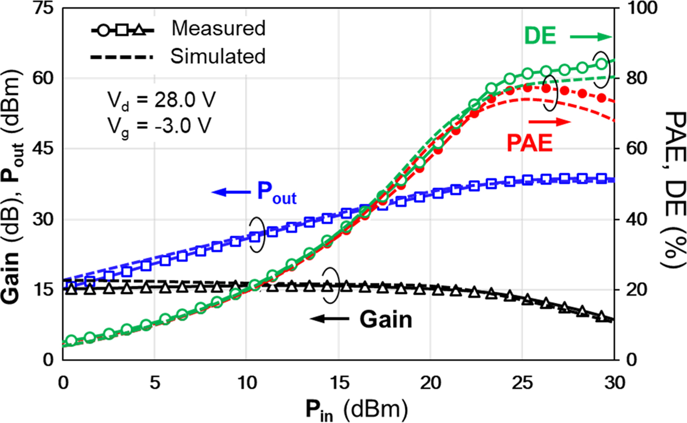
Fig. 11. Power performance of the fabricated 2-GHz PA.
Figure 12 shows the output spectrum of the amplifier measured at the input drive conditions of 3-dB backed off from saturation. It can be seen that the 2nd and 3rd harmonics are suppressed with regard to the fundamental frequency by −48.8 and −51.5 dB, respectively, whereas the suppression for the 4th harmonic (not treated in the present PA design) is −33.0 dB. The results are an indirect indication of the successful class-F harmonic operation of the amplifier using the proposed DC-biasing circuits.

Fig. 12. Output spectrum of the fabricated 2-GHz PA.
Discussion
Modern mobile communication system requires high-efficiency operation of the PAs over a wide frequency range. Figure 13 compares the frequency dependence of the maximum PAE for two PAs using drain biasing circuits based on “Design A” and “Design B”. As can be seen, the simulation predicts that the PA with “Design B” maintains high PAE (>65%) over wider bandwidth than the PA with “Design A”. The measured results for the PA based on Design B shows a similar frequency dependence of maximum PAE. The sharp decrease in PAE at 2.11 GHz results from the 2nd harmonic source impedance approaching the worst impedance conditions point which tends to be located close to the 2nd harmonic optimum source impedance [Reference Enomoto, Ishikawa and Honjo8].

Fig. 13. Frequency dependence of the maximum PAE for PAs with different designs.
Table 2 summarizes the power performance of S-band GaN FET PAs with moderate output power (<12 W) [Reference Yao, Ishikawa and Honjo9–Reference Chen and Peroulis12]. The power efficiencies achieved with the present compact PA compares favorably well with those of the state-of-the-art PAs.
Table 2. Comparison of S-band GaN FET PAs with output power of <12W

Finally, although the present work only addressed the effect of the proposed DC-biasing circuit on the efficiency, the technique could also be useful for improving the linearity with a compact circuit size. For example, studies have shown that the 2nd harmonic tuning at the gate side improves the linearity of the PAs [Reference Watanabe, Takatsuka, Takagi, Kuroda and Oda13]. Thus, the CRLH-TL-based DC-biasing circuits with controlled harmonic responses are expected to increase the circuit design freedom for improving the linearity as well.
Conclusion
Novel DC-biasing circuits based on CRLH TL and their applications to compact harmonically tuned PAs were presented. The proposed circuits take advantage of the strongly nonlinear dispersion diagram of the CRLH TL stub, which becomes possible by using the NORs in the LH region. Two design examples for the versatile DC-biasing circuit were presented. One is the DC-biasing circuit that can also be used as harmonic tuning circuit for class-F amplifier and the other is the one that almost appears to be an ideal DC-biasing circuit without spurious harmonic responses. Taking advantage of the unique properties of the CRLH TL stub based on the NORs, the proposed DC-biasing circuit should be able to be tuned for even wider applications. The class-F PA fabricated in this work showed promising results for applications to more advanced PAs requiring high circuit integration level with minimum circuit size.
Acknowledgements
The authors would like to thank Prof. Kazuhiko Honjo for helpful advice.
 Shinichi Tanaka received the B.E. and M.E. degrees in applied physics from the University of Tokyo and the D.E degree in Electrical Engineering from Tohoku University in 1984, 1986, and 1997, respectively. In 1986, he joined Central Research Laboratories, NEC Corporation, where he was involved in the development of GaAs and InP HBTs and their applications to microwave and millimeter-wave MMICs. From 1992 to 1993, he was at Purdue University, IN, USA, as a Visiting Scholar. From 2005 to 2009, he was a Visiting Professor at the University of Electro-Communication. Since 2009, he has been a Professor at the Department of Information and Communications Engineering, Shibaura Institute of Technology, Tokyo. His current research interests include microwave power amplifiers, low phase-noise oscillators, and rectifiers for microwave power transmission. Dr. Tanaka is a senior member of the IEEE, IEICE, and IEEJ.
 Tomoya Oda received the B.E. degree in Communications Engineering in 2017 and the M.E. degree in Electrical Engineering and Computer Science in 2019, both from Shibaura Institute of Technology. Mr. Oda is a member of the IEICE. Since 2019, he is with Murata Manufacturing Co., Ltd.
 Kento Saiki received the B.E. degree in Electrical Engineering in 2017 and the M.E. degrees in Electrical Engineering and Computer Science in 2019, both from Shibaura Institute of Technology. Mr. Saiki is a member of the IEICE. Since 2019, he is with Mitsubishi Electric Corporation.


