


I. INTRODUCTION
Reflectarray antennas have been introduced as an alternative to the conventional reflector antennas [Reference Huang and Encinar1]. The microstrip reflectarrays are low-cost and light weight. These antennas can replace commonly used reflectors in many applications. Reflectarray antennas are quasi-periodic structures with the capability of shifting the phase of the incident wave. The amount of phase shift can be adjusted in each cell such that the reflected wave attains a desired wave front. Thus, each cell should have the capability of local phase shifting in a wide range of values. The phase diagram of a reflectarray antenna may be obtained by changing one or several features of its unit cell, e.g. phase delay lines [Reference Malfajani and Atlasbaf2–Reference Malfajani and Atlasbaf4], size [Reference Hamzavi-Zarghani and Atlasbaf5], effective permittivity [Reference Moeini-Fard and Khalaj-Amirhosseini6], etc. In addition, the realization of a reflectarray using metallic grating embedded in periodic anisotropic grounded slab has been studied by the authors in [Reference Rafaei-Booket and Atlasbaf7]. Controlling the phase response of the unit cell can be also obtained by mounting an artificial anisotropic superstrate on an artificial magnetic conductor (AMC) structure. Note that AMC, known as perfect magnetic conductor (PMC), forces the tangential magnetic field to zero on its boundary [Reference Balanis8]. In addition, artificial anisotropic dielectrics are inhomogeneous media that can be composed of periodic structures with two alternating different isotropic dielectrics [Reference Collin9, Reference Grann, Moharam and Pommet10]. Such periodic structures can be utilized to realize low loss media exhibiting significant anisotropy, especially at microwave or millimeter wave frequencies. To realize a three-dimensional (3D) artificial anisotropic dielectric, we use a low loss dielectric in which a bi-periodic array of air cavities is drilled. In [Reference Moeini-Fard and Khalaj-Amirhosseini6], the inhomogeneous dielectric layer on a perfect electric conductor (PEC) ground plane has been presented as a reflectarray antenna. However, it has several shortcomings such as complicated mechanical process and thick dielectric layer to provide the required phase shift with variable electrical permittivity at each cell of reflectarray. Here, we have used an inhomogeneous dielectric layer on a PMC plane as a new approach to reduce the mentioned shortcomings. To this end, periodic holes are drilled in the superstrate slab mounted on an AMC structure. By filling these holes with other material, the dielectric characteristics of the proposed unit cell are periodically varied as for example in photonic band gap (PBG) materials. Therefore, this allows controlling the dielectric properties and the phase response of the unit cell. In addition, the drilled cavity inside a cell with periodic boundary conditions is itself a resonating structure. Hence, it can increase the number of resonance frequencies. To the best of our knowledge, the proposed reflectarray antenna was never reported in the literature. In order to design a reflectarray antenna, extraction the phase response of the diffracted reflected wave is required. As the first step to accurately compute the phase diagram of the introduced unit cell, an efficient technique is required to analyze it.
In this paper, the proposed unit-cell, similar to any other planar periodic structures such as frequency selective surfaces (FSSs), is analyzed by means of the method of moments (MoM) [Reference Mittra, Chan and Cwik11]. Since the diffraction orders are coupled within inhomogeneous periodic superstrate used in this work, the dyadic Green's function is no longer diagonal for such a medium. Therefore, an efficient full-vector technique based on an equivalent transmission line (TL) formulation of Maxwell's equation [Reference Shahabadi, Atakaramians and Hojjat12] is exploited to obtain the dyadic Green's function used in the integral equation. As a result, the computed phase diagram within the usable bandwidth of AMC structure (13.95–14.95 GHz) is employed in the design of a new reflectarray antenna which is applicable for the satellite services. In this antenna, the size of patches remains unchanged and the required phase shifts in AMC bandwidth are obtained by varying the radius of air holes. The resulting reflectarray is linearly polarized and operates in Ku-band with a center-feed configuration. In addition, the total thickness of the antenna is only 0.127 cm.
II. DEFINATION AND FORMULATION OF THE PROBLEM
The aim of this section is to develop a computational technique for the analysis of the plane wave diffraction by an artificial anisotropic dielectric supported by an AMC structure.
The simplified schematic of the studied periodic structure and its unit cell are shown in Fig. 1. For the analysis, we use the technique of the spectral dyadic Green's function which is utilized in an integral equation formulation for computing the induced surface electric currents on the metallic grating. As far, the dielectric layers used in the proposed structure are homogeneous and isotropic; one can evaluate the dyadic Green's function by using the spectral immitance approach as described in [Reference Itoh13]. Afterwards, the obtained integral equation can be solved by means of MoM, which gives the induced surface electric current densities and thereby the scattered fields. In the artificial anisotropic superstrate which is investigated in this work, the diffraction orders are coupled inside such a region. Therefore, to derive an accurate dyadic Green's function, a full-vector method must be used. To do so, we use a fully vectorial rigorous matrix method based on an equivalent TL modeling in the spectral domain. This method, which will be explained in the following subsection, uses matrix formulation which simplifies the mathematics involved in the modeling of the mentioned coupling within an artificial anisotropic medium. Note that the proposed method does not use the effective medium theory (EMT) [Reference Rytov14] for the analysis.

Fig. 1. (a) Geometry of the periodic structure and (b) simplified sketch of the proposed unit cell.
A) Equivalent TL modeling
In order to derive a required equivalent TL model, it is assumed that the plane wave is incident on the proposed structure of Fig. 1(a). The electric field of the plane wave is given by
 $${{\bf E}^{inc}} = {{\bf E}_0}{{\rm e}^{{\rm (} - j{k_0}(\sin \theta \cos \varphi \hat{x} + \sin \theta \sin \varphi \hat{y} + \cos \theta \hat{z})\cdot {\bf r}{\rm )}}},$$
where k
0 is the incident wave number in free space and
 ${\bf r} = x\hat x + y\hat y + z\hat z$
is the position vector. Thus, the sum of the incident and reflected fields satisfies
${\bf r} = x\hat x + y\hat y + z\hat z$
is the position vector. Thus, the sum of the incident and reflected fields satisfies
 $${\bf E}({\bf r + L}){\bf = E}({\bf r})\exp ( - j{\bf k}\!\cdot \!{\bf L}{\rm ),}$$
 $${\bf H}({\bf r + L}){\bf = H}({\bf r}){\rm exp(} - j{\bf k}\!\cdot\! {\bf L}{\rm ),}$$
where
 ${\bf L} = {L_x}\hat x + {L_y}\hat y$
in which L
x
and L
y
are the dimensions of a unit cell in the x- and y-directions as shown in Fig. 1(b), respectively, and the vector
${\bf L} = {L_x}\hat x + {L_y}\hat y$
in which L
x
and L
y
are the dimensions of a unit cell in the x- and y-directions as shown in Fig. 1(b), respectively, and the vector
 ${\bf k} = {k_x}\hat x + {k_y}\hat y$
with
${\bf k} = {k_x}\hat x + {k_y}\hat y$
with
 ${k_x} = {k_0}\sin \theta \cos \varphi $
and
${k_x} = {k_0}\sin \theta \cos \varphi $
and
 ${k_y} = {k_0}\sin \theta \sin \varphi $
denotes the x- and y-components of the incident wave vector in which (θ, φ) are the angles characterizing the direction of the incident plane wave. The periodicity of the structure requires the electric and magnetic fields to be represented by the following pseudo-Fourier series [Reference Shahabadi, Atakaramians and Hojjat12]:
${k_y} = {k_0}\sin \theta \sin \varphi $
denotes the x- and y-components of the incident wave vector in which (θ, φ) are the angles characterizing the direction of the incident plane wave. The periodicity of the structure requires the electric and magnetic fields to be represented by the following pseudo-Fourier series [Reference Shahabadi, Atakaramians and Hojjat12]:
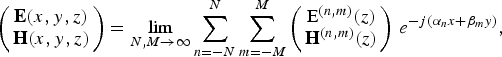 $$\left( {\matrix{ {{\bf E}(x,y,z)} \cr {{\bf H}(x,y,z)} \cr } } \right) = \mathop {\lim }\limits_{N,M \to \infty } \sum\limits_{n = - N}^N {\sum\limits_{m = - M}^M {\left( {\matrix{ {{{\bf {\rm E}}^{(n,m)}}(z)} \cr {{{\bf H}^{(n,m)}}(z)} \cr } } \right)\,{e^{ - j({\alpha _n}x + {\beta _m}y)}}} }, $$
where α n = 2πn/L x + k x and β m = 2πm/L y + k y are x- and y-wave numbers of the Floquet mode (n, m), respectively. In (4), E (n,m)(z) and H (n,m)(z) are unknown coefficients to be determined. Using these coefficients, we introduce a matrix representation for the fields and reformulate the Maxwell's equations in a matrix form. we define a K × 1 matrix [E x (z)] whose K = (2N + 1) × (2M + 1) entries are the x-component of E (n,m)(z), where the index n and m run over the integer values from −N to N and −M to M, respectively. Similarly, one can define the column matrices [E y (z)], [E z (z)], [H x (z)], [H y (z)], and [H z (z)]. To derive an equivalent TL model for our problem, we should first divide the proposed structure into parallel z-invariant layers as shown in Fig. 2.

Fig. 2. Subdividing the structure into parallel z-invariant layers required for equivalent TL modeling.
As it can be seen in the figure, the first layer is the transmission region, the second layer is the substrate of AMC structure and the last layer is the incidence region. These layers are homogeneous and isotropic. The third layer is the grating region with periodicity L
x
in the x-direction and L
y
in the y-direction and made of alternate isotropic dielectrics with relative permittivity ε
d
and ε
c
. It is assumed that all layers are non-magnetic with μ
r
= 1. Note that the relative permittivity of the third layer is a periodic function of x and y with periods of L
x
and L
y
. Hence, the relative permittivity of the ith layer (i = 1, 2, 3, 4) can be expressed as a matrix by expanding it in a Fourier series whose entries are
 $\tilde{\varepsilon} _i^{(n,m)} $
, i.e.
$\tilde{\varepsilon} _i^{(n,m)} $
, i.e.
 $${\varepsilon _{ri}}({\bf r}) = \mathop {\lim} \limits_{N,M \to \infty} \sum\limits_{n = - N}^N {\sum\limits_{m = - M}^M {\tilde \varepsilon _i^{(n,m)} (z){e^{ - j((2n\pi /{L_x})x + (2m\pi /{L_y})y)}}}}. $$
The coefficients
 $\tilde \varepsilon _i^{(n,m)} (z)$
in the homogeneous and isotropic layers (i = 1, 2, or 4) are reduced to
$\tilde \varepsilon _i^{(n,m)} (z)$
in the homogeneous and isotropic layers (i = 1, 2, or 4) are reduced to
 $\tilde \varepsilon _{ri}^{(n,m)} {\delta _{nm}}$
in which δ
nm
denotes the Kronecker delta. For artificial anisotropic layer (i = 3), the coefficients
$\tilde \varepsilon _{ri}^{(n,m)} {\delta _{nm}}$
in which δ
nm
denotes the Kronecker delta. For artificial anisotropic layer (i = 3), the coefficients
 $\tilde \varepsilon _3^{(n,m)} (z)$
are given by
$\tilde \varepsilon _3^{(n,m)} (z)$
are given by
 $$\tilde \varepsilon _3^{(n,m)} (z) = \displaystyle{1 \over {{L_x}{L_y}}}\int_0^{{L_x}} {\int_0^{{L_y}} {{\varepsilon _{r3}}({\bf r})\,}} {e^{j((2n\pi /{L_x})x + (2m\pi /{L_y})y)}}dxdy,$$
which can be evaluated either analytically or numerically. In general, for a biaxial artificial anisotropic dielectric, suppose that the cross section shape of periodic holes in Fig. 1 is elliptical where (a, b) are their principal axes. Also assume that such a hole is drilled in the center of a unit cell in the third layer. Thus, for |x| ≤ L x /2 and |y| ≤ L y /2
 $${\varepsilon _{r3}}({\bf r}) = \left\{ {\matrix{{{\varepsilon _c}} & {{{\left( {\displaystyle{x \over {a/2}}} \right)}^2} + {{\left( {\displaystyle{y \over {b/2}}} \right)}^2} \le 1} \cr {{\varepsilon _d}} & {{\rm otherwise}} \cr } } \right. $$
By substituting (7) into (6), one can obtain
 $$\eqalign{\tilde \varepsilon _3^{(n,m)} (z) & = {\varepsilon _d}{\delta _{nm}} + 2\pi ({\varepsilon _c} - {\varepsilon _d}) \cr & \quad \displaystyle{a \over {2{L_x}}}\displaystyle{b \over {2{L_y}}}Jinc\left( {2\pi \sqrt {{{\left( {\displaystyle{{na} \over {2{L_x}}}} \right)}^2} + {{\left( {\displaystyle{{mb} \over {2{L_y}}}} \right)}^2}}} \right),} $$
where Jinc(x) = J
1(x)/x in which J
1 is the Bessel function of the first kind and first order. Once the expansion coefficients
 $\tilde \varepsilon _i^{(n,m)} (z)$
are determined for layer i, the constitutive relations (
$\tilde \varepsilon _i^{(n,m)} (z)$
are determined for layer i, the constitutive relations (
 ${\bf D}({\bf r}) = {\varepsilon _0}{\varepsilon _{ri}}({\bf r}){\bf E}({\bf r})$
and
${\bf D}({\bf r}) = {\varepsilon _0}{\varepsilon _{ri}}({\bf r}){\bf E}({\bf r})$
and
 ${\bf B}({\bf r}) = {\mu _0}{\bf H}({\bf r})$
) in each layer can be converted to equivalent matrix equations according to [Reference Shahabadi, Atakaramians and Hojjat12]. Then, in each layer, the proposed solution given by (4) along with the obtained equivalent matrix equations of the constitutive relations, will be substituted in Maxwell's equations. Now, we assume ([E
x
], [E
y
])T and ([H
y
], −[H
x
])T as the line voltages ([V(z)]) and currents ([I(z)]), respectively. After some algebraic manipulations, a set of coupled-wave equations are obtained as follows:
${\bf B}({\bf r}) = {\mu _0}{\bf H}({\bf r})$
) in each layer can be converted to equivalent matrix equations according to [Reference Shahabadi, Atakaramians and Hojjat12]. Then, in each layer, the proposed solution given by (4) along with the obtained equivalent matrix equations of the constitutive relations, will be substituted in Maxwell's equations. Now, we assume ([E
x
], [E
y
])T and ([H
y
], −[H
x
])T as the line voltages ([V(z)]) and currents ([I(z)]), respectively. After some algebraic manipulations, a set of coupled-wave equations are obtained as follows:
 $$\displaystyle{d \over {dz}}\left( {\matrix{ {[V(z)]} \cr {[I(z)]} \cr}} \right) = - j\omega \left( {\matrix{ 0 & {[L]} \cr {[C]} & 0 \cr}} \right)\left( {\matrix{ {[V(z)]} \cr {[I(z)]} \cr}} \right),$$
in which the matrices [L] and [C] are the 2K × 2K dimensions, and are determined according to [Reference Shahabadi, Atakaramians and Hojjat12]. This equation governs the electromagnetic fields propagating inside artificial anisotropic and other isotropic layers shown in Fig. 2. In equation (9), the matrices [L] and [C] are the inductance and capacitance per length matrices of the equivalent TL model corresponded to each layer. To decouple and normalize the TLs in each layer, one can use the following transformation:
 $$[{V^{(i)}}(z)] = [{P^{(i)}}][{\tilde{V}^{(i)}}(z)],$$
 $$[{I^{(i)}}(z)] = [{Q^{(i)}}][{\tilde{I}^{(i)}}(z)],$$
where 2K × 2K matrices [P
(i)] and [Q
(i)] are constant matrices which are given by the eigenvectors of ω2
[L
(i)][C
(i)] and ω2
[C
(i)] [L
(i)], respectively. To satisfy equation (9), the elements of the unknown vectors
 $[{\tilde{V}^{(i)}}(z)] = {( \ldots, \tilde{V}_n^{(i)} (z),\tilde{V}_{n + 1}^{(i)} (z), \ldots )^T}$
and
$[{\tilde{V}^{(i)}}(z)] = {( \ldots, \tilde{V}_n^{(i)} (z),\tilde{V}_{n + 1}^{(i)} (z), \ldots )^T}$
and
 $[{\tilde{I}^{(i)}}(z)] = {( \ldots, \tilde{I}_n^{(i)} (z),\tilde{I}_{n + 1}^{(i)} (z), \ldots )^T}$
in (10) and (11) are determined to be
$[{\tilde{I}^{(i)}}(z)] = {( \ldots, \tilde{I}_n^{(i)} (z),\tilde{I}_{n + 1}^{(i)} (z), \ldots )^T}$
in (10) and (11) are determined to be
 $$\eqalign{\tilde{V}_n^{(i)} (z) & = \tilde{V}_n^{(i) +} \exp ( - jk_{zn}^{(i)} (z - {z_{i - 1}})) \cr & \quad + \tilde{V}_n^{(i) -} \exp (jk_{zn}^{(i)} (z - {z_i})),} $$
 $$\eqalign{\tilde{I}_n^{(i)} (z) & = \tilde{I}_n^{(i) +} \exp ( - jk_{zn}^{(i)} (z - {z_{i - 1}})) \cr & \quad - \tilde{I}_n^{(i) -} \exp (jk_{zn}^{(i)} (z - {z_i})).} $$
In (12) and (13),
 $\tilde A_n^{(i) +} $
and
$\tilde A_n^{(i) +} $
and
 $\tilde A_n^{(i) -} $
in which A ∈ {V, I} are constant complex amplitudes of the nth space harmonic propagation along the +z direction and –z direction, respectively. z
i−1 and z
i
denote the lower and upper boundaries of the ith layer, respectively.
$\tilde A_n^{(i) -} $
in which A ∈ {V, I} are constant complex amplitudes of the nth space harmonic propagation along the +z direction and –z direction, respectively. z
i−1 and z
i
denote the lower and upper boundaries of the ith layer, respectively.
 $k_{zn}^{(i)} $
is the nth propagation constant that is calculated by the second root of the eigenvalues of the mentioned matrix (ω2
[L
(i)][C
(i)]). According to (12) and (13), calculating the various field components is required to determine the constant complex values
$k_{zn}^{(i)} $
is the nth propagation constant that is calculated by the second root of the eigenvalues of the mentioned matrix (ω2
[L
(i)][C
(i)]). According to (12) and (13), calculating the various field components is required to determine the constant complex values
 $\tilde A_n^{(i) \pm} $
. These complex constant values should be determined in such a way that the boundary conditions are satisfied in the interfaces. To satisfy the boundary conditions in layer i, the well-known approach of reflection coefficient matrix ([Γ(i)], i ∈ {2, 3, 4}) can be used as described in [Reference Kazerooni and Shahabadi15]. By applying the continuity of the tangential electric and magnetic fields, i.e. the continuity of [V(z)] and [I(z)], at the interfaces of the structure, [Γ(i)] is calculated. It is clear that the reflected field from the grounded structure is obtainable when the incident wave and the total reflection coefficient ([Γ(4)]) are known.
$\tilde A_n^{(i) \pm} $
. These complex constant values should be determined in such a way that the boundary conditions are satisfied in the interfaces. To satisfy the boundary conditions in layer i, the well-known approach of reflection coefficient matrix ([Γ(i)], i ∈ {2, 3, 4}) can be used as described in [Reference Kazerooni and Shahabadi15]. By applying the continuity of the tangential electric and magnetic fields, i.e. the continuity of [V(z)] and [I(z)], at the interfaces of the structure, [Γ(i)] is calculated. It is clear that the reflected field from the grounded structure is obtainable when the incident wave and the total reflection coefficient ([Γ(4)]) are known.
B) Deriving the dyadic Green's function and calculating the scattered field
For the analysis, the scattered field is first related to the induced surface current density on patches by using the procedure mentioned in [Reference Mittra, Chan and Cwik11]. Therefore, the following relation must be satisfied on the patch surface:
 $${\bf E}_{\tan} ^{scat} + {\bf E}_{\tan} ^{exc} = - {Z_s}{\bf J},$$
where “tan” refers to tangential component, “scat” and “exc” refer to scattered and excited fields, respectively. Note that the excited electric field includes both the incident and the reflected electric fields at z = z 2 in the absence of the metallic grating. In equation (14), Z s is the surface impedance of the patches. In spectral domain, after relating the scattered field to the two components of the surface current density, one can use equation (14) to arrive at:
 $$\eqalign{& - \left[ {\matrix{ {E_x^{exc}} \cr {E_y^{exc}} \cr}} \right] = \sum\limits_{m = - \infty} ^\infty {\sum\limits_{n = - \infty} ^\infty {([\tilde G] + {Z_s}[I])} \left[ {\matrix{ {{{\tilde J}_x}} \cr {{{\tilde J}_y}} \cr}} \right]} \cr & \quad \exp (j({\alpha _n}x + {\beta _m}y)),} $$
where the dyadic Green's function [
 $\tilde G$
] is expressed as:
$\tilde G$
] is expressed as:
 $$[\tilde G] = {([{\tilde Y_{up}}] + [{\tilde Y_{down}}])^{ - 1}}$$
in which
 $[{\tilde Y_{up}}]$
and
$[{\tilde Y_{up}}]$
and
 $[{\tilde Y_{down}}]$
are two input admittance matrices looking upward and downward at the metallic grating screen, respectively (see Fig. 2). To include the mutual coupling among the diffraction orders due to artificial anisotropic superstrate into our analysis, we have used the equivalent TL modeling described in the previous subsection. Using this technique, the admittance matrices in equation (16) are computed as follows:
$[{\tilde Y_{down}}]$
are two input admittance matrices looking upward and downward at the metallic grating screen, respectively (see Fig. 2). To include the mutual coupling among the diffraction orders due to artificial anisotropic superstrate into our analysis, we have used the equivalent TL modeling described in the previous subsection. Using this technique, the admittance matrices in equation (16) are computed as follows:
 $$\eqalign{[{{\tilde Y}_{down}}] & = [{Q^{(2)}}]({[I]_{2K \times 2K}} - [{\Gamma ^{(2)}}]) \cr & \quad {({[I]_{2K \times 2K}} + [{\Gamma ^{(2)}}])^{ - 1}}{[{P^{(2)}}]^{ - 1}},} $$
 $$\eqalign{ [{{\tilde Y}_{up}}] & = [{Q^{(3)}}]({[I]_{2K \times 2K}} - [{\Gamma ^{(3\ast)}}]) \cr & \quad {({[I]_{2K \times 2K}} + [{\Gamma ^{(3\ast)}}])^{ - 1}}{[{P^{(3)}}]^{ - 1}}.} $$
In equation (18), for calculating [Γ(3*)] by means of equivalent TL modeling, it is assumed that the plane wave is incident from lowermost layer (Layer1) without considering the metallic grating and the ground plane. Finally, the surface current densities induced on the patch of the unit cell is calculated by solving (15) using the Galerkin's MoM with rooftop basis and test functions. As a result, the electromagnetic field scattered by the periodic structure is determined. One can obtain various diffraction orders of the diffracted reflected wave as follows:
 $$\left( {\matrix{ {\tilde E_x^{diff}} \cr {\tilde E_y^{diff}} \cr}} \right) = [{\Gamma ^{(4)}}]\left( {\matrix{ {\tilde E_x^{inc}} \cr {\tilde E_y^{inc}} \cr}} \right) + [\tilde G]\left( {\matrix{ {{{\tilde J}_x}} \cr {{{\tilde J}_y}} \cr}} \right),$$
in which, “diff” and “inc” refer to the diffracted and the incident fields, respectively.
III. REFLECTARRAY ANTENNA DESIGN AND SIMULATED RESULTS
A) Phase diagram of the proposed unit cell
To realize a reflectarray antenna with inhomogeneous superstrate on an AMC structure, we use the full-wave method described in the previous section for computing the phase diagram of the proposed structure. AMC structure is composed of a periodic array of square patches in a square-lattice printed on the grounded dielectric with ε r = 10.2. The antenna is designed in order to cover the up-link frequency band allocated to the fixed satellite service from 14.0 to 14.5 GHz. The geometry is depicted in Fig. 3(a). For analyzing such a structure by means of the developed semi-analytical method, the summation in equation (15) is truncated as –M < m < M and –N < n < N with M = N = 12. The unit cell of the screen, including the metallic grating is divided into 12 × 12 uniform grids on which the rooftop basis functions are built. In this case, each grid is one-twelfth of the lattice constant.

Fig. 3. An array of square-shaped patches on the grounded dielectric with ε r = 10.2, (a) square-shaped patch (up) and side view of the AMC's unit cell (down); (b) phase response of the diffracted reflected wave of AMC structure as a function of frequency (the usable AMC bandwidth is shown by dashed lines).
The computed phase response as a function of frequency is shown in Fig. 3(b). As shown in the figure, the usable bandwidth of the AMC structure, which is taken to be where the phase of the reflected wave is between −90 and +90° as described in [Reference Kern, Werner, Monorchio, Lanuzza and Wilhelm16], is from 13.95 to 14.95 GHz. Here, the convergence rate of the expansion of electromagnetic fields within the substrate of the AMC structure can be considered. The relative error versus the truncation order M = N at f = 14.45 GHz, where the phase of the diffracted reflected wave equals 0°, is calculated by using the following normalized error function:
 $$Erro{r_{norm}} = \displaystyle{{Phas{e_0}(M) - Phas{e_0}(M - 1)} \over {Phas{e_0}(M)}}.$$
The expansion should be so accurate that the considered terms are able to model the radiated field from the smallest element in the patch unit cell. The convergence rate of the AMC structure is illustrated in Fig. 4 which shows the truncation order of M = N = 12 to achieve results with relative errors equal to 0.14%. The calculation of the diffracted field phase for each frequency sample takes about 6.85 s. As shown in the same figure, the long computation time is due to the high considered accuracy.

Fig. 4. The relative error of the calculated phase of diffracted reflected wave (solid line) and computation time to calculate the phase of diffracted reflected wave (dotted line) in terms of the truncation order M = N.
In the following, the phase diagram of the introduced unit cell shown in Fig. 1(b) is computed. To this end, it is assumed a = b for simplicity. In addition, the relative dielectric constant of the cavities is assumed to be ε c = 1 within the third layer with ε d = 10.2. In this work, the phase diagram is computed in terms of radius of the air cavity drilled in the center of the unit cell. Thus, the patch dimensions remain unchanged. The parameters of the unit cell are: L x = L y = 12 mm, L O = 8 mm, and h = 0.635 mm. This unit cell is also analyzed by means of the developed method with the truncation order M = N = 12 at central frequency 14.45 GHz. In addition, the unit cell of patch screen is divided into 12 × 12 uniform grids. This leads to an accuracy of about 0.15% for calculating the diffracted reflected phase following aforementioned procedure for the AMC structure. It should be mentioned that such accuracy is achieved in 13.2 s for one sample. The computed phase diagram of the proposed unit cell is shown in Fig. 5 for f = 14.45 GHz in center of the usable bandwidth of the AMC structure. The computed results by means of the developed method are compared with those obtained from high-frequency structural simulator (HFSS) in Fig. 5 for normal incidence of the plane wave. The Maximum Delta S for the obtained result from HFSS is set to 0.01. Moreover, the calculation of the frequency response for each radius sample takes about 6.35 min. Therefore, the developed method can be used as a fast method for diffraction analysis of the multilayer periodic structures. It should be pointed out that the computer code (Galerkin's MoM with subdomain basis functions along with the equivalent TL modeling) is written in MATLAB and run on an Intel(R) 7 core CPU computer with processing capacity of 3.06 GHz and 24.0GB RAM. HFSS results are also obtained by this computer.

Fig. 5. Comparison of the computed phase diagram of the proposed unit cell with one obtained by HFSS at the center frequency of the usable AMC bandwidth (14.45 GHz) for normal incidence of the plane wave.
Based on the resultant phase diagram, the amount of the needed phase shift and thereby the radius size of each element for the design of a center-fed reflectarray antenna is calculated analytically [Reference Huang and Encinar1]. Figure 6 shows the required phase shift (ϕ c [°]) of each element. It is clear that the corresponding equivalent cavity diameter (a = b) can be determined from the phase diagram shown in Fig. 5.

Fig. 6. The required phase shifts of the elements.
The proposed unit cell has linear phase range in the bandwidth of the AMC structure.
B) Simulation of the final system
To verify the analytical results computed in the previous subsection, the final system, including the designed feed antenna with q-factor 10.16 at f = 14.45 GHz has been simulated by a full-wave electromagnetic-solver. To this aim, a 21 × 21-cm2 center-fed reflectarray antenna based on the proposed unit cell with 17 × 17 cavities has been simulated in CST Microwave Studio environment (see Fig. 7). The dielectric material used for the simulated reflectarray is RT/duroid6010 (ε r = 10.2, h = 0.635 mm and loss tangent 0.0028).

Fig. 7. The simulated reflectarray antenna illuminated by a horn antenna.
The schematic and dimensions of the designed feed antenna are shown in Fig. 8(a). The obtained |S 11|(dB) in Fig. 8(b) shows that the designed horn antenna covers the usable AMC bandwidth. The radiation patterns of the horn antenna in E- and H-planes are shown in Figs 9(a) and 9(b), respectively. As shown in these figures, the maximum gain of the horn antenna is 16.3 dB at center frequency 14.45 GHz.

Fig. 8. (a) The schematic of the designed horn antenna and its dimensions. (b) The simulated |S 11| (dB) versus frequency.

Fig. 9. Radiation patters of the designed horn antenna in (a) E-plane and (b) H-plane.
The designed horn antenna is located at focal point. The focal length has been calculated in order to maximize the efficiency of the reflectarray antenna. In this case, the half of the subtended angle from the feed to the reflectarray aperture (θ e ) equals 26.2°. Therefore, the illumination level at edges of the reflectarray is obtained −10.03 dB. In order to avoid the grating lobe type of radiation; the element spacing should be governed by the following array equation [Reference Huang and Encinar1]:
 $$\displaystyle{d \over {{\lambda _0}}} \le \displaystyle{1 \over {1 + \sin \theta}}, $$
where d is the element spacing (=L x = L y ) and θ is either the incident angle from the feed.
In our work, a center-fed reflectarray with a broadside directed main beam having d = 12 mm is designed. Therefore, the angular limitation can be obtained from equation (21) as θ incident ≤ 46°. It is clear that the maximum incident angle at the reflectarray edge is fulfilled (because θ e = 26.2° < 46°). Therefore, the normal incident model for the design of the proposed reflectarray can be used. To demonstrate this more explicitly, the angular dependence of the phase diagram is plotted in Fig. 10. The computed results shown in the same figure illustrate a slight dependence of phase response on incident angle when it is lower than θ e . The simulated co- and cross-polar radiation patterns of H- and E-planes at different frequencies are shown in Figs 11–13. In these figures, the solid and dashed lines show the co- and cross-polar radiation patterns, respectively. By examining the 3D radiation pattern of the designed reflectarray, the maximum level of the cross-polar component is detected in the outside of main cuts (E- and H-planes). Its maximum level is 7.62 dBi in (θ = 45°, ϕ = 35°) at center frequency 14.45 GHz. In comparison with co-polar levels in different cuts, it is found that the cross-polar levels are less than co-polar ones.

Fig. 10. Phase diagrams of the unit cell for different values of (a) θ incident angle at ϕ = 0° and (b) ϕ incident angle at θ = 25°.

Fig. 11. Radiation patterns of the proposed antenna at 13.95 GHz with co-/cross-polarizations in (a) H-plane and (b) E-plane (solid lines are co-polarization and dashed lines are cross-polarization).

Fig. 12. Radiation patterns of the proposed antenna at 14.45 GHz with co-/cross-polarizations in (a) H-plane and (b) E-plane (solid lines are co-polarization and dashed lines are cross-polarization).

Fig. 13. Radiation patterns of the designed reflectarray antenna at 14.95 GHz with co-/cross-polarizations in (a) H-plane and (b) E-plane (solid lines are co-polarization and dashed lines are cross-polarization).
As can be seen in Figs 11–13, the magnitude of side lobe level (SLL) for the designed reflectarray antenna is satisfactory in the usable bandwidth of the AMC structure and its value is 14.8 dB in E-plane and 15.75 dB in H-plane for central frequency 14.45 GHz.
One of the interesting features of the proposed reflectarray is its electrically small thickness. Thus, potentially this reflectarray can be used to obtain large elevation angles for the main beam. Therefore, one can use equation (3.3) in [Reference Huang and Encinar1] for calculating the phase distribution of the designed reflectarray with the main beam directed to the angle θ b . Figure 14 shows the radiation patterns in E-plane at the center frequency 14.45 GHz where the direction of the main beam is at angles of θ b ∈ {15°, 30°, 45°} with respect to the broadside direction.

Fig. 14. Radiation patterns of the designed reflectarray in E-plane at 14.45 GHz for θ b ∈ {10°, 30°, 45°}.
Table 1 also shows the maximum gain of the designed reflecetarray at 14.45 GHz for different values of θ b . The peak gain values in terms of frequency for 3-dB gain bandwidth are shown in Fig. 15. As shown in the same figure, the corresponding 1-dB gain bandwidth is 4.15%. A maximum gain of 27.4 dB at 14.45 GHz, which is equivalent to 48.09% efficiency, is obtained by full-wave simulation of the proposed reflectarray antenna. This value for aperture efficiency (η a ) is obtained by means of the following relation:
 $${\eta _a} = {{Gai{n_{max}}} / {Directivit{y_{\max}}}}, $$
where Gain max is obtained using the numerical simulation and Directivity max is computed as 4πA/λ 2 in which A is the area of the designed reflectarray aperture, and λ is the wavelength at 14.45 GHz.

Fig. 15. Peak values of gain in terms of the frequency for the designed reflectarray antenna.
Table 1. Peak values of gain at 14.45 GHz versus main beam direction for the designed reflectarray.

The aperture efficiency is also calculated by η a = η I × η s in which the illumination efficiency (η I ) for a center-fed reflectarray can be obtained in a closed form as given by [Reference Huang and Encinar1]:
 $${\eta _I} = \displaystyle{{{{[((1 - {{\cos} ^{q + 1}}{\theta _e})/(q + 1)) + ((1 - {{\cos} ^q}{\theta _e})/q)]}^2}} \over {2{{\tan} ^2}{\theta _e}[(1 - {{\cos} ^{2q + 1}}{\theta _e})/(2q + 1)]}}$$
and the spillover efficiency (η s ) is given by [Reference Huang and Encinar1]:
 $${\eta _s} = 1 - {\cos ^{2q + 1}}{\theta _e}, $$
where q is the exponent of the feed pattern function represented by cos q θ. As mentioned above, q = 10.16 and θ e = 26.2°. Thus, the aperture efficiency of the designed center-fed reflectarray is computed as η a = η I (0.80) × η s (0.90) = 0.72. However, other losses must be taken into account. Having analyzed a unit cell for different radius of the hole, one realizes that the magnitude of the reflected wave from a unit cell at 14.45 GHz varies in the range 0.72–0.98. Therefore, the average insertion loss of a unit cell can be estimated as square of the average magnitude of the reflection coefficient or (0.85)2 = 0.72. Moreover, if the feed blockage is assumed 0.95 [Reference Huang17], the total efficiency is obtained as η total ≈ 0.72 × 0.72 × 0.95 = 0.49. Obviously, an offset-fed configuration can be designed to enhance the efficiency of the reflectarray antenna.
IV. CONCLUSION
A new reflectarray has been presented for the fixed satellite services (14–14.5 GHz), which consists of an inhomogeneous superstrate backed by an AMC structure. Inhomogeneous superstrate with variable air cavities distribution was used to control the phase of the diffracted reflected wave. In the design step, the unit cell was analyzed by the developed fast Galerkin's MoM software in which the dyadic Green's function is evaluated by an equivalent TL modeling in the spectral domain. By using this software, the phase diagram of the proposed reflectarray antenna has been computed. The developed software gives us an efficient and fast approach to analyze the multi-layer reflectarray antennas with iso/-anisotropic dielectrics. After finding the proper phase shift for each element, the suitable cavities distribution was obtained. Finally, the performance of proposed thin reflectarray antenna was verified through presenting the simulated radiation patterns and peak gain values in usable AMC bandwidth.
ACKNOWLEDGEMENT
The authors would like to thank Professor Mahmoud Shahabadi for technical assistance.
 Mahmood Rafaei-Booket received M.S. degree in fields and waves communication engineering from the Electrical Engineering from K. N. Toosi University of Technology (with honors), Tehran, Iran, in 2010. He is currently working toward the Ph.D. degree at Tarbiat Modares University, Tehran, Iran. His research interests are design and numerical simulation of periodic structures with focus on reflectarray antennas, frequency selective surfaces, and artificial magnetic conductors loaded with anisotropic materials.
He was the first ranked student in B.S. and a recipient of the 13th Khawarizmi Youth Award on October 2011. He received the Zanjan University scholarships in 2013 and currently he is a University Lecturer in the Electrical and Computer Engineering of the Zanjan University.
 Zahra Atlasbaf (M'08) received the B.S. degree in Electrical Engineering from the University of Tehran, Tehran, Iran, in 1993, and the M.S. and Ph.D. degrees in Electrical Engineering (with honors) from the University of Tarbiat Modares, Tehran, Iran, in 1996 and 2002, respectively.
She is currently an Associate Professor with the Faculty of Electrical and Computer Engineering, Tarbiat Modares University. Her research interests include numerical methods in electromagnetics, theory, and applications of metamaterials, radar, mobile communications, microwave, and antenna design.


