


Introduction
Nowadays wideband antennas are being used in many applications in order to guarantee higher data transmission rates. Therefore, the bandwidth increment is one of the most important characteristics in the antenna design which has been taken into consideration during recent years. In addition, attention must be paid to the compact size and low fabrication cost as the other prerequisites for the design of the wideband antennas. Till now, several methods have been introduced for designing the wideband antennas, from which, one can point out to the sleeve usage in the monopole antennas. Since the sleeve antenna has all of the mentioned features, it is used in a large number of wideband purposes.
For example, an end loaded dual sleeve antenna with a bandwidth of 127.3% for voltage standing wave ratio (VSWR) < 3 is introduced in [Reference Yuan, Xiong, Lang, Li, Fu and Liang1]. The size of this antenna is about 0.35λ × 0.075λ. In another study, the bandwidth of 123.1% has been obtained with the dimension of 0.35λ × 0.07λ and the same VSWR by using a sleeve dipole antenna with a tuneable plate element at the end of that [Reference Fukushima, Michishita, Morishita and Fujimoto2]. In addition, several other investigations are available dealing with the usage of the printed structures for designing the sleeve wideband antennas [Reference Fang, Wen, Inserra, Huang and Li3–Reference Ojaroudi, Ghanbari, Ojaroudi and Ghobadi11]. An important consideration in the design of the wideband antennas is the compromise between the increasing bandwidth and shrinking antenna's dimensions. Generally, in most of the previous studies, the antenna's dimensions have been inevitably increased in order to increase the bandwidth. This challenge can be further seen in the case of very high frequency (VHF)/ultra-high frequency (UHF) low frequency wideband antennas. The innovation in this work is the new structure of the proposed antenna, which use the coplanar waveguide (CPW) feeding as a sleeve to overcome the challenge of the bandwidth and size and also to implement the planar sleeve. In this case we have more design parameters to match the input impedance in various frequencies.
In this paper, the design challenge of the wideband antennas within the low frequency range is investigated and improved by providing a new plan. The effect of the main parameters of the proposed plan on improving the antenna's performance is evaluated through conducting various simulations. Also, the equivalent circuit model presented for the observed series and parallel resonance behavior. Finally, the proposed antenna design, while being of small dimension, can provide a wide range of impedance bandwidths in the range of VHF/UHF frequencies. In addition to the expressed features, the present proposed antenna has an omnidirectional pattern which increases its usage in the cases such as the jamming systems.
The paper's framework is constructed as in the following. In ‘Antenna design and simulation results’, the general structure of the antenna and important parameters in its design are introduced. In this section, by presenting the simulation results, the effect of the design parameters is examined on the basic features of the antenna such as the impedance bandwidth. An equivalent circuit model has been proposed to better understand how the antenna has multiple resonance behavior. In ‘Experimental verifications and antenna comparison’, the obtained results of the bandwidth measurements are given along with fabricating the antenna prototype. Then, a comparison of the proposed antenna with the other introduced ones in the previous investigations is given in this section in a tabular format. Ultimately, the conclusion will be presented in ‘Conclusion’.
Antenna design and simulation results
The structure of the proposed antenna and corresponding geometric parameters are shown in Fig. 1. As depicted by Fig. 1, the antenna is composed of a CPW feed line connected to a metal cylinder as the main radiating element.
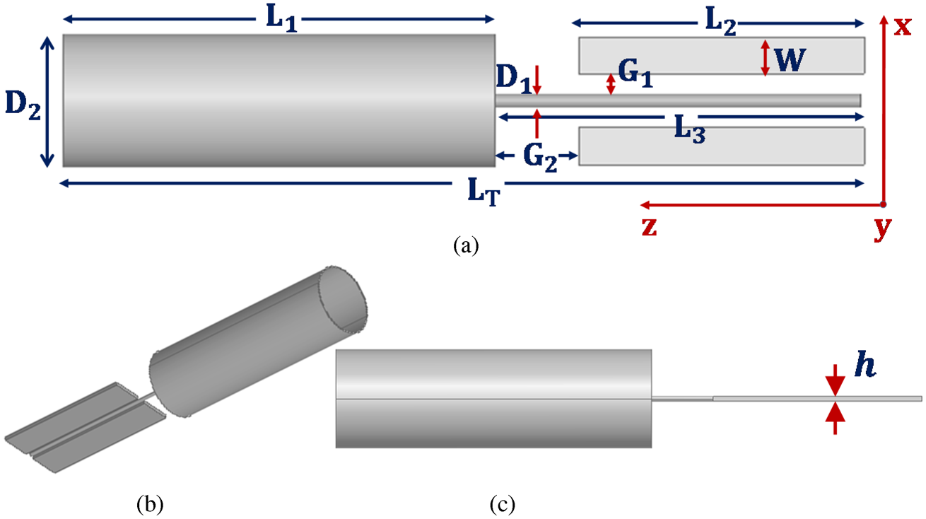
Fig. 1. CPW-fed sleeve antenna structure composed of a CPW feed line connected to a metal cylinder as the main radiating element: (a) top view, (b) 3D view, and (c) side view.
The most important design parameters of this antenna include the gap between the line and ground plane in the CPW feed section specified by G 1 and the one between the antenna's feed section and cylindrical radiating element which has been shown by G 2. The other design parameters are illustrated in Fig. 1.
In the following, the influence of these parameters on the antenna's impedance bandwidth is investigated through conducting several simulations. All of the simulated results have been obtained using the high frequency structure simulator (HFSS) software which is based upon the finite element method.
It should be said that the bandwidth evaluation criteria for all of the presented results is VSWR < 3. Using several simulations, Fig. 2 illustrates the effect of changes in the values of G 1 and G 2 on the antenna impedance bandwidth. The simulation results indicate that G 1 which controls the characteristic impedance of the CPW transmission line, affects the matching rate (VSWR value) over the whole antenna's bandwidth. On the other hand, G 2 can control the impedance bandwidth of the antenna in the higher edge frequency, so that the bandwidth starting frequency is not affected.

Fig. 2. Simulated VSWR characteristic for various values of (a) G 1 and (b) G 2.
The effect of changes in the D 1 parameter is shown in Fig. 3. Similar to G 1, this parameter can also change the characteristic impedance of the CPW transmission line and adjust the matching rate. In fact, with increasing and decreasing D 1, the capacitive and inductive property of the CPW transmission line is changed which yields the impedance matching variation, as a consequence.

Fig. 3. Simulated VSWR characteristic for various values of D 1.
Figure 4 represents the impedance bandwidth variation with changes in L 1. Simulations illustrate that L 1 basically affects the higher edge frequency, so that the matching frequency decreases at the end of the band as L 1 increases. This parameter has no significant effect on the matching of the antenna.

Fig. 4. Simulated VSWR characteristic for various values of L 1.
It is noteworthy that in all the simulations performed for the different values of the above parameters, the overall length of the L T antenna is constant. In other words, the bandwidth increase of this antenna has not been accompanied by the antenna length increment. Generally, the overall dimension of the antenna which is a function of the two parameters of L T and D 2, solely specifies the beginning frequency of the antenna's impedance bandwidth.
In all of the performed simulations in Figs 2–4, when the effect of each of the four parameters is investigated, the other three are considered to be constant. For example, when G 1 is considered, G 2, D 1, and L 2 must be kept constant. The other design parameters of the antenna in Fig. 1 such as L 2, W, and L 3 are functions of the four main parameters (L 1, D 1, G 1, and G 2). By increasing D 1, W must be reduced due to the parameters such as G 1 and D 2 which have been considered to be constant. After performing the above simulations, the optimized dimensions of the antenna are given in Table 1.
Table 1. Optimum dimension of the proposed antenna

After obtaining the antenna optimum design parameters, it simulated and the input impedance of the antenna has been achieved. The real and the imaginary parts of the input impedance illustrated in Fig. 5. The imaginary part of the input impedance shows that the antenna in the operation bandwidth has four resonances i.e. two series and two parallel resonances (see Fig. 5(b)). The simple equivalent circuit model for simple dipole antenna consists of series RLC [resistor (R), inductor (L), capacitor (C)] elements and the first resonance is due to it. It is shown in Fig. 6 in part one. The other part added in sequence to create the next resonances (see Fig. 6). The value of the inductor and the capacitor computed based on the resonance frequency and the resistances control the peak value in the real part. The comparison of the antenna input impedance and the equivalent circuit model is illustrated in Fig. 5 and shows good agreement.

Fig. 5. Comparison of the input impedance of the antenna with the equivalent circuits model: (a) real part and (b) imaginary part.

Fig. 6. Equivalent circuits model of the antenna.
Figure 7 shows the simulated surface current of the antenna at 139, 350, and 570 MHz respectively. It is clear that by increasing the operation frequency, the current phase changes along the antenna length. As shown in figure, there is one and two current phase changing at 350 and 570 MHz respectively. As we know, the number of radiation pattern lobes begins to increase due to the current phase changing which has been shown in Fig. 8(a).

Fig. 7. Current distribution on the proposed antenna: (a) 570, (b) 350, and (c) 139 MHz.

Fig. 8. Radiation patterns of E θ-component: (a) E-plane and (b) H-plane.
Figure 8 shows the radiation pattern of the simulated antenna in E and H-planes and for three different frequency values. The radiation pattern has been simulated by the FEKO simulator to validate the HFSS simulator result. As would be observed from this figure, it is clear that the proposed antenna has the same pattern as a monopole one in the E-plane and also the pattern is omnidirectional in the H-plane.
The variation of the maximum and azimuth antenna gain is plotted in Fig. 9 over the frequency. As can be seen, the gain is positive at all covered frequency bandwidth and the maximum gain is about 3.68 dBi at 0.345 GHz.

Fig. 9. The azimuth and peak gain of the proposed antenna.
Figure 10 shows the variation of the radiation efficiency over the frequency. The figure indicates that the antenna has a high efficiency that promising around 99%.

Fig. 10. Radiation efficiency of the proposed antenna.
Experimental verifications and antenna comparison
In order to validate the simulation results, an antenna prototype is fabricated according to the dimensions given in Table 1. Figure 11 represents the results obtained via the simulation and measurement of the fabricated antenna. As can be seen from this figure, good agreement has been achieved and indicates VSWR < 3 for this antenna within the frequency range of 127–586 MHz. Figure 12 shows the schematic view of the fabricated antenna.

Fig. 11. Measured and simulated VSWR for the proposed antenna.

Fig. 12. Photograph of the proposed antenna.
Table 2 gives a comparison of the proposed antenna with that introduced by previous research studies from the dimensions and impedance bandwidth point of views. Regarding the items mentioned in this table, the proposed antenna dimensions are smaller in size compared to the dimensions of the similar antennas with a similar impedance bandwidth.
Table 2. Comparison with other antennas

Conclusion
The novel wideband CPW-feed sleeve antenna was numerically and practically investigated and due to its flexible structure, all of the antenna's parameters were tuned to achieve a bandwidth of about 129% for a VSWR of less than 3, compact size of 0.274λ × 0.047λ, and higher than 90% radiation efficiency. In this regard, the simulation results were shown based on the parameters tuning and the reason for each of the effects explained as well. The omnidirectional behavior of the antenna pattern has also been shown in three frequencies over the bandwidth. Eventually, the agreement was observed between the measurement and simulation results and the comparison was also made with the other works. As a result, this antenna provided the three main features including the high bandwidth, compact size, and omnidirectional pattern therefore, it could be used for any application which needs all of these in a simultaneous manner.
 Peyman Hasani was born in Tehran, Iran, in 1993. He received his B.S. degree in 2015 from the University of Arak and received his M.Sc. at the Shahid Rajaee Teacher Training University in 2019.
 Seyed Mohammad Hashemi was born in Tehran, Iran, in 1983. He received the B.Sc., M.Sc., and Ph.D. degrees in Electrical Engineering from the Iran University of Science and Technology (IUST), Tehran, Iran, in 2006, 2008, and 2013 respectively. From 2012 to 2013 he joined Aalto University, Finland, as a Visiting Scholar. Since 2015, he is an Assistant Professor of Communications Engineering at the Department of Electrical Engineering, Shahid Rajaee Teacher Training University, Tehran, Iran. His research interests include Applied Electromagnetics, Optimization Methods, Antenna and Microwave Engineering.
 Javad Ghalibafan received the B.S. degree from the Ferdowsi University of Mashhad in 2007 and the M.S. and Ph.D. degrees from Iran University of Science Technology in 2009 and 2013, respectively. In 2014 he joined Department of Electrical Engineering, Shahrood University of Technology, Shahrood, Iran, where he is now Associate Professor, and the head of Antenna & Microwave Lab. His research interests include the analysis, design, and measurement of artificial electromagnetic materials; antenna and microwave devices; metamaterial; and magnetic material.


