Introduction
Many current and future microwave systems employ various beamforming techniques to facilitate their proper operation. Typical examples are communication systems, radar systems, and electronic warfare systems. To achieve the beamforming function, the key element used is a phase shifter. For a wideband system, the phase shifter must be replaced by a TTD (true time delay) component to prevent beam-squinting [Reference Ghaderi, Ramani, Rahimi, Heo, Shekhar and Gupta1]. As a result, many approaches have been developed for the implementation of TTD [Reference Ghaderi, Ramani, Rahimi, Heo, Shekhar and Gupta1–Reference Hu and Mouthaan11].
Approaches based on transmission lines [Reference Carosi, Cesarotti, Lasaponara, Marescialli and Rapisarda2, Reference Tian, Lee and Wang3] or artificial transmission lines based on LC structures [Reference Chu, Roderick and Hashemi4, Reference Cho, Han, Kim and Kim5] yield large size at 2–18 GHz frequency range and high loss and delay variation over the frequency band. It may become a more attractive solution only at a higher frequency [Reference Ma, Leenaerts and Baltus6, Reference Park and Jeon7]. RC structures are quite small, but they are very lossy. The use of analog and discrete time delay approaches exhibit high accuracy and small size at the expense of power consumption linearity and frequency BW limitation [Reference Ghaderi, Ramani, Rahimi, Heo, Shekhar and Gupta1, Reference Garakoui, Klumperink, Nauta and van Vliet8, Reference Zolkov, Madjar, Weiss and Cohen9]. More recent publications present some new results in the design of TTD. Jung et al. [Reference Jung, Yoon and Min12] have developed a 3-bit TTD operating in the range 8–24 GHz. Their approach is based on a variation of APN networks. Their max delay is around 50 ps. Their chip is small but quite lossy. The same group [Reference Jung and Min13] has also developed a 4-bit TTD in the range of 3–30 GHz with a max delay of 68.5 ps based on a similar approach to their other design. The loss of this chip is quite high (13.5 dB) with an rms delay error of 2 ps. Lee et al. [Reference Lee, Cho and Hong14] reported a 5-bit TTD in the range 20–30 GHz with a max delay of 36.9 ps. This design is based on the concept of “dual-sided microstrip line”, which reduces the size of the chip (0.07 mm2). However, the loss is quite high (7–20 dB). Mandal et al. [Reference Mandal and Mandal15] have developed two TTD circuits on a PCB, one in L band (single bit) and one in S band (3-bit). They used an approach of “periodic shunt open stubs”. This approach yields low loss (1.9 dB at 3 GHz), but the circuit is very large (70 × 10 mm2). Max delay is 84 ps. Our approach presented below is based on all-pass networks (APN) [Reference Willms, Ouacha, de Boer and van Vliet10, Reference Hu and Mouthaan11] with the first three bits implemented in a single delay cell, aimed at reducing the size and delay variation over the microwave band. Bits 4 and 5 are implemented using APN delay cells and SPDT switches, which is the common practice. However, bits 1, 2, 3, and 6 are designed by using novel approaches as explained below. In addition, our design includes a buffer amplifier between bits 4 and 5. The amplifier provides isolation between the two parts of the chip. This improves dramatically the delay error, and also provides some peaking to partially compensate for the increase of loss with frequency.
This paper is organized as follows: section “Modified APN” includes the schematic, theory, and design equations for an APN delay cell [Reference Feng16]. In addition, modified APN is described, which we use to implement the first three bits in a single delay cell. Section “TTD design” contains the design of all six bits of the TTD as well as the design of the buffer amplifier inserted between bit 4 and bit 5. The simulated and measured performance of all 64 states is presented in section “Simulated and measured performance”. Section “Conclusion” includes the conclusions.
Modified APN
An analysis of APN is presented in section 4.2 of [Reference Feng16]. These networks are superior in terms of size and transmission loss per delay. In this section, we present briefly the classical APN as well as our new suggestion for a modified APN, which permits the implementation of 3 bits in a single delay cell.
Classical APN
The circuit of a second-order APN is presented in Fig. 1. A classical network is depicted in (a) and our modified network is depicted in (b).

Fig. 1. A second-order all-pass network (a) classical; (b) modified (M-mutual inductance).
By proper design, the classical network can be ideally matched at both ports and the transmission magnitude is 1 (0db) at all frequencies (all pass). The conditions for perfect match and transmission are:


Z 0 is the port impedance.
In general, the group delay of this circuit varies with frequency; however, by plotting the curve of the group delay versus frequency with a parameter, Q [Reference Feng16]:

One finds out that for Q = 0.1, the group delay is almost constant and equal to the low-frequency delay, τ 0:

Over the frequencies from DC to ωmax:

The above equations can be used to calculate the circuit elements (L, M, Cs, Cp) to obtain the desired group delay and bandwidth. Equation (5) represents the relation between the maximum possible delay with this circuit for the desired bandwidth. For example, if the desired bandwidth is 20 GHz, the maximum possible delay is 16 ps.
Modified APN
As shown in section “TTD design”, a TTD bit can be obtained by using the all-pass circuit above along with two single-pole double-throw (SPDT) switches that switch the signal path between a direct transmission from input to output and a path through the delay cell. To reduce the size of the chip, we combined the first three bits (least significant bit (LSB)) into a single modified APN cell as shown in Fig. 1(b).
The circuit in Fig. 1(b) has the topology of an ordinary APN; however, instead of fixed capacitors here we use variable capacitors to obtain variable delay. Since for an APN, an ideal matching is possible only for a single design that corresponds to one delay value, for the other delay values, there will be some mismatch. The design of the modified APN cell is a tradeoff between bandwidth, matching and delay, and it follows the procedure:
-
Step 1: design the cell for a given delay value with perfect matching using equations (1)–(5).
-
Step 2: repeat step 1 for a few values of delay τ 0 (in the case of bit 1–3, we can select values in the range 10–20 ps).
-
Step 3: for each one of the cases in step 2, calculate the maximum delay variation over the band, the maximum return loss over the band, and the range of values for Cp. This can be done by using the equations in [Reference Feng16], which are repeated here:
(6)$$Z_{in, e} = \displaystyle{{1-\omega ^20.5C_p( {L + M} ) } \over {\,j\omega 0.5C_p}}, \;$$ (7)$$Z_{in, o} = \displaystyle{{\,j\omega ( {L-M} ) } \over {1-\omega ^22C_s( {L-M} ) }}, \;$$(8)$${\rm \Gamma }_{in, e} = \displaystyle{{Z_{in, e}-Z_0} \over {Z_{in, e} + Z_0}}{\rm \;}{\rm \Gamma }_{in, o} = \displaystyle{{Z_{in, o}-Z_0} \over {Z_{in, o} + Z_0}}, \;$$(9)$$S_{11} = 0.5( {{\rm \Gamma }_{in, e} + {\rm \Gamma }_{in, o}} ) {\rm \;}S_{21} = 0.5( {{\rm \Gamma }_{in, e}-{\rm \Gamma }_{in, o}} ) .$$
 -
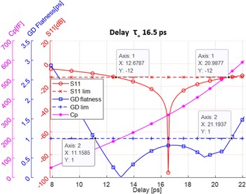
Step 4: for each of the cases in step 2 (based on the calculations in step 3), plot a composite graph as shown in Fig. 2. The plots in this figure depict three variables (max S 11 in the frequency band, delay fluctuations in the frequency band, and the value of Cp) as the function of the cell delay. The plots demonstrate the tradeoff between impedance matching, delay variations, and cap values.
-
Step 5: review all the plots in step 4 and select the design with the best tradeoff based on delay and S 11 limits defined. In Fig. 2, we can see that this design allows delay change from 11.1 to 21.1 ps (more than the required span of 7 ps for bit 1–3). In that range, the maximum delay variation over the band 2–18 GHz is 1 ps, the minimum return loss is 12 db over the delay range of 12.5–21 ps. This design was selected for our bit 1–3. If we select a larger matched delay (step 2), the bandwidth is reduced due to higher delay; if we select a lower matched point delay, the bandwidth is reduced due to narrower band of S 11, S 22. This is shown in Table 1.
-
Step 6: for the selected optimum design, simulate the circuit and optimize it to obtain the best possible performance in terms of input and output return loss, the desired eight delay states and the needed span of the serial and parallel capacitances.


Fig. 2. A composite plot showing Cp range sweep, max S 11, and delay variation over the band for optimal case-matched delay cell of 16.5 ps.
Table 1. Comparison of different ranges for modified APN

TTD design
In this section, the design of the TTD chip and its six bits is presented.
The TTD chip block diagram
The block diagram of the TTD chip is depicted in Fig. 3.

Fig. 3. Block diagram of the complete TTD chip.
As can be seen in Fig. 3, the TTD chip includes a cascade of five units: one cell implementing bits 1–3 (eight delay states), one cell implementing bit 4, a buffer amplifier, bit 5, and bit 6. The design of each one of these units is detailed below. The need for the buffer amplifier and its location in the chain to minimize mismatch is also explained in section “Buffer amplifier requirement”. All designs were performed by keysight Technologies ADS. The layout and final simulation used Cadence's Virtuoso.
Bits 1–3
Bits 1–3 are implemented as a single composite delay cell based on the modified APN in Fig. 1(b). The cell is intended to act as a 3-bit delay line, namely, eight delay states. The lower state is the reference (state 0), state 1 has a delay of the reference plus 1 ps, and state 8 has a delay of the reference plus 7 ps. The design of this cell is obtained following the procedure outlined in section “Modified APN”, and a compromise is achieved between delay requirements, impedance matching, and capacitance values. The optimal design was found to be for a nominal matched delay of 16.5 ps as depicted in Fig. 2. From this plot, we can see that a delay span of about 10 ps can be obtained with a delay ripple of <1 ps and worst-case return loss of 12 dB. The corresponding required change of Cp is from about 100 to 400 fF, which is a practical range (the corresponding Cs values are from 10 to 40 fF – equation (3)).
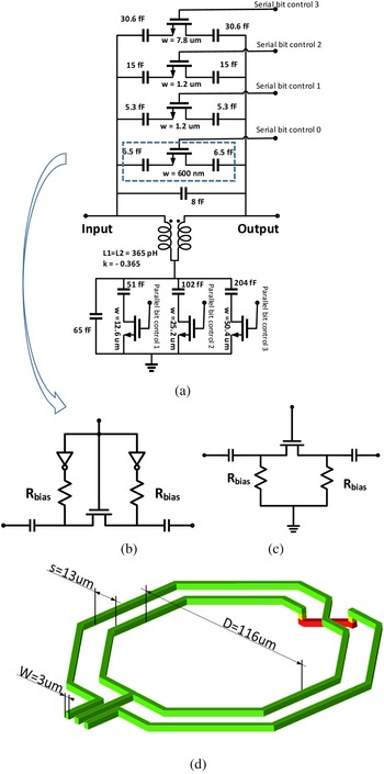
The actual implementation of the delay cell is depicted in Fig. 4. This circuit has the topology of an ordinary APN; however, instead of fixed series and parallel capacitors, banks of switched capacitors are used. The series cap bank includes nine fixed caps switched by four transistors. The parallel cap bank includes four fixed caps switched by three transistors. The eight delay states (0–7 ps) are obtained by eight switching combinations of the switching transistors. For each state, the effective series and parallel capacitances are set, such that the delay difference between consecutive states is 1 ps. The layout of the coupled coils is depicted in Fig. 4(d). Note that the distance between the strips is relatively large (13 μ). This is needed to implement the relatively small coupling coefficient (k = −0.365). The crossover between the turns of the coil is needed to implement the negative coupling coefficient. All transistors are 65 nm RF transistors (TSMC_CM065_2V5_NMOS_RF). Gate periphery of each transistor (W) is marked in Fig. 4(a). This type of transistor is used for all the designs.

Fig. 4. (a) Modified all-pass network schematic for bits 1–3 (k-coupling coefficient); (b) switch with inverter units; (c) switch without inverter units; (d) coupled inductors.
The implementation of three bits in a single delay cell has several advantages: (a) substantial size reduction compared to three separate cells; (b) the insertion loss is much lower compared to three separate cells; (c) capacitance banks allow accurate tuning of the delay, including the possible partial correction of errors of the other bits (option of calibration table for the complete TTD). As shown in Fig. 4, the series capacitance bank includes four switching elements. Since this unit is a 3-bit cell, the four switches allow a degree of freedom, which can be used for the tuning of the delay curve to obtain a better fit to the desired response. This capability is demonstrated in Fig. 5, which depicts the absolute delay response of this cell over the frequency band with several settings of the four switches. This capability can be used for the complete TTD chain to tune the delay curve by establishing a calibration table.
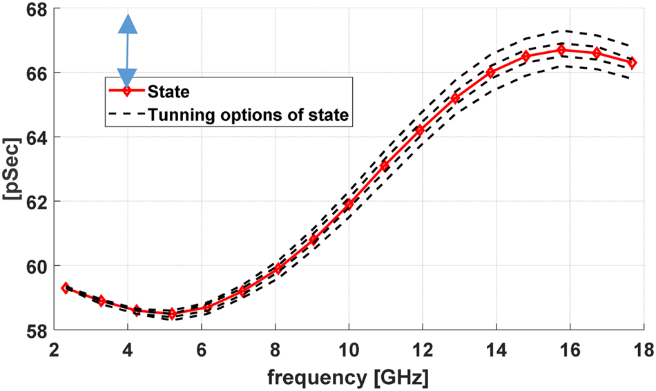
Fig. 5. Fine tune the delay curve of bits 1–3 for one of the states.
Two options were considered for the switching of the series cap bank of Fig. 4(a). One biasing arrangement is depicted in Fig. 4(b), which includes inverter units. A second arrangement is depicted in Fig. 4(c), which does not include inverter units. The biasing without inverters requires very large parallel resistors to avoid loading to the ground, which deteriorates the performance of the switch. On the other hand, when using the inverter units, their high impedance allows the use of much smaller resistors (5 Kohm). Thus, we decided to use the arrangement with the inverters for bits 1–3. This effect is demonstrated in Fig. 6, which depicts the variation of the group delay for both cases with several resistor values. From Fig. 6, for the case of no inverters, the group delay is dependent on the resistor value and changes over the frequency band. On the other hand, when inverters are used, the group delay is almost constant over the frequency band and practically independent of the resistor value.

Fig. 6. Group delay dependence on bias resistors of series cap switch bits 1–3.
Bit 4
Bit 4 switches the signal between 0 and 8 ps. The schematic of bit 4 is presented in Fig. 7(a). Due to the parasitic capacitance of the inductor, the optimized value of the series cap of the APN cell is very small (<1 fF), so in practice the series cap is not needed.
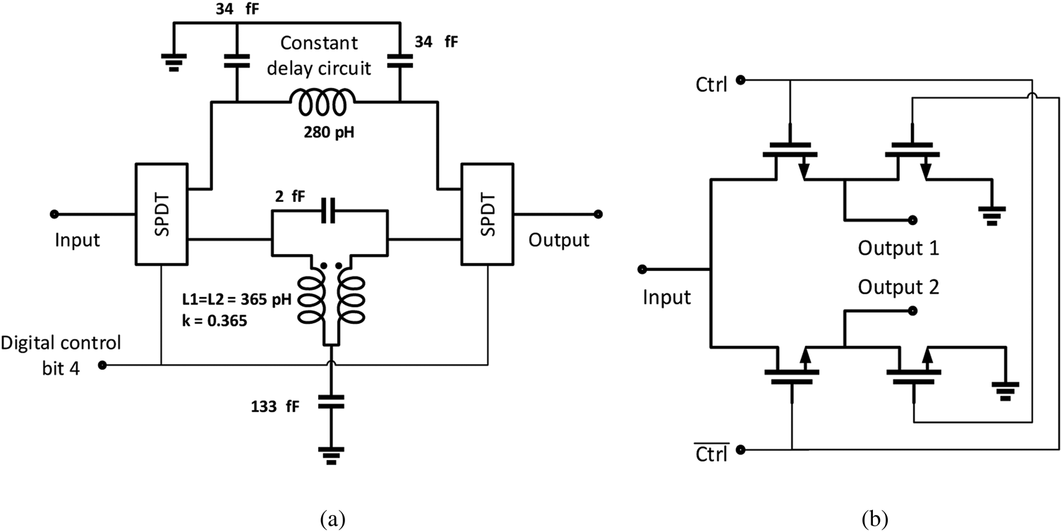
Fig. 7. (a) Schematic of bit 4; (b) schematic of SPDT switch.
The topology of bit 4 is the conventional topology of a delay bit [Reference Cho, Han, Kim and Kim5, Reference Willms, Ouacha, de Boer and van Vliet10] namely, two SPDT switches are switching the signal path between a direct (no delay) state and a delay path state. The delay path is an APN designed using the same inductor as in bits 1–3. The resulting average delay is around 17 ps. The CLC circuit at the top is a fixed delay of 9 ps used to compensate for the excess delay of the delay path. The CLC circuit is also used to absorb the parasitic caps of the switches, which improves the matching. Thus, the resulting bit is an 8 ps delay bit.
An SPDT switch schematic is presented in Fig. 7(b). Each branch of the SPDT includes one series and one parallel transistor. The size of the transistors is determined as a compromise between loss and isolation. The initial design uses relatively large series transistors with ON resistance around 5 ohm to reduce loss, while the parallel transistors are smaller to avoid large OFF capacitance. After optimization, our design provides an isolation of 30 db and a loss of 0.5 db. The optimized series transistor has a gate periphery of 85[sym]-3987_Symbol[/sym]m and the parallel transistor 7[sym]-3987_Symbol[/sym]m.
Bit 5
Bit 5 switches the signal between 0 and 16 ps. The schematic of bit 5 is presented in Fig. 8. The topology of bit 5 is the same as bit 4, except that the delay cell is designed for 16 ps using the same inductor without bypass delay. Bits 4 and 5 are expected to have good impedance matching at the ports since both the SPDT switches and the delay cell are theoretically perfectly matched.

Fig. 8. Schematic of bit 5.
Bit 6
Bit 6 switches the signal between 0 and 32 ps. As explained in section “Modified APN” above, a second-order APN can be designed for a maximum delay of 16 ps over the frequency band up to 20 GHz. This means that bit 6 cannot be implemented by a single delay cell of the type used for bit 4 and bit 5. Bit 6 implements the 32 ps delay by using two delay cells in cascade. To obtain the desired delay and good impedance match, one needs to use two structures of bit 5 in cascade. However, to save two SPDT switches and reduce the chip size, we cascaded the two APNs without intermediate SPDTs (Fig. 9) and optimized the design to obtain both the desired delay difference and a reasonable impedance match.

Fig. 9. Schematic of bit 6.
Buffer amplifier requirement
The six TTD bits described above can be divided into two categories: (1) bit 4 and bit 5 – conventional design based on APN and SPDT switches; (2) bit 1–3 and bit 6 – modified APN. The bits of category 1 exhibit good impedance matching (return loss >17 dB), while the bits of category 2 exhibit some impedance mismatch (return loss >12 dB). As a result, when cascading all the bits without any buffers, the performance is severely degraded. One effect of the impedance mismatch between the bits is a substantial mismatch at the input and output. More important, the mismatch between the bits causes severe degradation of the delay response although the delay response of each bit by itself is very good. This effect can be understood from the fact that the delay is basically the derivative of the phase response. So even a reasonable error of the phase (due to impedance mismatch) translates into a large error in delay.
We have investigated this problem by initially inserting an ideal isolator between each pair of bits. The delay performance of the chain with the ideal isolators was excellent. Then we considered what type of practical isolator to include in the design and the minimum number of isolators to obtain reasonable performance. After investigating several cascading possibilities, we concluded that it will be enough to use only one buffer amplifier inserted in the chain between bit 4 and bit 5. We paired a delay cell of category 1 with category 2 and separated the pairs with the buffer – section “Simulated and measured performance” shows a comparison between the case of with and without a buffer.
Another benefit obtained by inserting the buffer amplifier is some gain to compensate for the natural loss of the practical bits. In addition, since the loss of the practical delay bits has a negative frequency slope, we decided to design a peaking amplifier, which has a positive frequency slope. Thus, the buffer amplifier helps in solving the isolation problem between bits, compensates for some of the loss, and reduces the frequency slope of the bits. The design and performance of the buffer amplifier are described in section “Buffer amplifier design and performance”. The specification of the buffer amplifier was determined by simulating the complete TTD with an almost ideal buffer having finite isolation, some mismatch, and some frequency peaking. The above parameters were tuned to obtain a reasonable performance of the complete chain. As a result, the following spec is set for the buffer amplifier (Table 2)
Table 2. Buffer amplifier specifications

Buffer amplifier design and performance
The schematic of the amplifier is depicted in Fig. 10.

Fig. 10. Schematic of the buffer amplifier.
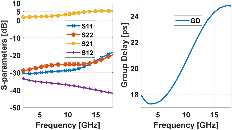
The amplifier is composed of a cascade of three inverter units with feedback. This approach is common for compact wideband amplifiers [Reference Slimane, Haddad and Bourdel17, Reference De Souza, Mariano and Taris18]. This complementary arrangement permits the use of a single positive DC voltage (1.2 V) and self-biasing. The use of resistive feedback yields a wideband amplifier over the entire 2–18 GHz band. We have used a feedback of a series RL with a small inductor to achieve the peaking effect, namely, a positive frequency slope. The design was done by optimization with the goals specified above. The simulated performance of the amplifier is presented in Fig. 11. The DC power consumption of the amplifier is 12.4 mW.

Fig. 11. Simulated performance of buffer amplifier.
The data in Fig. 11 show that the design goals have been met: isolation >30 dB, a magnitude of S 11, S 22 lower than −18 dB, a small positive gain slope of about 3 dB. The noise figure of the amplifier is 11 dB, and the 1 dB compression is −5 dBm at the output. This amplifier was inserted between bit 4 and bit 5 of the TTD chain. The amplifier has some dispersion (change of delay with frequency), but it is acceptable for most applications.
Simulated and measured performance
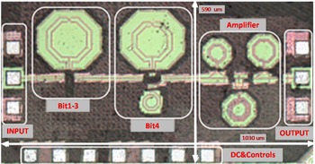
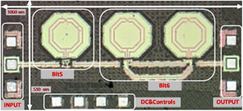
The 6-bit TTD covering the band 2–18 GHz has been implemented as an RFIC chip using the TSMC 65 nm technology. To facilitate proper analysis, testing, and debugging, and to investigate isolation impact, we have split the chip into two parts: one chip includes bits 1–3, bit 4, and the buffer amplifier (1 × 0.6 mm2), the second chip includes bit 5 and bit 6 (1.1 × 0.5 mm2). The splitting of the chip permits the separate testing of each part and the investigation of the isolation impact. The S parameters of each part are measured and combined to show the complete performance. The photo of the first four bits plus the buffer amplifier is depicted in Fig. 12, and the photo of bits 5–6 is depicted in Fig. 13. In Figs 12 and 13, the various parts of the chip are marked.

Fig. 12. Photo of bits1–4 and buffer amp.

Fig. 13. Photo of bits 5–6.
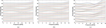
Figure 14 shows the simulated and measured delay difference versus frequency for the combined bit 5 + bit 6. There are four delay states: 0, 16, 32, 48 ps. Controlling the digital inputs in both chips is done using the internal serial data interface and an Arduino UNO microcontroller.

Fig. 14. Simulated and measured delay response for bit 5 + bit 6.
The measured results agree quite well with the simulations; they are very close to the desired performance. The return loss at input and output is better than 10 dB over the band. The insertion loss varies between 3 and 7 dB over the frequency range and all four delay states. The RMS delay error at each frequency over all four states has been calculated. The results are depicted in Fig. 15. The RMS delay error is calculated by:


Fig. 15. RMS error of delay for bits 5–6 (calculated from measurement).
TD 0 – reference delay, TDi – state i delay, ΔTDstep – nominal delay step between states, ΔTDrms – average rms delay error, N – number of states.
The delay performance of the combination bits 1–3 + bit 4 + amplifier is depicted in Fig. 16 (simulated and measured). There are 16 delay states (0, 1, 2, …., 15). The measured and simulated results agree in general. The RMS delay error at each frequency over all 16 states has been calculated. The results are depicted in Fig. 17.

Fig. 16. Simulated and measured delay for bits 1–4 (2–18 GHz).

Fig. 17. RMS error of delay for bits 1–4 (calculated from measurement).
For bits 1–4, the return loss at input and output is better than 10 dB over the band. The insertion loss varies between 1 dB up to the gain of 2.5 dB over the frequency range of all 16 delay states.
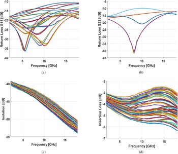
Now we look at the performance of the complete TTD including the 6 bits and the amplifier (the two measured chips combined). There are 64 delay states: 0, 1, …., 63 ps. For the complete TTD, the return loss at input and output is better than 10 dB (Figs 18(a) and 18(b)), the isolation between output and input is more than 38 dB (Fig. 18(c)), and the loss varies between 2.5 and 6.3 dB (Fig. 18(d)). The input 1 dB compression point of the complete TTD is −3 dBm – limited by the amplifier.

Fig. 18. Simulated (a) S 11; (b) S 22; (c) S 12; (d) S 21 of the complete TTD chip using measured data of the individual chips.
The RMS delay and amplitude error of the actual TTD is depicted in Fig. 19. The delay error has been calculated by using equations (10) and (11). The amplitude error has been calculated by equation (12):

where Amp avr is the average amplitude over all 64 states.

Fig. 19. RMS delay and amplitude error for the complete TTD (calculated from measurement).
The complete chip exhibits a delay variation of 1.1 ps up to 15 GHz, which is 1.6% of the max delay span (64 ps). At the higher end (15–18 GHz), the delay error increases. The amplitude of RMS error over the entire band is <1 dB. Table 3 contains a comparison of the performance of our chip with similar published chips, showing the improved gain and delay variation with small size.
Table 3. Performance comparison of TTD chips

The delay response of the TTD chip is shown in Fig. 20. The figure includes three delay responses versus frequency for all 64 states. The responses were obtained by cascading the measured chips in an ADS schematic. The three response figures were obtained as follows: Fig. 20(a) is the response of the actual complete TTD, namely, the cascade connection of the first chip (bits 1–3, bit 4, amp) and the second chip (bit 5, bit 6). Figure 20(b) is the response of the cascade of the first chip, an ideal isolator (ADS model – ideal matching and infinite isolation) and the second chip. Figure 20(c) is the response of the cascade of the second chip followed by the first chip. This is equivalent to TTD without buffer since the buffer amp is located at the end of the first chip. Comparing the graphs in Fig. 20, we can conclude: (1) TTD without buffer has very poor performance, as expected; (2) the performance of the TTD with the practical buffer amplifier is very close to the TTD with ideal isolator. This means that the buffer amplifier matching and isolation is sufficient.

Fig. 20. Simulated delay response for the complete TTD using measurements of individual chips (a) with buffer amplifier, (b) with ideal buffer, (c) no buffer.
Conclusion
In this paper, we have presented the design, simulation, and measurements of a 6-bit TTD chip implemented in TSMC 65 nm technology. The chip is very wideband and covers the band of 2–18 GHz. The LSB is 1 ps and the sixth bit is 32 ps. The design of the various bits is based on APN and modified APN, which are known to exhibit constant delay over a large bandwidth. The first three bits were implemented in a single switchable delay cell reducing size, loss, and delay variation compared to the cascaded bits approach. The chip includes also a peaking buffer amplifier based on inverter units with inductive feedback to reduce delay variation and compensate for frequency response loss. Full TTD has <1.6% delay variation and 1 dB RMS amplitude variation over the frequency band.
Acknowledgements
The authors would like to thank the Israeli MOD for supporting this work.
 Yakov Gutkin received his M.Sc. degree in Electrical Engineering from Technion – Israel Institute of Technology, Haifa, Israel, in 2020 and the B.Sc. degree from ORT Braude College, Carmiel, Israel in 2011. From 2010, he has been working for Intel Israel as an RF chip designer. After completion of his M.Sc. thesis, he continues to work for Intel Israel.
 Asher Madjar (IEEE Life Fellow) received his D.Sc. degree from Washington University in St. Louis in 1979 and the B.Sc. and M.Sc. degrees from the Technion – Israel Institute of Technology in 1967 and 1969, respectively. Dr. Madjar's expertise is in the area of microwave and microwave photonics components, integrated circuits, and subsystems. He has been working for more than 50 years in the field of industry and teaching in academia both in Israel and the USA. He performed research in many aspects of this field, and has published over 150 papers in the professional magazines and in conferences. In this industry, he established several key know-how centers (MIC laboratory, MMIC design group) and trained generations of microwave engineers in Israel. His current interest is in advanced technologies for microwave and microwave photonics hardware: monolithic integration, THz devices, wide band gap devices, optical/microwave interaction, advanced design techniques, etc. Dr. Madjar became a member of IEEE in 1972. He is a Life Fellow of IEEE since 2011, and an IEEE Fellow since 1997. He has been involved in the instruction of many graduate students both in Israel and the USA. He is one of the founders of the European Microwave Association and has been involved heavily in restructuring the European Microwave Conference and European Microwave Week. He served on the first Board of Directors of the European Microwave Association. He is a member of the TPC of both the IEEE International Microwave Symposium and the European Microwave Conference. He was the chairman of the European Microwave Conference in 1997 (Jerusalem). He received the “Best Researcher Award” from RAFAEL, Israel in 1997. Dr. Madjar was involved heavily in IEEE activities in Israel, both in the section level and the AP/MTT chapter, which he established in 1973 and served as its chairman for many years. Presently, Dr. Madjar is an independent consultant. Occasionally, he teaches in the USA as well as Israeli universities. He is also involved in research activities at the Technion in Israel.
 Emanuel Cohen received the B.Sc., the M.Sc., and the Ph.D. degrees in Electrical Engineering from Technion, Haifa, Israel, in 1996, 2002, and 2012, respectively. He worked 9 years on military communication systems as the head of the RF department. In 2004, he joined Intel Israel, where he was involved with WiFi and WiMAX systems, defining and developing the RF-integrated circuits (RFICs) and algorithms for these standards, including calibrations for BIST systems, linearization, and efficiency enhancement for PAs. Since 2015, he is an assistant professor at the Technion Institute of Technology in Israel. His current research areas include high-frequency beamforming arrays in advanced CMOS process and integrated mixed signal concurrent systems for frequency-division and full duplex.