Introduction
Nowadays, microstrip array antennas are used in a large number of wireless applications such as cellular, satellite communications, radar and high speed wireless local area network (WLAN) due to the inherent usefulness of low cost, low profile, light weight, easy fabrication process, and easy integration with active devices. In addition, circular polarization (CP) microstrip array antennas have received attention not only due to gain enhancement, but also the benefit of avoiding polarization losses. When polarization matching is not necessarily assured for a given orientation of linearly polarized transmitter and receiver antennas, it is preferable to use CP. This is the case, for example, with low earth orbit or unstabilized satellites, where the antennas are randomly oriented. Therefore, an attempt is taken in this study to design a compact CP array antenna for achieving high gain using a multi-layer structure compared to a single layer structure. It is also considered to make the layout easy to design and fabricate by integrating simple structure.
The basic concept to generate CP is to produce two orthogonal near degenerate modes on the patch where the quadrature phase shift exists between the two modes [Reference Maci, Gentili and Avitabile1]. Therefore, this concept can be fulfilled by either creating perturbation in the patch or using two orthogonal feed points on the patch. Many research works have been reported on various perturbation types CP single patch antennas, such as truncated corner patch antennas [Reference Tang, Lu and Wong2,Reference Chen, Wu and Wong3], U-shaped slot antenna [Reference Xu, Li, Yang, Wei and Qi4], E-shaped [Reference Khidre, Lee, Yang and Elsherbeni5] and half E-shaped [Reference Kovitz, Rajagopalan and Rahmat-Samii6] patch antennas, and patch antennas loaded with shorting pins [Reference Zhang and Zhu7]. CP array antennas using different feed network structures have also been investigated. Corporate feed [Reference Lu and Chang8,Reference Choi, Pyo and Choi9] and series feed [Reference Pozar and Schaubert10–Reference Evans and Sambell12] network arrangements are two possible ways to configure array antennas. Generally, the performance is degraded in corporate feed arrangements due to their longer feed length, whereas series feed networks show simple and compact structure [Reference Hall and Hall13]. In [Reference Chen, Huang and Hsu14], a T-shaped CPW-to-slot lines feeding structure has been proposed to design a circularly polarized array antenna, though the antenna shows low axial ratio (AR) performance <1%. But the sequential rotation technique can be used to improve bandwidth and polarization purity for both feed arrangements [Reference Hall, Dahele and James15–Reference Li, Zhang and Feng19]. A circularly polarized antenna array with rectangular parasitic elements has been presented in [Reference Ding, Gao, Yu, Qu and Zhang20] wherein sequential rotation technique is employed to achieve broadband performance and the rectangular parasitic elements are used to enhance antenna gain. A compact series-fed CP array using coplanar proximity coupling has been presented in [Reference Chen, Fumeaux, Monnai and Withayachumnankul21] to achieve an efficiency of 90%. Another proximity coupled fed array antenna has been studied in [Reference Lo, Chan and Luk22] where the AR bandwidth is improved using an array with the sequential rotation technique compared to single element antennas. The use of linearly polarized patch elements in array configuration can be a good technique to excite CP. A CP array with linear polarization (LP) patches has been demonstrated in [Reference Huang23]. This is the first array using the sequential rotation technique to get excellent CP over a wide frequency bandwidth. But such type of antennas has a problem that the gain is reduced more than 3 dB over the whole bandwidth when the element spacing is greater than about 0.7λ 0 [Reference Hall, Huang, Rammos and Roederer24]. Two multi-layer broadband CP array antennas have been presented in [Reference So, Luk and Chan25,Reference Lai, Xue, Wong, So and Zhang26]. In [Reference So, Luk and Chan25], a truncated corner square patch array antenna designed using U-slot has been proposed where rectangular waveguide feed network is applied to obtain a good reflection coefficient (RC) over the operating band. A substrate integrated patch antenna has been realized [Reference Lai, Xue, Wong, So and Zhang26] by using three-dimensional (3-D) M-Probe feeding mechanism to obtain wide impedance bandwidth as well as broadband CP performance.
Several antenna structures [Reference Rahman, Hossain, Hossain, Nishiyama and Toyoda27–Reference Rahman, Hossain, Hossain and Chowdhury32] employing the both-sided microwave integrated circuit (MIC) technology have been proposed in the last few years. The technology gives a benefit to use various types of transmission lines such as microstrip lines, slot lines, coplanar waveguides etc. on both sides of the dielectric substrate [Reference Aikawa and Ogawa33]. A CP array using inclined LP patches [Reference Rahman, Hossain, Hossain, Nishiyama and Toyoda27,Reference Rahman, Nishiyama, Hossain, Hossain and Toyoda28], orthogonally fed slot ring array antennas [Reference Feng, Nishiyama and Aikawa29,Reference Ushijima, Feng, Nishiyama and Aikawa30], and square patch array antenna [Reference Ushijima, Nishiyama and Aikawa31,Reference Rahman, Hossain, Hossain and Chowdhury32] have been reported where feed networks are designed using series-parallel microstrip-to-slot branch circuits to take the benefits of the both-sided MIC technology. Moreover, this type of feed network provides easy impedance matching and is suitable to configure large-scale extensible arrays.
This paper proposes a new orthogonal feed 1 × 2 CP array antenna using a multi-layer structure. The both-sided MIC technology is effectively used to realize the series-parallel feed networks designed using microstrip lines and slot lines. Besides, a new 3-way power divider is also designed as a part of the feed network. A similar structure using a single layer technique has been presented in [Reference Rahman, Nishiyama, Toyoda, Hossain and Hossain34]. Adjustment of patch spacing was restricted in the single layer structure due to the placement of the feed network and patches on the same substrate plane. The sidelobe of that antenna was high due to this constraint. Therefore, the multi-layer approach is applied to the proposed antenna to improve the gain of the antenna by reducing the sidelobe level. The proposed antenna has a simpler and more compact structure than conventional array antennas as the feed network is distributed on the different layers and less impedance matching circuits are required. Moreover, it also shows good CP radiation performances with high gain. The structure and parametric analysis along with simulated and measured results are presented in the subsequent sections.
Antenna structure and design
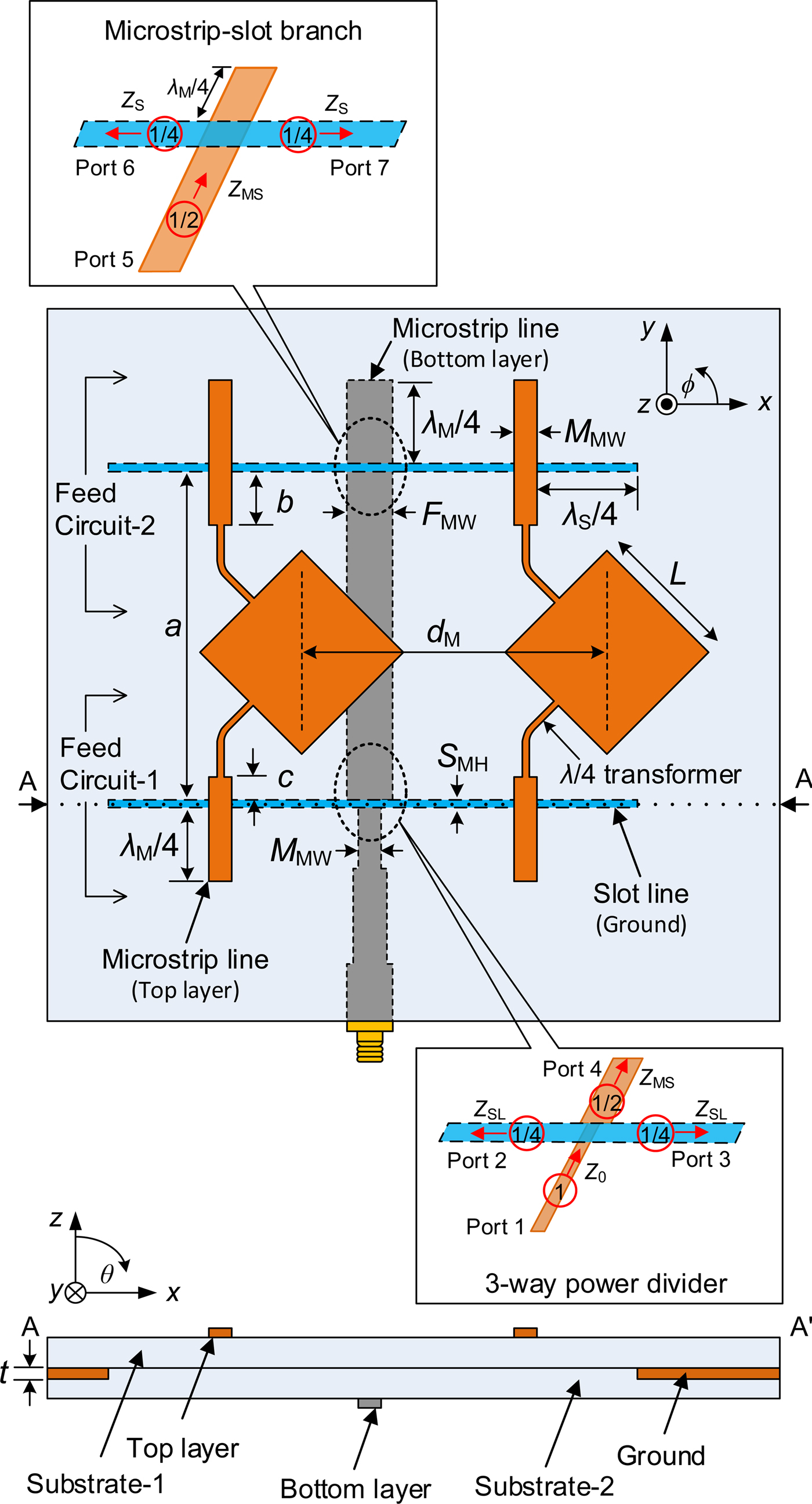
Figure 1 illustrates the schematic layout of the proposed multi-layer 1 × 2 array antenna. The antenna is designed using three metal layers separated by two 0.8-mm thick Teflon glass fiber substrates (Substrate-1 and Substrate-2) whose dielectric constant is 2.15 (according to the datasheet). The antenna consists of two square-shaped patch elements and a feed network composed of microstrip lines and slot lines. Each patch element, having a side length of L, is aligned at an angle of 45° and fed by orthogonal feed lines. The patch elements and the feed lines associated with the patches are placed on the top layer.

Fig. 1. Schematic layout and cross-sectional view (AA′) of the multi-layer structure of the proposed array antenna. Parameters are: M MW = 0.7 mm, S MH = 0.2 mm, F MW = 2.4 mm, L = 9.6 mm, and d M = 0.6λ 0 = 17.92 mm. λ M and λ S are the wavelengths for microstrip line and slot line at the design frequency of 10 GHz, respectively.
The feed network of the array is designed by using the both-sided MIC technology which enables to employ different kinds of transmission lines on both the side of the substrate. In this structure, microstrip lines and slot lines are utilized in conjunction for the feed network. Microstrip feed lines are distributed on the top and bottom layers. Furthermore, the middle layer represents a common ground where two coupling slots are placed. The feed network is divided into two parts, Feed Circuit-1 and Feed Circuit-2, to create an orthogonal feed arrangement for each patch element. Main feed line connected to a 50-Ω port is placed on the bottom layer.
Feed Circuit-1 is composed of a new 3-way power divider to divide the input power in 2:1:1. The RF power applied through the input microstrip line (Port 1) is divided into three parts at the junction. Half of the total power goes through two slot branches (Port 2 and Port 3) and remaining half of the total applied power goes through the microstrip branch line (Port 4). In this case, two slot branches (Port 2 and Port 3) on the same slot line make parallel branch and output microstrip branch (Port 4) in series with the slot branches. For effective power transfer by proper impedance matching, the slot line impedance (Z SL) should be the same as the input microstrip line impedance (Z 0) and output microstrip line impedance (Z MS) have to be half of input microstrip line impedance (Z 0) for 2:1:1 power division. The relation between the branch impedances can be expressed as follows:
 $$ Z_{\rm MS} = Z_ {\rm SL}/2, $$
 $$ Z_{0} = Z_{\rm MS} + Z_{\rm SL}/2. $$
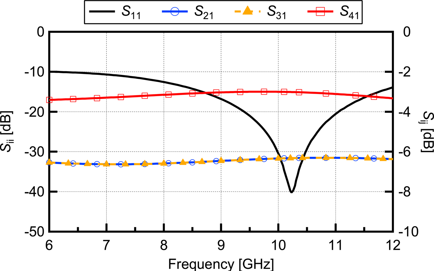
Figure 2 presents the simulated S-parameters of the proposed 3-way power divider. The 3-way power divider is designed to investigate the performance at X-band by using the branch impedances as Z 0 = 100 Ω, Z SL = 100 Ω, and Z MS = 50 Ω. This figure confirms that Port 4 receives half of the total input power (−3 dB) through microstrip branch and the remaining half is divided into two equal portions at the junction to provide quarter power (−6 dB) to Port 2 and Port 3 through two slot branches.

Fig. 2. Simulated S-parameters of the 3-way power divider in Feed Circuit-1. Port 4 receives half of the total input power (−3 dB) and the remaining half is equally divided into Port 2 and 3 (−6 dB).
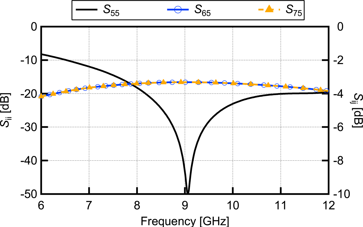
On the other hand, Feed Circuit-2 contains another microstrip-to-slot branch. This branch acts as a 2-way power divider where slot branches on the same slot line form a parallel branch. The output microstrip line of the 3-way power divider is used as an input for the Feed Circuit-2. The microstrip line is extended over slot line with a length of quarter wavelength (λ M/4) at the design frequency and extended microstrip line acts as a short circuit here, so that the total power can be transferred to the slot line. Characteristic impedances of the slot line and microstrip line in the 2-way power divider should maintain a relationship as presented in equation (3) to split half of the input power into each slot branch. Figure 3 illustrates the S-parameters of this branch.
 $$ Z_{\rm S} = 2Z_{\rm MS}. $$
Fig. 3. Simulated S-parameters of the microstrip-slot branch in Feed Circuit-2.
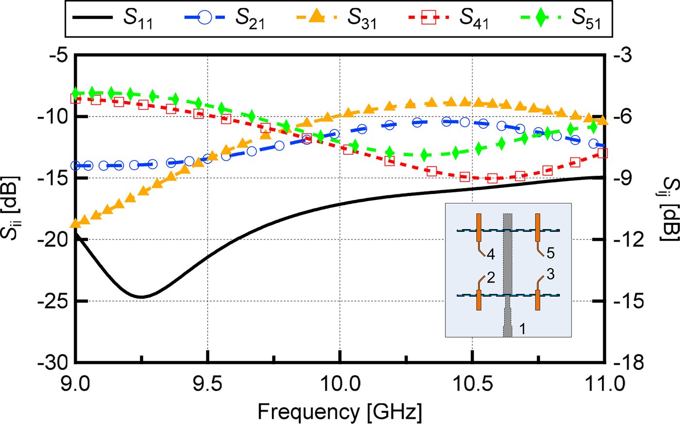
In the feed network, microstrip lines with the width of M MW on both ends of the same slot line are used to feed the patches. Characteristic impedances of the microstrip line and slot line are kept the same. Furthermore, one of the ends of the microstrip line and slot line are extended up to quarter wavelength (λ M/4 and λ S/4) from the branch point. The extended portions of the microstrip line and slot line act as a short circuit and open circuit, respectively. Quarter-wavelength impedance transformers are used between microstrip lines and patches where one of the ends of these transformers at the patch side is at ±45° with respect to the x-axis to ensure the orthogonal feeds for each patch. Figure 4 shows the simulated S-parameters of the complete feed network of the proposed array. It is seen from the figure that one-quarter power (− 6 dB) is received by each feed line of the patches at around 9.85 GHz.

Fig. 4. Simulated S-parameters of the whole feed network. Input port is denoted by 1 and output ports (2-5) are placed at one of the ends of the impedance transformers at the patch side.
It is well known that slot lines cause radiation. But slot lines in conjunction with microstrip lines are used to design the whole feed network as this technique gives easy design. When a slot line and microstrip line cross each other at right angle, it acts as a power divider. Moreover, a tight coupling can be achieved when the width of the microstrip line and slot line are optimally related and they are extended approximately quarter wavelength beyond the point of crossing. Use of a high permittivity substrate can reduce the radiation [Reference Cohn35,Reference Mariani, Heinzman, Agrios and Cohn36] caused by slot lines. The slot-mode wavelength λ′ need to be smaller compared to the free-space wavelength λ 0 to confine the field near the slot for negligible radiation and the relation between them can be demonstrated by the following equation [Reference Cohn35]:
 $$ \lambda^{\prime}/\lambda_ 0 = {\sqrt{2/({\varepsilon_{\rm r}}+1)}}. $$
The condition of λ′/λ 0 < 1 is sufficient to ensure decay of the slot-mode field at the radial distance. Though it should be noted that, the use of high permittivity substrate causes low efficiency and narrow bandwidth [Reference Ittipiboon, Bahl, Bhartia and Garg37]. Therefore, the dielectric permittivity of the substrate should be <2.5 to enhance the fringe fields. While the high permittivity substrate is tried to use in the design, it is required to trade-off between the radiation performance and efficiency. Therefore, in this study, low permittivity substrate has been chosen to design the proposed array antenna.
To get the CP in each patch, two orthogonal modes with quadrature phase shift need to be excited. In the proposed antenna, two orthogonal modes are realized by orthogonal feed technique. Feeds of the Feed Circuit-2 are arranged quarter wavelength ahead from the feeds of Feed Circuit-1 by maintaining the relationship among different lengths presented in equation (5):
 $$ (a + b) - c = n \times {\lambda/4}, $$
where n is an odd number and λ is the wavelength at the design frequency.
Equation (5) ensures the quadrature phase difference between two orthogonal modes in a patch element. Therefore, each of the patch elements is circularly polarized.
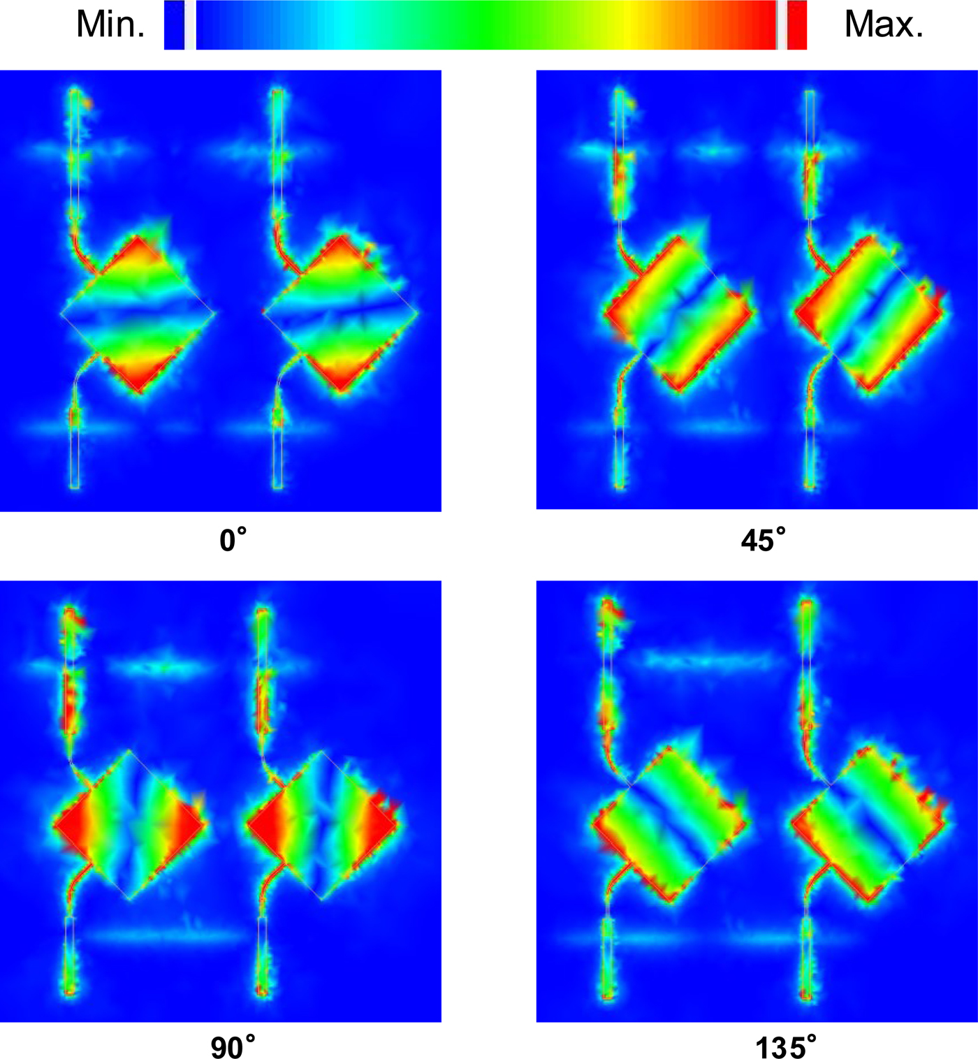
Figure 5 illustrates the electric field distribution of the upper layer of the antenna for different phase instants from 0° to 135° with an interval of 45°. It is clear from the figure that a quadrature phase difference is obtained by using the designed feed network as the field intensity of the same side port of each patch becomes maximum while the other port of the same patch is going to be high after an interval of 90°. Besides, a circularly rotated counterclockwise field with increasing phase is observed. It indicates that a RHCP radiation is achieved.

Fig. 5. Electric field distribution of the multi-layer array antenna for different phase instants from 0° to 135° with an interval of 45°. Counterclockwise rotation is observed.
Benefit and application of the proposed feed structure
The feed network for the proposed array antenna is designed using both-sided MIC technology. Features and applications of the both-sided MIC technology have been studied in detail in [Reference Aikawa and Ogawa33,Reference Egashira, Nishiyama and Aikawa38]. The merit of the proposed feed network is simplicity and easy design process. Conventional array feed networks and their characteristics have been investigated in [Reference Levine, Malamud, Shtrikman and Treves39,Reference Newman and Tehan40]. Generally, corporate feed network [Reference Lu and Chang8,Reference Choi, Pyo and Choi9] and series feed network [Reference Pozar and Schaubert10–Reference Evans and Sambell12] are used for array antennas. In case of corporate feed, due to the longer microstrip feed lines, it suffers gain loss with high sidelobe and cross-polarization level for resistive loss and feed radiation. But the series feed structure is comparatively smaller and more compact than the corporate feed network and moreover, this structure leads to less complex structure, lower spurious radiation, and feedline losses. Practically, the radiation from the series feed network can be significant and it can have a noticeable effect on the array radiation pattern [Reference Shen, Zhou, Huang and Chio41]. The design process is a bit complex for both conventional feed techniques as they require many calculations for step-by-step impedance transformation and need to use impedance transformers for impedance matching.
Figure 6 shows the feed network used in the proposed array. In this feed network, no impedance matching circuits are required for impedance transformation due to the combination of parallel branches and series branches. The impedance relationship of the proposed feed network is as follows: At the 3-way power divider, according to equations (1) and (2)
 $$ Z_2, Z_3 = 100\,\Omega \; {\rm and} \; Z_4 = 50\,\Omega. $$
Slot impedances at the 2-way power divider according to equation (3) is
 $$ Z_5 = 100\, \Omega. $$
As the same power will be transferred from slot lines to microstrip lines at output ports, Port 2, Port 3, Port 4, and Port 5, the impedances of the slot and microstrip lines should be same. Therefore
 $$ Z_7, Z_{10} = Z_3, Z_5. $$
Moreover, the impedances throughout the slot lines and microstrip lines are same and due to the shorted slot stub and open microstrip stub, the electrical lengths of the extended microstrip lines and slot lines are
 $$ \theta _6, \theta _8, \theta _9, \theta _{11}, \theta _{12} = 90^{\circ}. $$
The electrical length of θ 4, θ 7, and θ 10 are determined by the equation (5) where θ 4, θ 7, and θ 10 are equivalent to the physical lengths a, b, and c, respectively. On the other hand, θ 3 and θ 5 depend on the spacing between patches, d M. From the above impedance relationship, it is evident that only 50-Ω and 100-Ω characteristics impedance lines are used to design the whole feed network. This simplicity also makes the feed structure suitable to design extensible array network.
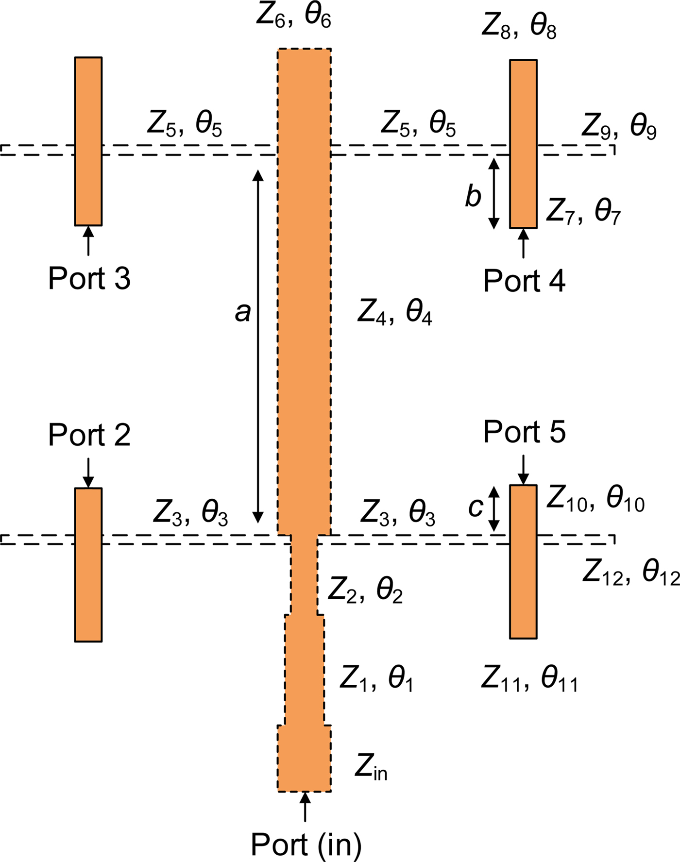
Fig. 6. Model of the feed network for 1 × 2 array structure. Z and θ denote characteristic impedance and electrical length of the transmission lines, respectively.
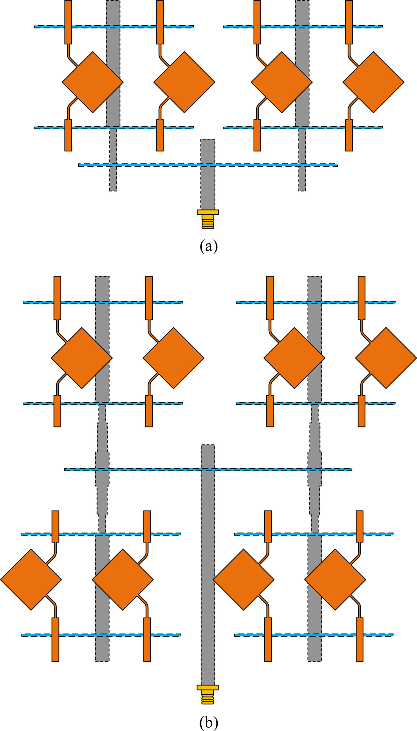
Figure 7 presents an array size extension technique by employing the proposed feed network mechanism. It is seen that the array size can be increased easily by 1 × 4, 2 × 8, 2 × 4, 4 × 8 and so on. In this case, the least number of impedance transformer is required and array size extension is possible by only using 50-Ω and 100-Ω microstrip and slot lines. Therefore, this technique significantly reduces the impedance matching calculation and provides a simple structure with easy design method compared to conventional array feed network techniques.

Fig. 7. Array extension considering the array as shown in Fig. 1 as a unit array. (a) 1-D array (1 × 4). (b) 2-D array (2 × 4).
Parametric analysis
Two main parameters that affect the performance of the antenna are considered here for parametric analysis. One of them is the distance between two slot lines, a, which has a direct effect on the AR performance. The spacing between the patch elements, d M is another parameter to control the sidelobe level. Besides, the effect of width of the slot lines and the thickness of the copper foil are also investigated in this section.
Effect of the distance between two slot lines
Figure 8 shows the effect of “a” on the AR performance. This parameter is very important to ensure good AR by fulfilling the condition as presented in equation (5). To get a good AR performance, the distance between two slot lines should be adjusted properly to create 90° phase difference between two orthogonal feed lines of each patch. To do this analysis, slot line of the Feed Circuit-1 is kept fixed and the slot line of the Feed Circuit-2 is shifted to get the proper phase difference between two orthogonal modes. This means that the value of a and b are increased or decreased by an equal amount while the value of c is fixed. It is found that by increasing the distance between two slot lines, the AR moves to an optimum value. a = 24.24 mm is used for the designed antenna as the optimum distance between slots to get a better AR.
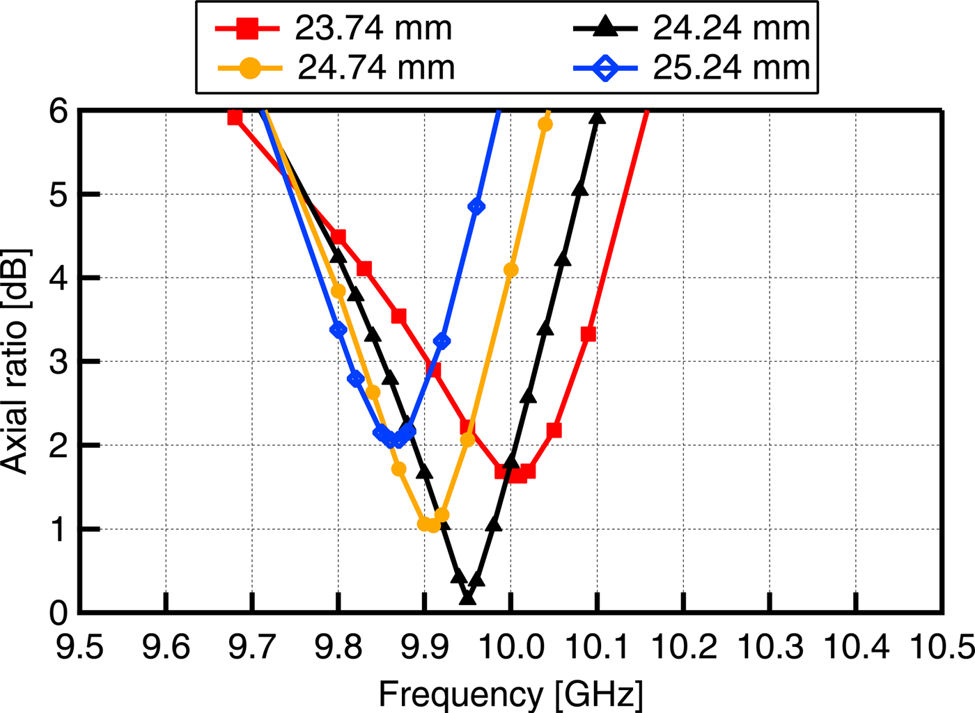
Fig. 8. Effect of “a” on the AR performance.
Effect of the spacing between patch elements
Figure 9 shows the radiation performance of the single layer antenna presented in [Reference Rahman, Nishiyama, Toyoda, Hossain and Hossain34]. From this figure, it is observed that the sidelobes are high and the measured gain is 7.39 dBic. Therefore, it is evident that the high sidelobes reduce the gain of the antenna. It is noticed that the sidelobe level depends on the spacing between the patches. But in the case of single layer structure, when this distance is tried to be optimized for good radiation performance, one of the patches overlaps with the main microstrip feed line. Therefore, to overcome this problem, a multi-layer structure is considered as shown in Fig. 1.

Fig. 9. RHCP radiation performance of the single layer antenna when distance between two patches is 1.22λ 0.
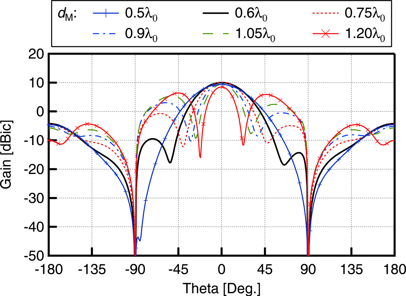
Figure 10 presents the effect of “d M” on the radiation performance of the multi-layer structure. The gain curves are plotted at different frequencies considering the minimum AR value as a little frequency shift occurred for different “d M” values. It is observed that when the distance between the patches increases, the sidelobe level also increases. Therefore, it is possible to get an optimum radiation performance using the multi-layer structure when the distances between the patches, “d M” is 0.6λ 0.

Fig. 10. Effect of “d M” on the RHCP radiation performance of the multi-layer structure. Each curve is plotted at the frequency where the AR becomes minimum.
Effect of the slot width
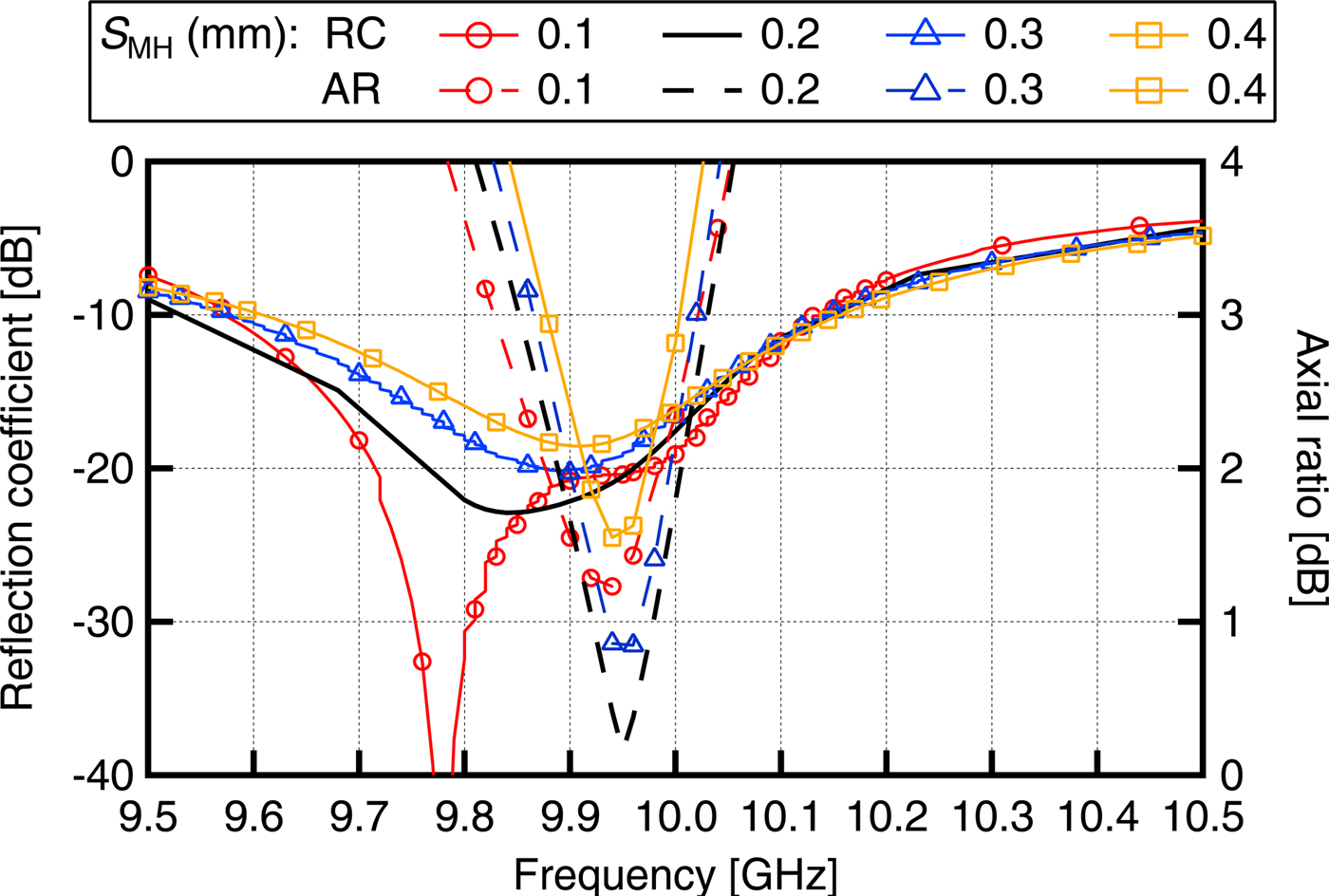
Figure 11 illustrates the effect of “S MH” on the RC and AR performance. It is seen that the optimum AR performance is obtained at the slot width of 0.2 mm (equivalent to 107-Ω) as the proper power division is achieved at the 3-way power divider and the 2-way power divider according to equations (1), (2), and (3). 107-Ω slot lines are used in this structure as 100-Ω slot lines equivalent to 0.14 mm is not possible to fabricate in the authors' laboratory. Although the design and calculation are done considering 100-Ω slot line for simplicity. This inconsistency leads to some performance degradation. In this structure, two 0.2-mm slot lines are used on the back side of the patches and it is well known that slot line causes radiation. So the back radiation of the array is a bit higher than conventional array.

Fig. 11. Effect of the slot width (S MH) on the RC and AR.
Figure 12 shows the front-to-back (F/B) ratio of the antenna. It is observed that the F/B ratio decreases for the wider slot width. It indicates that the back radiation is increased. Therefore, it is better to use narrow slot lines, though the increase of back radiation is not significant as around 0.3 dB is increased or decreased for 0.1 mm slot width variation.
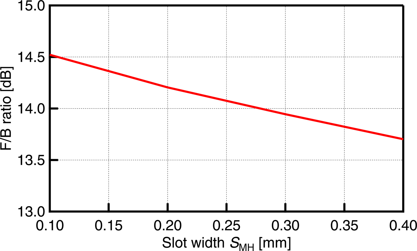
Fig. 12. Front-to-back (F/B) ratio of the array antenna for different slot width.
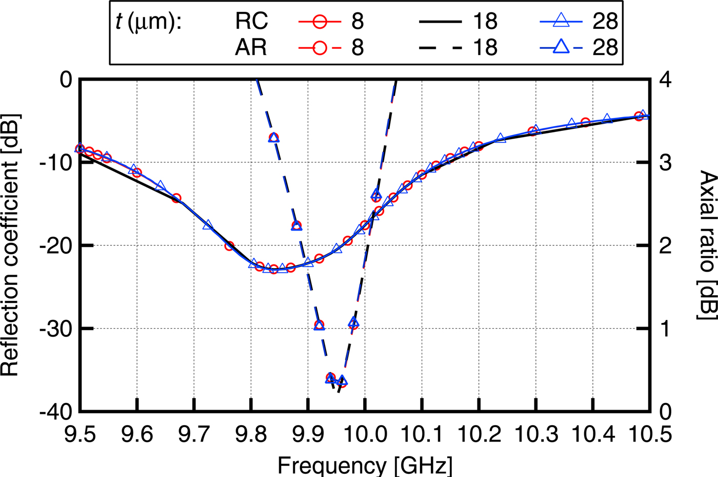
Effect of the thickness of copper foil
Figure 13 shows the effect of the copper foil thickness “t” on the array performance. In the case of microstrip antenna, the thickness of copper foil does not havea significant role on the antenna performance compared to the thickness of the dielectric substrate. Figure 13 also verifies this statement as the RC and AR performances are identical for the variation of the copper foil thickness. 18- $ {\rm \mu} {\rm m}$ thick copper foil layer is used during the simulation of the proposed array antenna as it is available in the authors' laboratory.

Fig. 13. Effect of the thickness of copper foil (t) on the RC and AR of the array antenna.
Antenna performances and discussion
Figure 14 illustrates the photographs of the proposed multi-layer antenna prototype for X-band wherein different layers are presented separately. To fabricate the multi-layer array antenna, Teflon glass fiber substrate (thickness = 0.8 mm, ε r = 2.15) is used for both substrate layers. The overall dimension of the ground plane is 63 mm × 46 mm. Simulation has been carried out by Momentum of Keysight Technologies' Advanced Design System (ADS). Antenna's performances have been measured in an anechoic chamber by using a network analyzer of HP8510C.
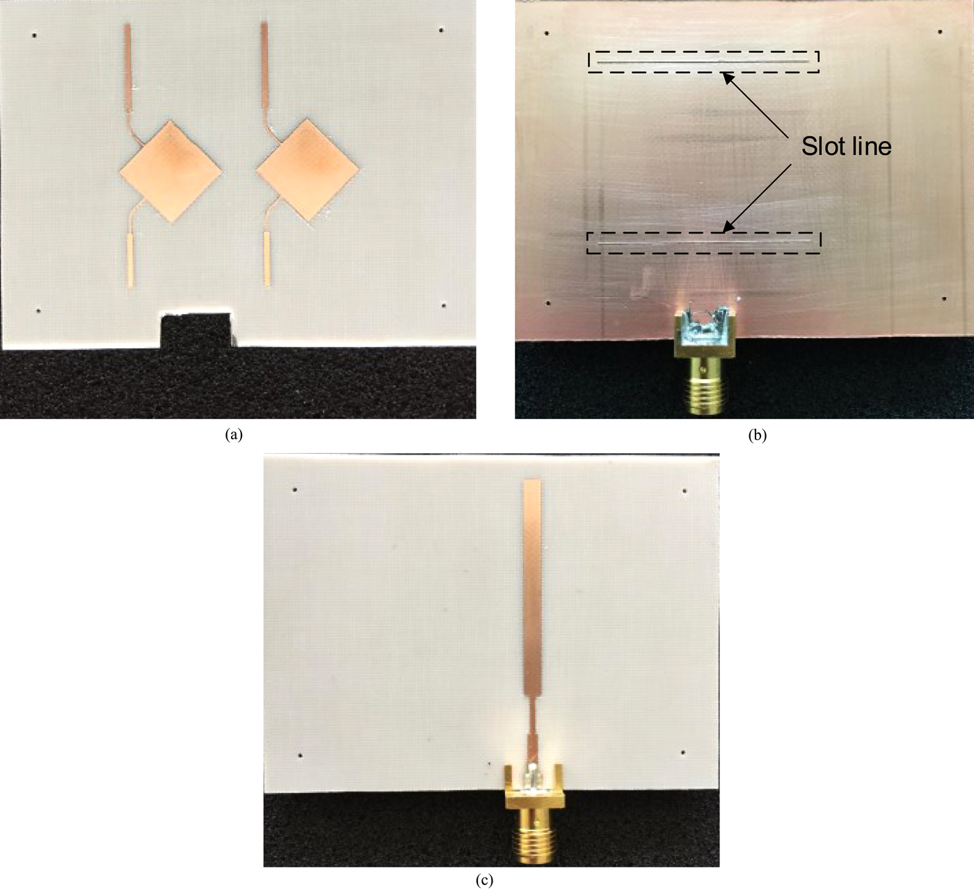
Fig. 14. Prototype of the proposed 10-GHz band multi-layer antenna (63 mm × 46 mm). (a) Top layer. (b) Mid (ground) layer. (c) Bottom layer.
Figure 15 presents the RC of the multi-layer antenna. The measured 10-dB impedance bandwidth of the antenna is 6.1% with a simulated bandwidth of 6.41%.
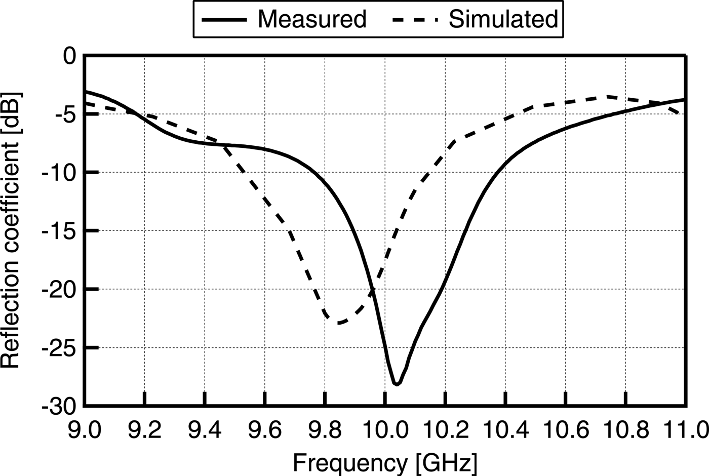
Fig. 15. Measured and simulated RC of the proposed multi-layer orthogonally fed array antenna.
Figure 16 depicts the AR of the antenna. The measured AR bandwidth (<3 dB) is 2.21% from 10.09 to 10.32 GHz while the simulated AR shows a 3-dB bandwidth of 1.86% from 9.85 to 10.04 GHz. Measured minimum AR value is 0.56 dB at 10.22 GHz. The measured 3-dB AR beamwidths in the x–z and y–z planes are 76° and 60°, respectively. A small difference is observed between measured and simulated results. The difference is caused due to fabrication and simulation imperfection. The substrate material is not completely uniform in actual condition. The same thing could also happen when the copper layers are laminated on both sides of the substrate. Whereas the substrate in simulation is considered as uniform material. Moreover, the antenna consists of two separate substrate layers that are not bonded tightly in fabrication as simulation. Another thing needs to be mentioned here is that the simulation is done considering an infinite ground plane. Moreover, the coaxial transition is also not considered in the simulation. So, these are the reasons behind the difference between measured and simulated results.
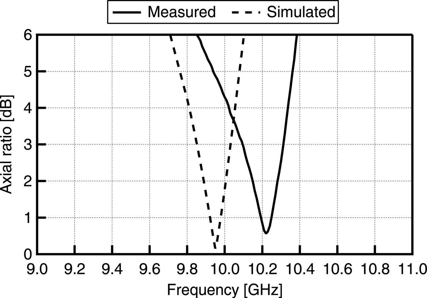
Fig. 16. Measured and simulated AR performance of the proposed multi-layer orthogonally fed antenna.
To get the CP gain of the proposed antenna, the amplitude and phase of the horizontal and vertical field components are measured in an anechoic chamber relative to the signal generator and a double-ridged waveguide horn antenna. The measured real and imaginary components of the horizontal and vertical fields are used for direct conversion from dual linear to RHCP and LHCP power at each measurement angle θ. As a practical CP antenna generates cross-polar power, a correction factor is applied according to [Reference Maci, Gentili and Avitabile1] to compensate the error due to the finite AR caused by an elliptically polarized field pattern.
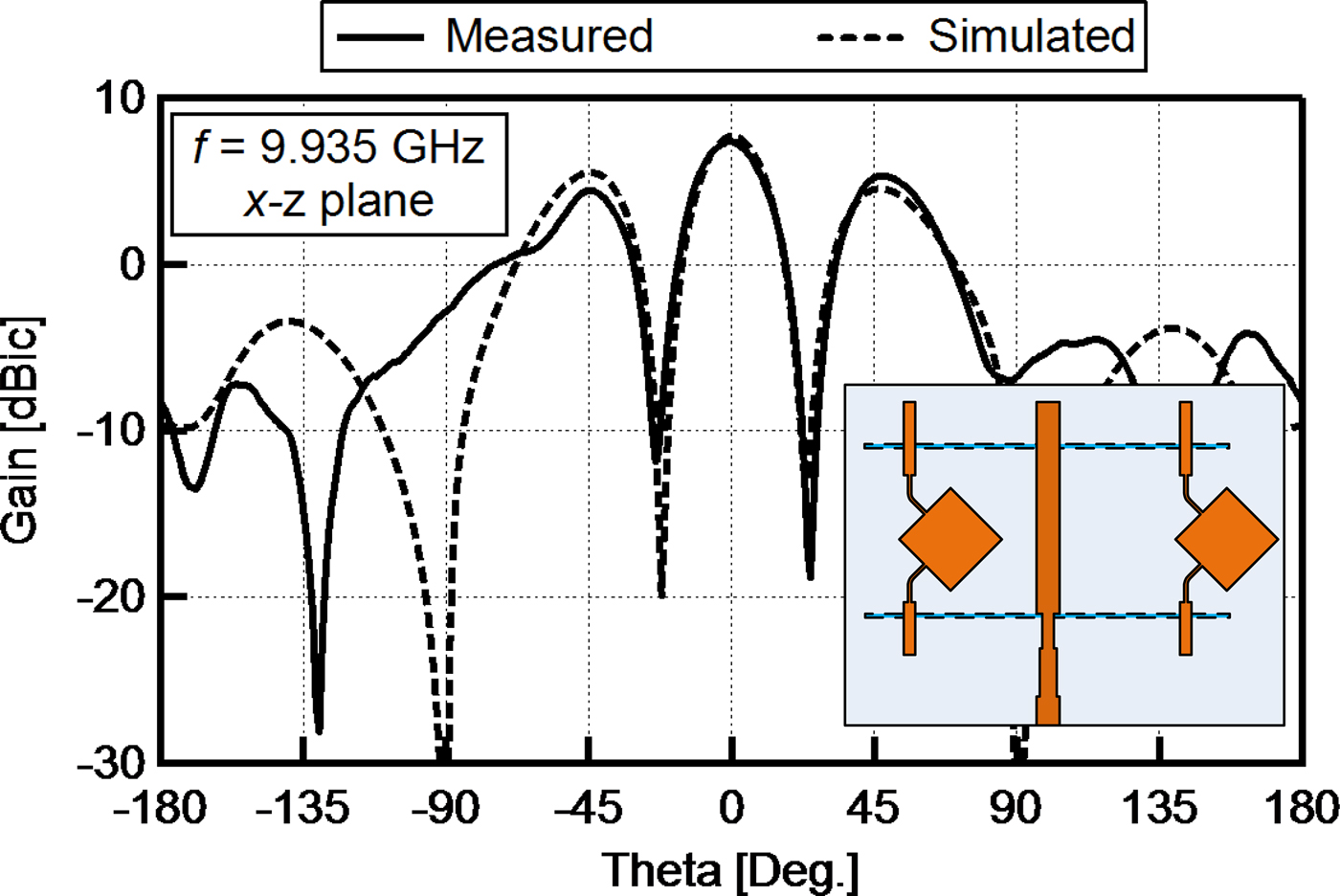
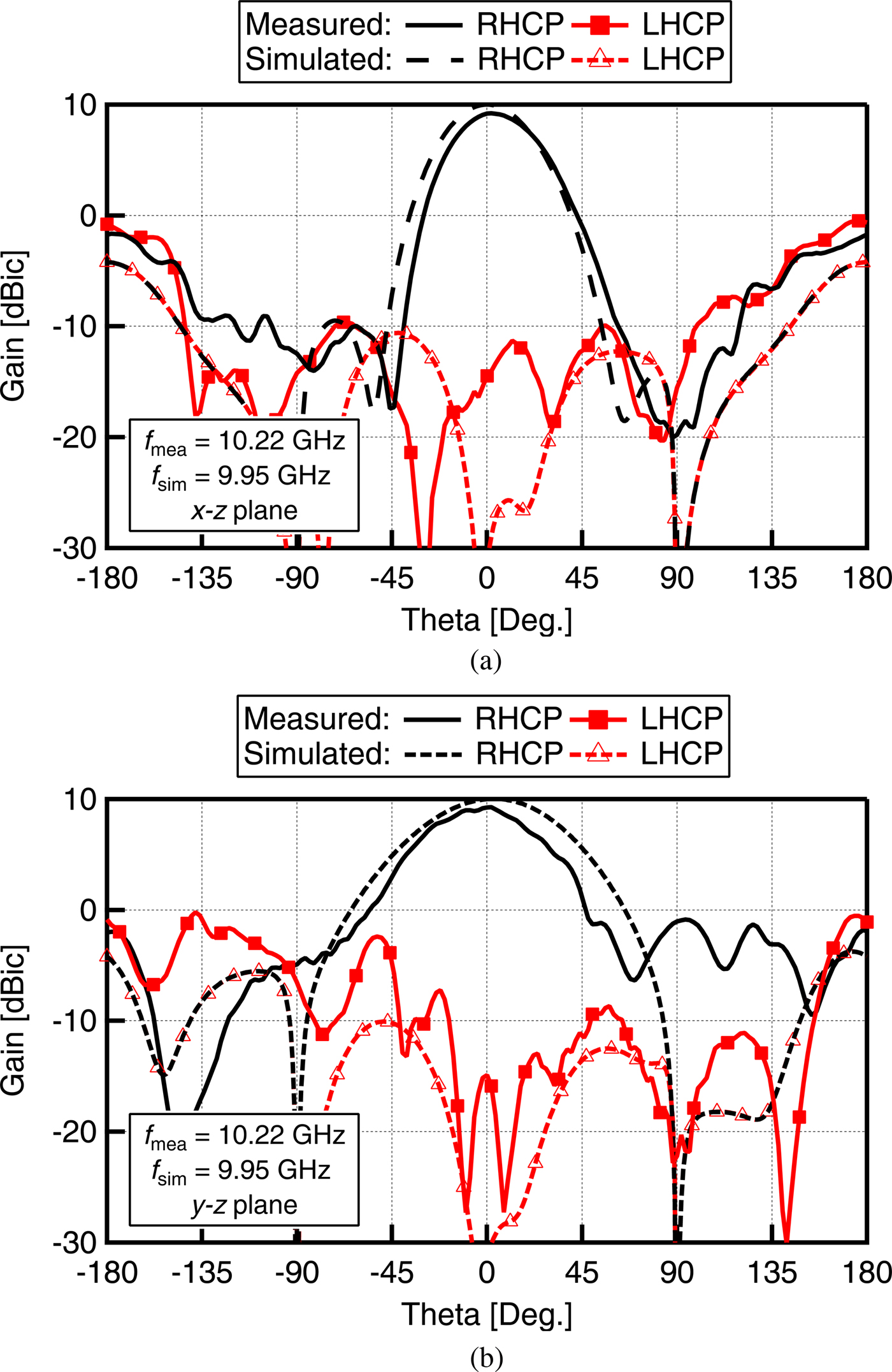
Figure 17 demonstrates the CP performances of the multi-layer antenna in the x–z and y–z planes. Measured and simulated CP radiation patterns are plotted at the frequency where the AR is minimum. It indicates that the radiation of the antenna is RHCP. The measured cross-polarization component of the antenna at both planes are <−23 dB, that ensures a good CP performance of the antenna. Moreover, the measured and simulated performances of the antenna show almost similar characteristics, though a small difference is observed between the measured and simulated radiation patterns from 90° to 135° in Figure 17(b). This difference is caused due to the plot of the measured and simulated patterns in two different frequencies where the measured AR value is above 3-dB level at the frequency of simulated minimum AR and vice-versa. Both show almost similar pattern when they are plotted at 10.22 GHz but at that frequency, the cross-polarization component is very high due to high AR value. Therefore, the comparison between the patterns is plotted at the frequencies of minimum AR. Because of using two slot lines in the feed network, high back radiation is also observed in the patterns of Figure 17. Though the width and length of the slot lines are tried to keep minimum as far as possible during array design as mentioned in the section “Effect of the slot width”. Use of high permittivity dielectric or reflector can be two possible ways to reduce back radiation produced by slot lines. But, both have a shortcoming. High permittivity substrate will reduce the efficiency and bandwidth. On the other hand, the use of the reflector causes the large antenna size. One of these two possible ways should be applied to obtain negligible radiation from slots to use in high profile wireless applications. It seems that the F/B ratio of the presented antenna is withina reasonable limit and not a big concern for low profile applications.

Fig. 17. CP radiation patterns of the multi-layer antenna at the frequency where the AR is minimum. (a) x–z plane. (b) y–z plane.
Figure 17 also confirms that the measured maximum gain at 0° is around 9.25 dBic in the x–z and y–z planes. The gain of the single layer antenna was 7.39 dBic as shown in Figure 9. Therefore, the gain of the multi-layer structure compared to the single layer structure is enhanced by 1.86 dB. On the other hand, it is observed by comparing Figures 9 and 10 that the sidelobe level is reduced significantly in case of the multi-layer approach.
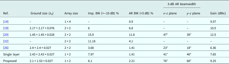
Table 1 presents a comparison among the proposed array antenna and other previously reported CP array antennas. It is seen that the proposed antenna shows a moderate performance. Impedance and AR bandwidths of the proposed antenna are narrower than [Reference Li, Zhang and Feng19,Reference Ding, Gao, Yu, Qu and Zhang20,Reference Lo, Chan and Luk22] because the sequential phase rotation technique that helps to achieve wideband performance is applied to design these antennas. On the other hand, the proposed antenna shows wider bandwidth compared to perturbation type antennas as the CP antennas using perturbation show narrower AR bandwidth (≤1%). Wider 3-dB AR beamwidth is achieved in the proposed antenna due to the dual-feed technique as orthogonal feeds in a patch help to reduce coupling and feed phase deviations. It is evident that similar performances as like as conventional CP array antennas are obtained. On the other hand, the antennas in [Reference Li, Zhang and Feng19,Reference Ding, Gao, Yu, Qu and Zhang20] show wider AR bandwidth, but they are not suitable to form extensible array antenna. The main advantage of the proposed antenna is a simple and easy technique to design the feed network. Comparing with the conventional feed networks such as corporate and series feed networks designed using microstrip lines, the step-by-step impedance matching is not required and impedance matching can be achieved easily by using the feed network of the proposed antenna. Moreover, the performances are not degraded for designing the feed network using a multi-layer approach. The whole feed network is split into three metal layers separated by two dielectric substrates to facilitate the adjustment of the patch spacing. As a result, the enhanced gain with lower sidelobes and compact structure compared to single layer configuration has been obtained. Therefore, the proposed antenna is suitable for the many applications such as portable radar, RFID receiver, mobile ground station for satellite and terrestrial communication, where wideband performance is not necessary.
Table 1. Comparison of the proposed antenna with previously reported antennas.
Conclusion
In this paper, a multi-layer orthogonal feed microstrip array antenna for CP has been demonstrated along with measured and simulated performances. Two patches inclined at 45° with respect to the x-axis and orthogonal feed lines are used to realize the CP array antenna. A new 3-way power divider consisting of microstrip line and slot line is designed and both-sided MIC technology is used to realize the feed network of the array. The proposed antenna layout offers a compact multi-layer structure with high gain compared to a single layer structure. The multi-layer structure provides the flexibility to adjust the distance between patch elements. The proposed antenna structure comparing with a single layer structure gives lower sidelobes that lead to higher gain. Around 2-dB gain improvement indicates the effectiveness of the proposed approach. Good CP performances are also achieved with a 3-dB AR bandwidth of 2.21%. The good radiation performances of the antenna make it attractive for different wireless applications.
Author ORCIDs
Muhammad Asad Rahman, 0000-0002-4749-7953.
Acknowledgments
The authors would like to thank Dr. Takayuki Tanaka, Saga University for his fruitful discussions.
 Muhammad Asad Rahman received his B.Sc. and M.Sc. degrees in Electrical and Electronic Engineering from Chittagong University of Engineering and Technology (CUET), Bangladesh in 2009 and 2014, respectively. He pursued his Ph.D. degree in 2018 from Saga University, Japan. During his Ph.D. study, he was awarded the IEEE AP-S Japan Student of the Year 2017. Currently, he is working as an assistant professor in CUET, Bangladesh. His field of interests are microwave antenna design, reconfigurable antennas, and wireless power transfer. He is a member of IEEE and member of Institute of Engineers, Bangladesh.
 Eisuke Nishiyama received the Doctor Engineering degree from Kyushu University in 2005. He is currently an associate professor with the Faculty of Science and Engineering at Saga University, Japan. He was a visiting scholar with the Electrical Engineering, UCLA (2007–2008). His research interests are in reconfigurable microstrip antennas and rectennas. He served as a vice-chair of the IEEE Antennas and Propagation Society Fukuoka Chapter (2011–2012) and as a chair (2013–2014), respectively.
 Md. Azad Hossain (member, IEEE) is an associate professor in the Chittagong University of Engineering and Technology (CUET), Chittagong, Bangladesh. He received the B.Sc. degree in Electrical and Electronic Engineering from Rajshahi University of Engineering and Technology (RUET), Rajshahi, Bangladesh, in 2004. He was awarded the Master of Engineering degree in EEE from Saga University, Saga, Japan, in 2010; and the Ph.D. degree in Science and advanced Technology, in 2013 from the same Institute. His research interests include Microwave antenna design and related readout circuit simulation and experimental characterization.
 Quazi Delwar Hossain (MIEEE) was born in Barisal, Bangladesh, in 1976. He received the B.Sc. degree in electrical and electronic engineering from Chittagong University of Engineering and Technology (CUET), Chittagong, Bangladesh, in 2001; the Master of Engineering degree in semiconductor electronics and integration sciences from Hiroshima University, Hiroshima, Japan, in 2007; and the Ph.D. Degree in microelectronics from the University of Trento, Trento, Italy, in 2010, working on the design and characterization of a current assisted photo mixing demodulator for time-of-flight based 3-D CMOS image sensors. During his Ph.D. program, he also spent a period with the Smart Optical Sensors and Interfaces Group, Foundation of Bruno Kessler (FBK), Trento, Italy as a Postgraduate Researcher. Presently he is working as a Professor with the Faculty of Electrical and Computer Engineering, CUET. His research interests include VLSI circuits, Microwave circuits and systems, CMOS Based Image Sensor with related readout circuits and Bio-medical electronic systems.
 Ichihiko Toyoda received the B.E., M.E. and Dr. Eng. degrees in communication engineering from Osaka University, Osaka, Japan, in 1985, 1987, and 1990, respectively. From 1990 to 2011, he was engaged in research and development of the 3-D and uniplanar MMICs, ultra-high-speed digital ICs, millimeter-wave high-speed wireless access systems and their applications at NTT Laboratories and NTT Electronics Corporation. He was also active in developing IEEE 802.11, 802.15 and other national standards. He is now a Professor, Vice dean and Advisor to the President at Saga University, Japan. His current interests concern microwave circuit and antenna technology for advanced wireless systems. Dr. Toyoda received many awards from IEICE, international conferences and NTT. He was also recognized as an Excellent Educator by Saga University. He is a senior member of IEICE and a member of IEEE, EuMA and IEEJ.