I. INTRODUCTION
A novel trend in research and design of radar systems is on software-defined architectures. They allow development of waveform-agile radars that can be easily reconfigured to work with different kinds of waveforms without the introduction of any hardware modification. The research done on this topic by the microwave technology and systems for radar (MTSR) group has led to the development of polarimetric agile radar in S- and X-bands (PARSAX) [Reference Krasnov, Babur, Wang, Ligthart and van der Zwan1], a continuous wave Doppler polarimetric weather radar used for atmospheric remote sensing (study of clouds and distribution of precipitation). The PARSAX concept [Reference Krasnov, Ligthart, Li, Lys and van der Zwan2] is meant to transmit and receive two dual-orthogonal signals simultaneously. More precisely, the two transmitted signals are orthogonal both in polarization and in their inner product. This makes possible simultaneous measurement of the complete scattering matrix relative to the area covered by the radar transmission. The software-defined architecture allows the use of different kinds of waveforms, such as linear frequency modulated (LFM), and Phase-shift keying (PSK), depending on the scenario.
An improvement of the PARSAX system could be the extension of the simultaneously scanned area. This could be done by replacing its directive antenna system with an antennas array and introducing proper transmission and reception techniques. The idea is to employ colored space coding techniques [Reference Le Chevalier3] in a multi-channel radar architecture. Orthogonal waveforms are transmitted in different spatial directions, in reception algorithms based on space-time adaptive processing (STAP) [Reference Farina, Fabrizio, Melvin and Timmoneri4, Reference Klemm5] are used to extract the contributions coming from each different direction. Other advantages related to such an idea are a reduction of clutter contributions [Reference De Maio, Fabrizio, Farina, Melvin and Timmoneri6], an enhanced Doppler resolution and estimation [Reference Le Chevalier3, Reference De Maio, Fabrizio, Farina, Melvin and Timmoneri6]. The starting point in such improvement is the development of a multi-channel radar front-end architecture capable of generating and receiving different kinds of waveforms on multiple channels. This radar front-end architecture, which will be referred to as multichannel digital platform, could be used as a testbench to test and validate these transmission and reception techniques. This platform employs an implementation based on direct digital synthesizer (DDS) and field programmable gate array (FPGA) which ensures both system reconfigurability and channels expandability. This allows an “in-field” customization of the radar system's main parameters.
This paper presents a scalable multi-channel digital platform that has been developed to fit such purpose. The designed hardware architecture is described in Section II, then some experimental results are shown in Section III.
II. PLATFORM ARCHITECTURE
The designed multi-channel digital platform (Fig. 1) respects the requirements of expandable number of channels both in transmission and reception, flexible generation and reception of signals and cost-effectiveness. These requirements are principally related to the experimental nature of the platform and are fulfilled with a modular structure implementation, reprogrammability of every platform subsystem and by using commercial off-the-shelf components. The platform is composed of a DDS-based transmitter, an FPGA-based receiver, and a PC that acts as radar back-end. The transmitter generates intermediate frequency (IF) signals on N generic transmission channels. The receiver presents M input channels, whose IF signals are digitized and then processed with proper real-time algorithms implemented on FPGA. Both transmitter and receiver are ready to be connected to the proper radio frequency (RF) front-ends. They are not a part of the designed platform, but have been inserted in Fig. 1 just to highlight how the platform can be employed in a radar hardware structure. Once the platform will be validated, the RF front-ends will be designed and customized according to the chosen antenna system.

Fig. 1. Multi-channel digital platform.
A) DDS-based transmitter
The transmitter architecture (Fig. 2) has been implemented for N = 4. Signal generation is carried out by DDS modules driven by the same reference clock. Each module is an AD9958 evaluation board by Analog Devices which offers two independent output channels with 200 MHz of signal bandwidth. The modules are synchronized through a software synchronization procedure managed by the PC. The controller provides control signals to the DDS boards and the trigger signal to the receiver. It has been implemented using an X3-10M board by innovative integration. This board is based on a Xilinx Spartan 3A DSP FPGA, which ensures controls flexible and fast enough to satisfy DDS maximum performances. A synchronization clock from one of the DDS boards is used as FPGA clock to produce controls synchronized to the DDS boards themselves. A PC is used to set the DDS operational mode (signal type and its specifications) and to reprogram the controller FPGA. Once the operational mode is set, signal generation by the DDS boards is managed by the controller.

Fig. 2. Transmitter architecture.
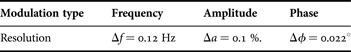
The transmitter output signals are directly generated at IF by 10-bit digital-to-analog converters (DACs) comprised in the DDS boards hardware. The types of supported modulations are frequency, phase, and amplitude with resolutions as shown in Table 1. The device can provide different outputs: single tones, 2/4/8/16-level modulations (such as FSK, ASK, and PSK), and linear sweeps (in all the three modulations).
Table 1. DDS modulations resolution.
The synchronization between DDS boards consists in the alignment between the synchronization clocks. Each clock is used by its own board to sample the controls which act on the output variations. Consequently, any delay between the two clocks results in a corresponding delay between the outputs. A measurement carried out on the two boards at our disposal has shown a synchronization misalignment of 240 ps. This is due to the physical differences between the two devices and can be minimized by acting on the IF output cables phases.
1) FPGA-BASED CONTROLLER
The controller FPGA ensures the capability of generating different types of signals on each channel and precise phase relationships between the channels themselves. In fact, this only involves the development of a proper control logic which, as already said, is clocked on the same timebase of the DDSs. The FPGA logic is implemented in a framework fashion: an “external” framework logic and an “inner” customizable logic (application logic). The external framework, which has been originally designed by the board producer, is realized at VHDL level. It includes all of the interfaces between the application logic and the peripherals available on the board itself (digital I/O port, analog-to-digital converters (ADCs), PCI-e interface, etc.). The application logic is created with Matlab Simulink so it ensures a functional oriented design. In this part of the logic are implemented all the structures that produce proper DDS control signals which will be output through the framework on the FPGA board digital I/O. The Matlab Simulink approach simplifies the realization of different controls required for different signal generations. Once the Simulink design of the application logic is ready, it is converted with the help of Xilinx System Generator in a netlist file that will be merged with the framework logic in Xilinx ISE to obtain the FPGA configuration file.
By default, the FPGA logic, divided in framework and application, is driven by a single clock coming from the PCI-e. In our case, the application logic has to be synchronous to the DDSs, while the framework logic must remain synchronized to the PCI-e to ensure continuous data exchange with the host PC. For this reason the FPGA logic structure has been modified, acting on the framework VHDL top-level and user constraints files, as shown in Fig. 3.

Fig. 3. FPGA logic structure
An additional digital clock manager (a Xilinx logic primitive) has been used to manage the clock coming from the DDS. In such a way, the DDS clock drives the application logic and digital I/O, while the rest of the logic (the framework) is still driven by the PCI-e clock as default. This leads to the presence of two clock domains on the FPGA.
This implementation allows a synchronous control of the DDSs, while maintaining the other on-board peripherals still working correctly. Another important aspect of this solution is related to logic reconfigurability. In fact, simply by acting at a functional level through Matlab Simulink, it is possible to produce different control sets without writing a single line of VHDL. In the case when DDS board numbers has to be increased it is just a matter of adding other parallel control channels inside the application logic exploiting the parallel computing features of the FPGA.
B) FPGA-based receiver
A reconfigurable digital receiver based on FPGA has been already implemented for PARSAX system [Reference Wang, Krasnov, Babur, Ligthart and van der Zwan7]. Following this trend we have chosen the same system implementation for the platform receiver. This makes it possible to test the platform using PARSAX IF waveforms specifications and receiving algorithms. Moreover, the receiver has a bandwidth of 200 MHz matching the DDS-based transmitter one. In this way, the platform can benefit from a versatile receiver capable of treating different kinds of waveforms simply by changing its FPGA logic configuration. The receiver (Fig. 4) is composed of a PC and a X5-400M board by innovative integration which is an acquisition node based on ADCs and on a Xilinx Virtex 5 FPGA.
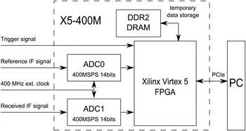
Fig. 4. Receiver block scheme.
This architecture presents M = 2 input channels for the reference and received IF signals. The first is an IF transmitted waveform coming from the transmitter, the second is the received radar signal down-converted at IF. These two signals are digitized by ADCs and acquired by the FPGA according to the trigger signal timing. The two digitized signals are then cross-correlated inside the FPGA with a proper real-time digital signal processing algorithm. The resulting data sets are sent to a host PC, further processed and visualized in a targets range profile. Two algorithms have been already implemented and tested: the de-ramping [Reference Wang, Krasnov, Babur, Ligthart and van der Zwan7, Reference Wang, Krasnov, Ligthart and van der Zwan8] and the matched filtering [Reference Wang, Krasnov, Babur, Ligthart and van der Zwan7]. The first one is suitable for receiving LFM signals, the second is a canonic coherent receiver and is used in PARSAX for receiving PSK signals.
The use of the FPGA allows reception algorithms interchangeability. Since the algorithms implementation on the FPGA is real-time oriented the receiver is also capable of processing and visualizing real-time radar data. The number of receiving channels can be easily increased by simply parallelizing more X5 devices.
III. EXPERIMENTAL MEASUREMENTS
Since we are not dealing with the radar RF parts, the platform correct behavior is checked through a targets simulation configuration (Fig. 5) directly working at IF. This configuration is good for providing a feedback on the correct functionality of the system excluding the RF part impairments. The routing block is simply composed of a manual switch and a summator. The transmitter provides two waveform-orthogonal transmitted signals (Transmitted H and Transmitted V) and two delayed signals (Reflected 1 and Reflected 2). The transmitted waveforms are indicated with H and V to maintain an analogy with the PARSAX system where, due to the dual orthogonality, they are also associated with horizontal and vertical electromagnetic (EM) polarizations, respectively. The delayed waveforms resemble reflections from two different ideal targets (i.e. perfect reflection), each one associated with one of the two orthogonal transmitted waveforms. For this reason, we can interpret the two simulated targets as though they were orthogonal in terms of EM behavior being one reflecting only the H polarization, while the other reflecting the V. The delays needed to simulate target reflections are inserted in the controller FPGA logic. The sum of the delayed waveforms is a model of a signal received by a polarimetric radar and is used as received IF signal. The receiver must discriminate between the two targets according to the reference used (Transmitted H, or Transmitted V). The platform setup can vary according to the used waveform type (LFM, binary PSK (B-PSK), or pulsed waveform), the targets configuration (distance, orthogonality), the receiving algorithm (de-ramping or matched filtering). Some experimental measurements have been performed on a prototype of the platform with three different setups.

Fig. 5. Platform in targets simulation configuration.
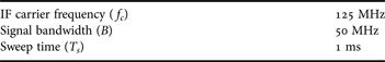
A) Simulation of two orthogonal targets using LFM signals
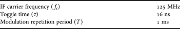
This simulation models the reflections from two orthogonal targets (e.g. at 8 and 12 km) using LFM waveforms. The two transmitted signals are, as in PARSAX, two LFM signals with specifications as in Table 2, one with a linear sweep up trend and the other with a linear sweep down trend. They result to be orthogonal in terms of cross-correlation [Reference Babur9]. The two transmitted waveforms and the relative delayed versions have been generated with the transmitter implementation already explained. The control signals needed to generate this waveforms set are provided by the controller FPGA which has a time base of 16 ns given by the application logic clock period. For this reason, all the delays are multiples of this time base. This also means that the minimum delay which a simulated target can assume is 16 ns. That gives a simulated target range resolution of
 $$\Delta R_{sim} = \displaystyle{{c \cdot 16\;ns} \over 2} = 2.4{\rm\;m}.$$
This value is lower than the de-ramping algorithm range resolution ΔR D = 3.3m [Reference Wang, Krasnov, Ligthart and van der Zwan8] thus the targets simulation capability does not limit the overall platform resolution performance.
Table 2. LFM signals specifications.

The measured signals spectrograms are shown in Fig. 6. The two reflected signals present respectively the delays τR1 = 53.3µs And τR2 = 80µs, given by the chosen targets distances. The spectrogram profiles, obtained by a sequence of short FFTs on a small set of local samples, show a dynamic between the sweep and the spurious frequencies of approximately 60 dB, being the sweep at −30 dB. The sweep amplitude measurement in dB has been verified by directly measuring the amplitude in mV with an oscilloscope and considering the ADC full-scale range. Instead, for an exact spurious frequencies level estimation, further and more precise measurements are necessary. However, this 60 dB is comparable to the −56 dBc of DDS spurious-free dynamic range (SFDR) in the bandwidth 100–150 MHz (as in the AD9958 datasheet), although our measurement is performed in this frequencies range instead of using the DC to Nyquist one. The spectrogram associated with the Transmitted V and Reflected 2 signals shows some artifacts that are related to a worse performance of one channel on one of the DDS boards at our disposal. This is probably related to a lower quality of its 200 MHz passive output low pass filter (implemented with discrete surface mount device (SMD) components) or to some non-linearity introduced by a defect in the DDS IC.

Fig. 6. LFM signals measured spectrograms.
Using the de-ramping processing in reception, the range profiles with reference H or V are obtained (Fig. 7). In both profiles the desired target is correctly detected at a distance that matches the one set in the controller. The dynamic is approximately 80 dB, achieved due to the pulse compression done by the receiver. This process allows a signal-to-noise ratio (SNR) gain over the received signal SNR known as a bandwidth-time (BT) product, in this case 47 dB. The small peak represents instead the orthogonal target which is not completely rejected. Since the de-ramping algorithm implements the cross-channel interferences suppression [Reference Krasnov, Babur, Wang, Ligthart and van der Zwan1, Reference Babur9], the onset of this contribution depends on the reference signal. In fact, the coupling between the two references causes each real reference to also contain an attenuated version of the orthogonal one. In this way, de-ramping is done for both components at the same time, thus leading to the presence of two peaks.

Fig. 7. Two orthogonal targets range profiles using LFM signals.
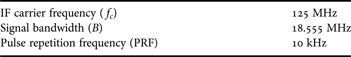
B) Simulation of two orthogonal targets using B-PSK signals
This simulation models two orthogonal targets (e.g. at 2 and 4 km) using B-PSK waveforms (Fig. 8) with specifications as in Table 3. Two orthogonal B-PSK signals are two signals modulated in phase with orthogonal binary sequences. In this case, for simplicity two random sequences have been chosen. To check their orthogonality, a simulation of the matched filtering processing has been carried out. It calculates the four cross-correlations given from the combinations between each reference sequence and each target sequence (obtained simply by circular shifting the relative reference one). The cross-correlation results are used to plot the four simulated range profiles (Fig. 9). When a reference is cross-correlated with its relative target, a peak at the predefined distance is present. When a reference and the orthogonal target are considered, no correlation peak is noticeable. Thus, it is possible to assume the two reference sequences as orthogonal and use them for signals generation.

Fig. 8. B-PSK signal.

Fig. 9. Cross-correlation simulation between orthogonal sequences.
Table 3. B-PSK signals specifications

The matched filtering algorithm, fit to process signals with a −3 dB bandwidth B = 50 MHz, has been modified to allow the whole B-PSK signal bandwidth B = 62.5 MHz to pass. The range profiles in Fig. 10 show correct targets detections, matching simulated ones distances. The dynamic in this case is only 15 dB, so much less than when using LFM waveforms and de-ramping processing technique. This is due a 10 dB lower BT product and a received signal SNR reduction. The lower BT product is related to the fact that matched filtering real-time processing has got a higher computational cost with respect to de-ramping, thus this requires a reduction of the number of acquired samples to maintain the real-time constraint. The lower received signal SNR is due to spectral distortions and aliasing noticed in the measured spectrum (not shown here) and to the intrinsic spread spectrum nature of PSK signals. For these reasons, the orthogonal target is invisible, completely sunk into the noise floor.

Fig. 10. Two orthogonal targets range profiles using B-PSK signals.
C) Simulation of one target using pulsed signal
A pulsed waveform can be obtained with the transmitter using the amplitude modulation mode on a single tone output of frequency f c which acts as a carrier. The receiving algorithm is the matched filtering. A single target (e.g. at 5 km) has been simulated with a delayed version of the pulsed waveform with the specifications as in Table 4.
Table 4. Pulsed signal specifications

A discrete Hamming function with five coefficients has been used to optimize the trade-off between frequency roll-off of the transmitted signal and reception bandwidth. In our case we want to limit the bandwidth inside the 50 MHz bandwidth of matched filtering receiving algorithm but we also want to preserve it quite large still improving the roll-off. That is why the number of coefficients is so small. This ensures a better roll-off with respect to a simple on–off modulation (rect windowing) but still a bandwidth which allows a range resolution of
 $$\Delta R = \displaystyle{c \over {2B}} = 8.08{\rm \;m}.$$
A measurement of the pulse carried out with the oscilloscope can be seen in Fig. 11.

Fig. 11. Pulsed waveform time profile.
The obtained range profile is the one in Fig. 12. The detected target distance matches the set one proving that the generated pulsed waveforms can be correctly received with the matched filtering. The target peak is wider than in previous cases with approximately a −3 dB width of 5.1 m due to lower waveform resolution. Despite the lower resolution, caused by the narrower signal bandwidth, a better dynamic with respect to the B-PSK measurements can be noticed. This is probably due to the fact that narrower bandwidth and higher roll-off of the pulsed waveform spectrum provide less aliasing contributions in reception signal processing.

Fig. 12. One target range profile using pulsed signal.
IV. CONCLUSIONS
The multi-channel digital platform, already tested and validated, fulfills the design requirements: expandable number of channels, waveform-agility, and cost-effectiveness. The library of waveforms for radar applications comprises LFM, stepped frequency, B-PSK, pulsed signals, and the available receiving algorithms are de-ramping and matched filtering. A great advantage of the platform is that it preserves its functionalities even if some subsystems are changed in the model (e.g. different FPGA-based receiver, controller, DDS board, etc.). On the other hand, the platform's main limitation is that it provides only an ideal simulation of a radar, since it works at IF totally excluding radar RF part. Thus, important factors like real transmission channel behavior (e.g. clutter, other types of noise) and RF parts non-idealities are not taken into account. Further developments are principally related to the DDS board, the main one is to characterize the output channels signal quality in terms of noise, SNR, and SFDR. In fact, this measurement would allow us to evaluate transmitter performances and analyze how much the dynamic range in reception is influenced by the DDS SFDR. The other developments on DDS are a proper trimming of the output cables in order to reach the exact synchronization between channels, the adoption of de-emphasis techniques and EMC countermeasures to minimize distortions and coupling. Another improvement, linked to the platform hardware structure optimization, is to use the same FPGA both as digital signal processing core and as platform controller.
The platform can be employed in a real radar system, but before doing that further measurements for evaluating its performance in terms of transmitted waveforms characterization and reception resolution are needed. Right now the platform aims to be a radar hardware test-bench, thus, once the number of channels has been increased, it can be used for evaluating in hardware the transmission and reception of different waveforms combinations, supporting radar research on software-defined multi-channel architectures.
ACKNOWLEDGEMENTS
The work is based on an MSc project carried out by the first two authors at the MTSR group. The authors would like to acknowledge Mr Fred van der Zwan for his technical advice and support to this research and Dr Galina Babur for useful discussions and suggestions, both of them from the MTSR group.
 Giacomo Calabrese was born in Italy in 1986. He obtained the Bachelor's and Master's degree in Electronic Engineering from the University of Florence, Italy respectively in 2009 and 2011. Before the Master's degree, he carried out an MSc program at the TU Delft–MTSR group in cooperation with the University of Florence. He is currently an Information Engineering PhD student at the University of Siena. His research activity, done in cooperation with Texas Instruments – Kilby Europe Labs and the University of Florence, is focused on the study and design of high power density electronic converters.
 Lorenzo Pagli was born in Italy in 1986. He received the Bachelor's and Master's degree in Electronic Engineering from the University of Florence, Italy, respectively, in 2009 and 2011. Before his Master's degree, he was a visitor student in an MSc program held at the TU Delft – MTSR group, in cooperation with the University of Florence. He is actually working as electronic design engineer in a private company based in Florence, specialized in the development of custom electronic solutions. His working activity is mainly focused on board hardware-level design and FPGA development.
 Oleg A. Krasnov received the M.S. degree in radio physics from Voronezh State University, Russia, in 1982, and the Ph.D. degree from National Aerospace University “Kharkov Aviation Institute”, Ukraine, in 1994. In 1999, Dr Krasnov joined the International Research Center for Telecommunications and Radar (IRCTR), TU Delft. Since 2009, he has been a senior researcher at Microwave Technology and Systems for Radar (MTS-R) section of the Faculty of Electrical Engineering, Mathematics, and Computer Science (EEMCS) at Delft University of Technology. His research interests include radar waveforms, signal and data processing algorithms for polarimetric radars and distributed radar systems, and multi-sensor atmospheric remote sensing.
 Alexander G. Yarovoy graduated from Kharkov State University, Ukraine, in 1984 with Diploma with honors in radiophysics and electronics. He received the Candidate Phys. & Math. Sci. and Doctor Phys. & Math. Sci. degrees in radiophysics in 1987 and 1994, respectively. In 1987, he joined the Department of Radiophysics at Kharkov State University as a Researcher and became a Professor there in 1997. From September 1994 through 1996, he was with Technical University of Ilmenau, Germany as a Visiting Researcher. Since 1999, he has been with the International Research Centre for Telecommunications-Transmission and Radar (IRCTR) at Delft University of Technology, the Netherlands. Since 2009 he has led there chair of Microwave Technology and Systems for Radar. In August 2010, he was appointed as scientific director of IRCTR. His main research interests are in ultra-wideband microwave technology and its applications (in particular, radars) and applied electromagnetics (in particular, UWB antennas). He has authored and co-authored some 250 scientific or technical papers, four patents and fourteen book chapters. He served as a Guest Editor of five special issues of IEEE Transactions and other journals. Prof. Yarovoy is the recipient of a 1996 International Union of Radio Science (URSI) “Young Scientists Award” and the European Microwave Week Radar Award in 2001 for the paper that best advances the state-of-the-art in radar technology (together with L.P. Ligthart and P. van Genderen). In 2010, together with D. Caratelli Prof. Yarovoy received the best paper award of the Applied Computational Electromagnetic Society (ACES). Prof. Yarovoy served as the Chair and TPC chair of the 5th European Radar Conference (EuRAD'08), Amsterdam, the Netherlands, Delft, as well as the Secretary of the 1st European Radar Conference (EuRAD'04), Amsterdam, the Netherlands. Prof. Yarovoy served also as the co-chair and TPC chair of the Xth International Conference on GPR (GPR2004) in Delft, the Netherlands. In 2008, he was elected a member of the Board of Directors of the European Microwave Association (EuMA).