I. INTRODUCTION
The main function of an antenna is to radiate radio frequency energy developed in the transmitter and to act as an impedance matching device for matching the impedance of transmission line with the impedance of space [Reference Balanis1]. The low profile, light weight and low cost of manufacturing of microstrip patch antennas made them attractive for many applications. The modern trends in communication systems require wide bandwidth, small-size, and low-profile antennas [Reference Kumari and Gupta2]. In the last decade, the rapid growth in wireless communication technology has led to development of various wireless-communication standards such as WLAN, WiMAX, UMTS, etc. requiring different frequency bands of operation [Reference Parkash and Khanna3–Reference Augustin, Bybi, Sarin, Mohanan, Aanandan and Vasudevan4]. The WLAN and WiMAX applications, covering the bands of 2.4/5.2/5.8 and 2.3/2.5/3.5/5.5 GHz, have stimulated much interest in the research of antennas with multiple bands or broadband [Reference Balanis1–Reference Ghoname, Mohamed and Hennawy14]. For these modern communication systems, antenna with reduced size, wide bandwidth, and multiband operation are becoming important design considerations for practical applications. The various size reduction and broad banding techniques using shorted pins or shaped slots [Reference Augustin, Bybi, Sarin, Mohanan, Aanandan and Vasudevan4], post-gap [Reference Guha and Siddiqui6], or parasitic elements [Reference Iqbal, Siddiqui and Guha7] came in existence, but all these have some disadvantages such as poor efficiency, low gains, low bandwidth, and high cross-polarization. Microstrip antenna with defected ground structure (DGS) can support multiband that can operate at different frequencies and with small size also [Reference Rahardjo, Zulkifli and Marlena8, Reference Saad, Khaled and Salem9]. DGS is realized by etching defects on the ground plane of microstrip antenna, thereby perturbing the shield current distributions in the ground plane, which influences the input impedance and current flow of the antenna. In this DGS technique, the ground plane metal of a microstrip (or stripline or coplanar waveguide (CPW)) circuit is intentionally modified to enhance the performance of antenna [Reference Sharma, Kandwal and Khah13]. The advantage of the proposed antenna has a more compact size as compared with the antennas reported in [Reference Saad, Khaled and Salem9, Reference Arya, Patnaik and Kartikeyan12–Reference Ghoname, Mohamed and Hennawy14]. In [Reference Saad, Khaled and Salem9], the wideband slotted planar antenna occupies a large volume of 50.95 × 59.00 × 1.575 mm3 as compared with proposed antenna design. The second advantage of the proposed antenna has large impedance bandwidth as compared with antennas reported in [Reference Augustin, Bybi, Sarin, Mohanan, Aanandan and Vasudevan4, Reference Zhang, Zhang, Ma, Chen and Zhang10–Reference Ghoname, Mohamed and Hennawy14].
In this paper, the defects are created in ground plane of CPW feed to enhance the bandwidth and reduce the size of antenna. The four vertical monopole-based antennas with CPW-feed having “I” shaped DGS has been proposed to achieve multiband operation covering WLAN and WiMAX bands. The four vertical arms are used to obtain the lower frequency bands. To reduce the antenna size, I-shaped defects are introduced on both sides of ground plane. The slots created in the ground plane, control the flow of current on the antenna surface. The slot dimensions are optimized to improve the antenna parameters such as return loss and antenna size across the targeted frequency bands. The parametric studies are performed to understand the characteristics of the proposed antenna.
II. ANTENNA GEOMETRY
The geometry of the proposed multiband antenna for WLAN/WiMAX applications with DGS-based CPW feed is depicted in Fig. 1. The proposed antenna has a single-layer metallic structure on one side of the FR4 substrate layer, whereas the other side is without any metallization. The fabrication of the proposed antenna is done using a conventional FR4 substrate, with thickness (h) of 1.6 mm and relative permittivity of €r = 4.4, which makes it easy and economical to manufacture. A CPW feed, which consists of a signal strip of width W f of 4.95 mm and two equal finite coplanar ground planes of length L g, width W g and a gap distance of “d” between the signal strip and ground plane of 0.6 mm, is used for feeding the antenna. A conventional CPW on a substrate consists of a center signal strip conductor and two semi-infinite ground planes on either side of the strip and it is proposed by Wen [Reference Wen15]. CPW waveguide structure has been studied by using quasi-static approximation and full-wave analyses. CPW has several advantages over the conventional microstrip line such as lower radiation leakage and less dispersion, wider bandwidth, better impedance matching, simplest structure, light weight, and no soldering point. CPW feed lines also facilitate parallel as well as series connection of both active and passive components on one side of the planar substrate thereby eliminating via hole connections.

Fig. 1. Multiband antenna geometry using DGS technique.
In the proposed design, I-shaped defects are inserted to both the sides of the symmetrically placed ground planes of patch antenna generating a defected ground structure. On the left side of the ground plane, vertical I-shape (L g1) defect is inserted and on the right side of the ground plane, horizontal I-shape (W g2) defect is inserted, which is used to achieve size reduction and better impedance matching.
The basic structure of antenna is a T-shaped monopole with “I”-shaped slots inserted into both the sides of the ground planes, which is responsible for upper frequency band of the proposed antenna. On top of the T-shape structure four vertical arms are placed in such manner to achieve the lower frequency band. Each vertical arm consists of small brick of length L 1 and width W 1 are joined together in such a way that the electrical current length is increased and size reduction is obtained. The horizontal strips joining the four vertical arms are used to merge the different frequency bands, so that wide band operation in lower frequency band and upper frequency band can be obtained. The antenna performance is analyzed by using method of moment-based Zeland IE3D simulator.
The proposed antenna structure has dimensions of length L of 30.54 mm and width W of 24.95 mm. The eight horizontal connecting strips L 2 to L 9 are used with different dimensions length as mentioned in the table. The optimized geometric parameters of the proposed antenna are given in Table 1. Total volume of the proposed antenna is 2 cm3 with overall size of 45.19 × 28.76 × 1.6 mm3. Photograph of the fabricated prototype has been shown in Fig. 2.
Fig. 2. Prototype of the proposed antenna.
Table 1. Optimized parameters of the proposed antenna.

III. SIMULATION AND EXPERIMENTAL RESULTS AND DISCUSSIONS
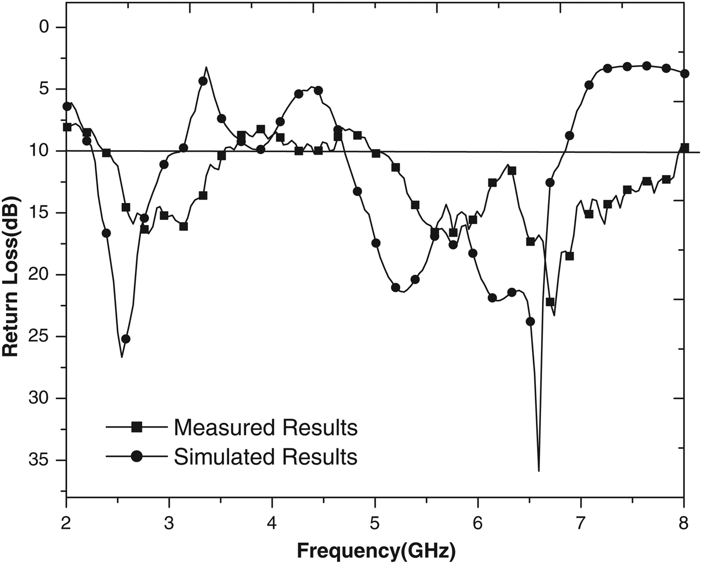
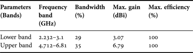
The simulated parametric study and measured results for the proposed monopole antenna have also been observed. The measured and simulated results of return loss are presented for the optimized set of antenna parameters in Fig. 3. From simulated result, it is found that the antenna has multiple resonant frequencies with wide bandwidth. The 10 dB impedance bandwidth of lower band is 29%, ranging from 2.232 to 3.1 GHz, with respect to the central frequency of 2.52 GHz and the bandwidth of the upper frequency band is 2.1 GHz (4.712–6.81 GHz), or about 35%, with respect to the central frequency of 5.7 GHz. Obviously, the proposed antenna has a broader bandwidth covering the required bands of the IEEE 802.11 WLAN standards in the bands at 2.4 GHz (2.4–2.48 GHz), 5.2 GHz (5.150–5.350 GHz), and 5.8 GHz (5.725–5.825 GHz), WiMAX standard in the bands at 2.3 GHz (2.3 –2.4 GHz), 2.5 GHz (2.5–2.690 GHz), small part of 3.5 GHz (3.4–3.69 GHz), and 5.5 GHz (5.250–5.850 GHz). The proposed antenna is fabricated on a substrate using simple screen printing and chemical etching process. The measurement is carried out by using Agilent N8205F vector network analyzer. The measured outcome explores good dual-band operation with 10 dB impedance bandwidths ranging from 2.39 to 3.51 GHz at lower frequency band and from 4.98 to 7.94 GHz at upper frequency band, respectively, and shows good conformity with the simulated results as shown in Fig. 3. The agreement seemed good, and a similar curve trends between the measured and the simulated results are seen over the whole operating band. There is a slight shift of peak resonant frequency toward higher frequency and this discrepancy is due to the slight dimensional errors in the fabrication process and also because of the effect of the cable connector in addition to errors in processing. The effect of connector is not accounted for in the simulation but it was used in the experiment acting as load of a variable reactance.
Fig. 3. Comparisons of simulated and measured return loss.
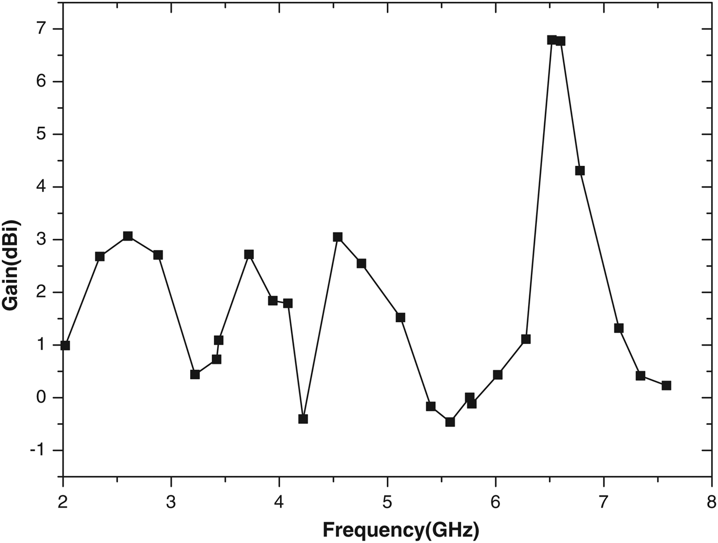
The simulated gain of the proposed antenna is depicted in Fig. 4. The antenna has a maximum gain of about 3.07 dBi at 2.6 GHz in lower frequency band, whereas in the higher frequency band, the maximum antenna gain is about 6.79 dBi at 6.5 GHz. The summary of results of the proposed antenna is given in Table 2.
Fig. 4. Simulated gain of the proposed antenna.
Table 2. Summary of the results of the proposed antenna.
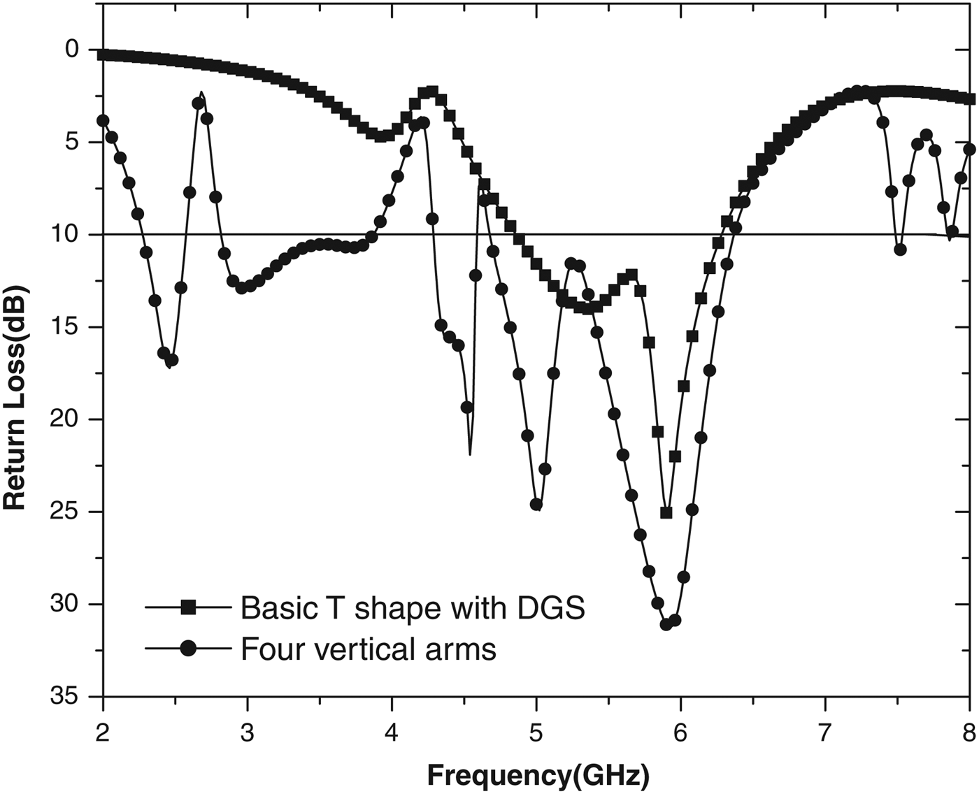
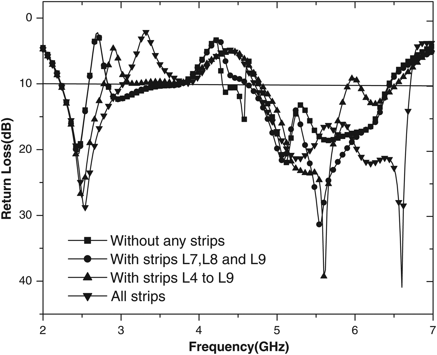
Effect of introducing four vertical arms on antenna performance is presented in Fig. 5. It can be examined from the graph that without the vertical arms, antenna works only at higher frequency band but after including the vertical arms, desired lower frequency bands are obtained, which are further moved closer to each other with the help of horizontal connecting strips to obtain wideband operation. Effects of introducing horizontal shorting strips on proposed antenna return loss with respect to frequency is represented in Fig. 6. It can be seen from the figure that without any horizontal strip in the structure there are four separate frequency bands. After including strips L 7, L 8, and L 9 the band at frequency 4.5 GHz is merged with band at 5.9 GHz resulted in a complete wideband operation from 4.63 to 6.44 GHz. Furthermore on including strips L 4, L 5, and L 6, lower frequency bandwidth is increased but upper frequency wideband is split into two bands. Strips L 2 and L 3 are used to improve the lower frequency band and two upper frequency bands are merged together and resulted in improved impedance bandwidth of 29% in lower frequency band and 35% impedance bandwidth in upper frequency band.
Fig. 5. Effects of four vertical arms on impedance bandwidth.
Fig. 6. Effects of horizontal strips on impedance bandwidth.
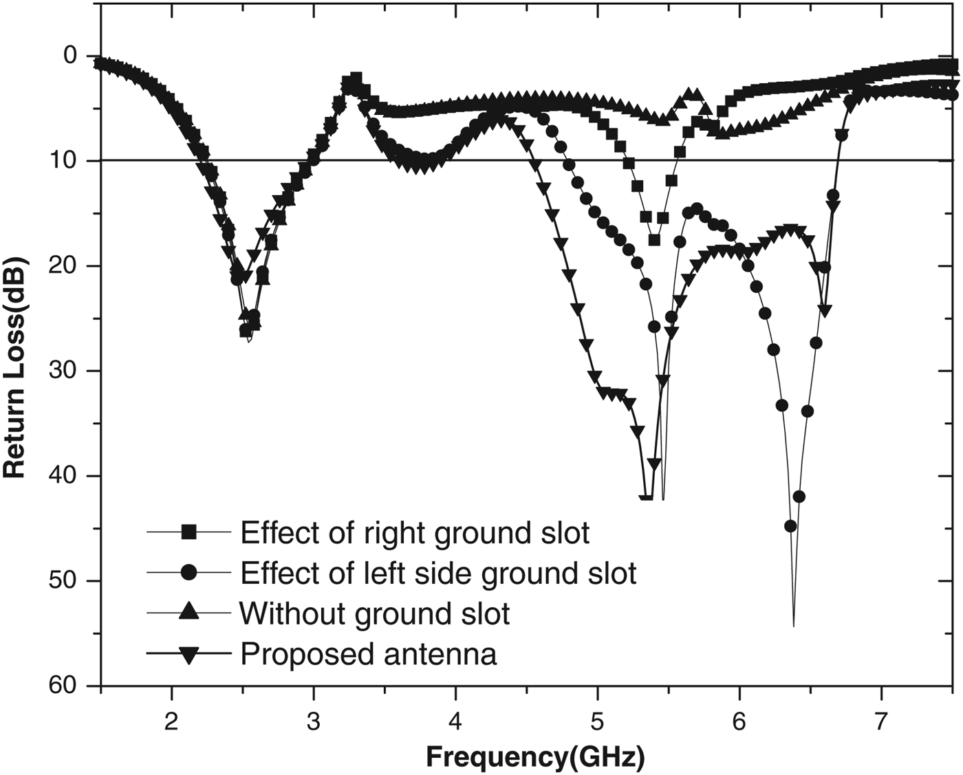
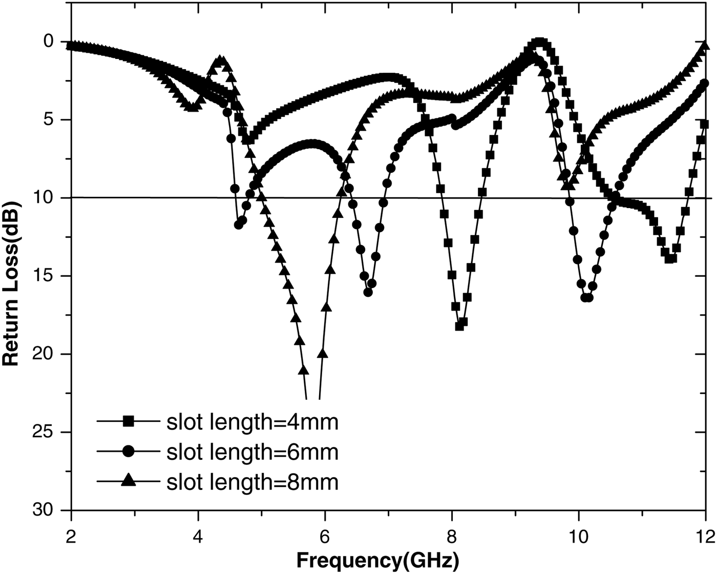
The effect of cutting slots in CPW ground plane is also studied. Figure 7 shows the effect of simulated return loss of the proposed antenna as a function of frequency with and without slots in the ground plane. It has been examined that without slots in ground plane, there is no upper frequency band. After including defects in ground plane a wide frequency band is obtained at upper frequency band. It is also observed from the simulation results study that slots do not have much impact on lower frequency band but higher frequency band is highly affected by slots in ground plane. It is also examined from the simulation results study that if we make slot only on right side of the ground plane, we get a small band at upper frequency band but after including defect on left side of the ground plane, we could get a wide frequency band at upper frequency band. We also studied the effect of varying slot lengths in ground plane as shown in Fig. 8. In this study, only basic T-shape structure with defected ground plane is considered. It can be seen from the results that as we increase the length of slots, frequency band shifts toward the lower frequency side. From the results of slot length variation, we can also say that DGS-based CPW feed helps in size reduction of antenna.
Fig. 7. Effects of ground plane defects on proposed antenna.
Fig. 8. Effects of slot length in ground plane on proposed antenna.
The current distributions at two resonant frequencies of 2.6 and 5.58 GHz are depicted in Fig. 9. It can be seen from the graph that four vertical arms of the proposed antenna are mainly responsible for lower frequency band of operation while the upper frequency band is due to basic T-shape structure with DGS and small current flow around a few horizontal strips.
Fig. 9. Current distributions at frequency (a) 2.6 GHz and (b) 5.58 GHz.
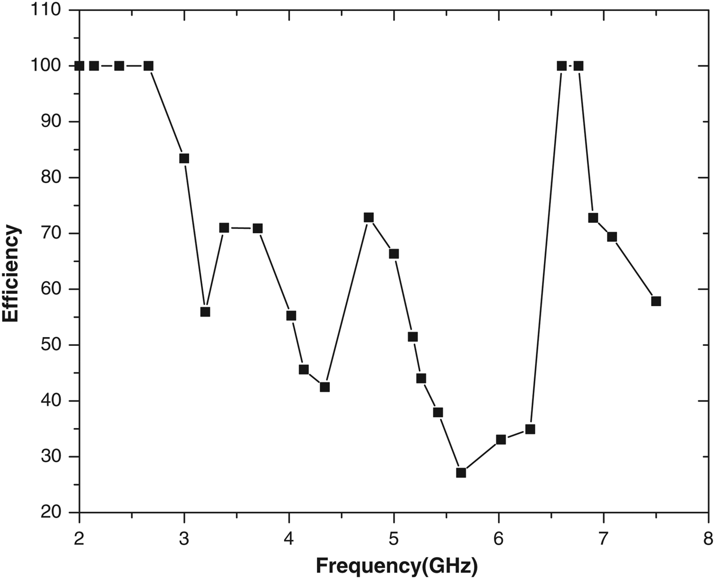
The simulated and measured normalized radiation patterns cut in the elevation plane (y–z) is shown in Fig. 10(a) and cut in the azimuthal plane (x–y) is shown in Fig. 10(b) for the proposed antenna at upper frequency band of 5.7 GHz. The radiation pattern obtained in the x–y plane is nearly omni-directional, and that in the elevation plane is all similar to monopole kind of antenna. Radiation performance of the antenna is acceptable at all the frequency bands. The simulation study indicates that the maximum antenna radiation efficiency is approximately 100% at 6.6 GHz as depicted in Fig. 11.
Fig. 10. Normalized radiation pattern of proposed antenna at 5.7 GHz. (a) Elevation plane and (b) Azimuthal plane.
Fig. 11. Radiation efficiency of the proposed antenna.
IV. CONCLUSIONS
In this study, a CPW-fed planar monopole antenna with a four vertical monopoles with horizontally displaced brick has been proposed, designed, fabricated, and tested for multiband operation using DGS technique. The proposed antenna was characterized in terms of the return loss, radiation pattern, current distribution, gain, and radiation efficiency. The simulated result shows an impedance bandwidth of 29% of lower frequency band, ranging from 2.232 to 3.1 GHz, with respect to the central frequency of 2.6 GHz, and the bandwidth of the upper frequency band is 2.1 GHz (4.712–6.81 GHz), or about 35%, with respect to the central frequency of 5.7 GHz. In addition, a parametric study has also been performed to facilitate the design and optimization process. The parametric study shows the effects of four vertical arms, connecting horizontal strips, and defects in the ground structure. The stable radiation patterns and good antenna gain over the operating bands has been observed and suitable for heterogeneous wireless communication applications. If some of the horizontal connecting metallic strips are substituted with a PIN diodes or micro-electro-mechanical (MEM) switch, then this antenna can achieve frequency reconfigurability by simply switching ON the required set of PIN diodes or MEM switches for the desired applications.
Davinder Parkash was born in Haryana, India in 1976. He received B.Tech. and M.Tech. degrees from the Department of Electronics and Communication Engineering at Kurukshetra University, Kurukshetra and NIT, Kurukshetra in 1999 and 2007, respectively. He is currently working toward a Ph.D. degree at Thapar University, Patiala. He is currently working as an Associate Professor and M.Tech. Coordinator at Department of ECE at Haryana College of Technology and Management, Haryana. Presently, he is also working as a Branch-Counselor of the IEEE student chapter. He received the ‘Young Scientist Award’ from the Governor of Punjab (India). He has published more than 45 papers in national and international journals/conferences. He is the Member of IEEE (Since 2010) and Member of Microwave Theory and Technique society membership no.-90859628 and member of Antenna Propagation Society. His main research interest includes the analysis and design of microstrip antenna, DGS technique, RFID antenna, and Wireless Communication.
Dr. Rajesh Khanna was born in Ambala (Haryana), India. He received B.Sc. (Engg.) degree in Electronics & Communication in 1988 from Regional Engineering College, Kurukshetra and M.E. degree in 1998 from Indian Institute of Sciences, Bangalore. He was with Hartron R&D centre till 1993. Until 1999, he was in All India Radio as an Assistant Station Engineer. Presently, he is working as a Professor in the Department of Electronics & Communication at Thapar Institute of Engineering & Technology, Patiala. He has published 120 papers in national and international journals/conferences. He has worth Rs 1.5 crore projects to his credits. His main research interest includes the analysis and design of microstrip antennas, Wireless Communication, MIMO, and Fractional Fourier transform-based wireless systems.