I. INTRODUCTION
The future generation of mobile phones will certainly exploit the numerous advantages of opportunistic cognitive radio concepts. Indeed, a flexible system, aware of its immediate environment through sensing operating modes and dynamic reconfiguration properties, will offer greatest services and performances; it will therefore become possible to dynamically and autonomously adjust radio operating parameters depending on available and collaborating wireless and wired networks, then offering improved nomadism and ubiquitous performances. [Reference Harada1]
Access to such improved flexibility involves specific constraints on the RF and digital interfaces of mobile devices for optimizing the communication interfaces. In this context, the aim is to consider and to design the RF sub-system to be as simple as possible (especially concerning filtering stages and the selection part of operating standards) and to ensure analog/digital (A/D) and digital/analog (D/A) conversion operations as closely as possible to the antenna to enhance the digital reconfigurability of the system. The idea of this multi-access antenna is to enable the management of these multiple parallel access ports for both transmission/reception modes directly by software. The structure, in addition to simplifying the radio frequency (RF) part (improved isolation between adjacent frequency bands, selective ports, size, etc.), is suitable for multistandard operations and more generally for the implementation of the SDR (Software Defined Radio) in an opportunistic context.
In a multistandard context, classical radio architectures use two types of antenna structures:
– Multiband antennas with one access port (PIFA i.e. [Reference Liu and Hall2, Reference Liu, Hall and Wake3], Patch i.e. [Reference Maci, Bifi Gentili and Avitabile4], Meandered i.e. [Reference Tang5], etc.). In this case, RF filtering remains necessary, which induces limitations in terms of complexity, noise, performances and therefore, reliability with the SDR approach (Fig. 1(a)).
– Multi-access antennas, with channels selection using switches – i.e. [Reference Mak6] (Fig. 1(b)). This frequency band selection method induces constraints on the input impedance of the non-activated access ports (open circuit (OC) terminations usually for proper matching conditions), which is not quite always feasible in practice under wideband operating conditions.

Fig. 1. Comparison between different architectures in a multistandard context. (a) Bi-band antenna with selective filtering input stage. (b) Bi-band antenna with selective switching structure. (c) Proposed architecture with two-access ports antenna and direct conversion (RF front ends without filter or switch).
Furthermore, this switching system limits the flexibility of the system dedicated to the SDR, including the operations of spectrum sensing (services availability survey) and real-time programming.
In this paper, the innovation of the proposed approach (Fig. 1(c)) consists in considering a two-access ports 50 Ω simultaneously matched antenna, with a quasi-omnidirectional radiation pattern, and then allowing direct-software standards selectivity and management without any switching or filtering operations. This approach is also compatible with radio front-end global integration on mature SiGe-type technologies.
II. ANTENNA DESIGN
A) Description of the structure
The antenna (see Fig. 2) is performed on a Rogers 4003 substrate (ε r = 3.38) of dimensions 40.25 × 95 × 0.508 mm3. A slot is etched on the upper 40.25 × 43 mm2 metallization level; two lumped feeding ports are inserted along one edge of this rectangular structure, each apart from the open-end extremities of the slot. Each of this access corresponds to a specific resonating mode, which can be selected independently from each other depending on the applied matching conditions. Consequently, we have a bi-access structure, with a potential bi-band behavior depending on the excitation structure.

Fig. 2. Model of the antenna.
Two microstrip stubs (in Fig. 2) are connected to the access ports 1 and 2; these stubs ensure the isolation of each of the operating modes towards the other [Reference Minard, Chambelin and Louzir7]. A capacitance (C = 1 pF) is placed in series with port 1 to ensure the matching condition at its own operating frequency. A 40.25 × 50 mm2 ground plane is realized on the left side of the substrate lower level. The simulations were carried out using Ansoft/HFSS™, considering lumped port-type excitations. The results are presented in Fig. 4.
B) Analysis and operating principles
The objective is to design an antenna with two isolated ports, each operating at its own resonance frequency (f 1 for port 1 and f 2 for port 2). Such an achievement requires that the access port 1 (and respectively the access port 2) at frequency f 1 (and respectively at frequency f 2) is matched to 50 Ω, while the second access is loaded using an equivalent short circuit (SC) at f 1 (and respectively at f 2) (Fig. 3). The principle is explained in detail in Section II.C.

Fig. 3. Isolation principle of the two ports.
We can observe in Fig. 4 that for the operating mode 1 {port 1: excited, port 2: 50 Ω (port 2 is loaded by a 50 Ω impedance but we always have the condition that the equivalent impedance of port 2 at f 1 is an (SC) impedance as we explained before)}, the resonant frequency is f 1 = 1.23 GHz (relative bandwidth #4% at ROS = 2). For mode 2 {port 2: excited, port 1: 50 Ω}, the resonant frequency is f 2 = 2.16 GHz (relative bandwidth #16% at ROS = 2). A 12 dB isolation value – see S 21 parameter in Fig. 4 (30 dB respectively) between the access ports is obtained over the f 1 frequency band (and the f 2 frequency band, respectively), well above the 10 dB expected isolation threshold.

Fig. 4. Coupling and reflexion coefficients on the two accesses.
The dimensions D 2 and D 3 of the slot (Fig. 5) affect the frequency response of the antenna. We therefore proceed with a parametric simulation as a function of the slot lengths D 2 and D 3 for the antenna without the isolation circuit since it mainly contributes to the matching and isolation conditions, independently from the frequency resonances.

Fig. 5. Dimensions of the slot.
This parametric simulation was done according to antenna 1 (antenna 2, respectively) – see Fig. 3 – to study the influence of D 2 and D 3 on f 1 (and respectively on f 2). The results are reported in Fig. 6.

Fig. 6. Effect of D 2 and D 3 on (a) f 1 for antenna 1 (b) f 2 for antenna 2.
Referring to Fig. 6, the frequency f 1 is controlled by the distances D 2 and D 3, whereas f 2 is controlled by D 3 only. Figure 7 shows the current density distribution in the two excitation configurations. It confirms that f 1 is controlled by the distance D 2+D 3, and f 2 is controlled by D 3, the maximum current density being distributed along the D 2+D 3 path length for f 1 excitation conditions, and being concentrated along the D 3 path length for f 2 excitation conditions. This figure also shows that the radiating part of the structure is essentially related to the slot; the dimensions of the surrounding rectangular metallic parts (upper “patch” and the ground plane) influence the input impedance of the antenna (matching).

Fig. 7. Current density distribution.
C) Open and SC stubs: incidence
We consider two operating frequencies (f 1 on port 1 – f 2 on port 2) so that f 2 ≈ 2f 1. This choice is quite advantageous since both stubs have a dual behavior on ports 1 and 2 at f 1 and f 2, respectively.
A short circuited (SC) termination is chosen for the λ g/2 stub 1 (connected on port 1) at f 2 (and consequently λ g/4 at f 1). This length is selected so as to ensure SC conditions on port 1 at f 2, and OC conditions at f 1, simultaneously. Perfect matching and isolation situations can therefore be simultaneously obtained on the access port 1 at f 1 and f 2, respectively.
An open-circuited (OC) termination is considered for the stub 2 – (λ g/2 long at f 2) connected on port 2, guarantying its transparency at frequency f 2 (OC at f 2) while providing the expected isolation at f 1 (SC at f 1), simultaneously. Fig. 8 summarizes this principle.

Fig. 8. Operating principle of stubs 1 and 2.
In addition to their fundamental role in inter-frequency band isolation, the two stubs, in association with the capacitance C, constitute a matching circuit over the whole operating bandwidths for both ports. The SC stub (dimensions: 1 × 40.7 mm2) has a characteristic impedance Z c1 = 55 Ω, whereas the OC stub 2 (dimensions: 4 × 40.7 mm2) has a characteristic impedance Z c2 = 20 Ω. This lower impedance value contributes to improve the f 2-frequency band matching conditions, while enhancing the isolation level between ports 1 and 2.
III. PROTOTYPING AND MEASUREMENTS
A) Prototype
The antenna has been optimized and processed on a ε r = 3.38 Rogers™ substrate (thickness h = 0.508 mm/tg δ = 0.0027). The prototype is presented in Fig. 9(a) (before mounting the 1 pF SMD capacitance and reporting the SMA™ coaxial connectors). Fig. 9(b) shows the feeding technique experimentally considered for properly exciting the antenna access ports: the central core of each coaxial cable is connected to the appropriate access ports 1 and 2 of the metallic radiating element, while their metal shielding are grounded.

Fig. 9. Prototype of the antenna (a) without excitation (b) with excitation.
B) Measurement's results and analysis
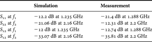
After assembling, we proceed to the S parameters measurements using a Vectorial Network Analyzer (VNA HP_8753ES, 30 kHz–6 GHz). The results are compared with those of the simulation in Fig. 10. Table 1 shows S parameters magnitudes at f 1 and f 2 for both simulation and measurement. The slight discrepancy is due to some approximation in the modeling of the lumped elements and cables and the PCB's solder mask; cables cause an extension of the ground plane changing slightly the input impedance, thus changing the values of return loss parameters (S 11 and S 22), and increasing slightly the coupling between the two ports, thus increasing the value of S 12.

Fig. 10. Comparison between measurement and simulation.
Table 1. Simulation and measurement.

IV. GENERALIZATION OF THE DESIGN METHOD FOR A RADIO-OPPORTUNISTIC APPROACH
A) Realization methodology
In the context of multiport antennas, the challenge lies in the isolation of adjacent access ports at different frequency bands (as well as within the same frequency band for multiports spatial sensing for instance). A relevant method is to realize a generic antenna with as many different ports as required for exciting appropriate expected operating modes and frequencies (method of characteristic modes of an antenna [Reference Cabedo-Fabres8, Reference Harrington and Mautz9]). Then, we add isolation and matching network independently from the radiating element that supports various excitation ports. Thus, the antenna can be assumed to be a lossy multipole structure, in which circuit performances (inter-bands inter-ports isolations and multiport return loss) can be optimized through this additional passive feeding network using the ADSTM software (Advanced Design System from AgilentTM).
B) Optimization method
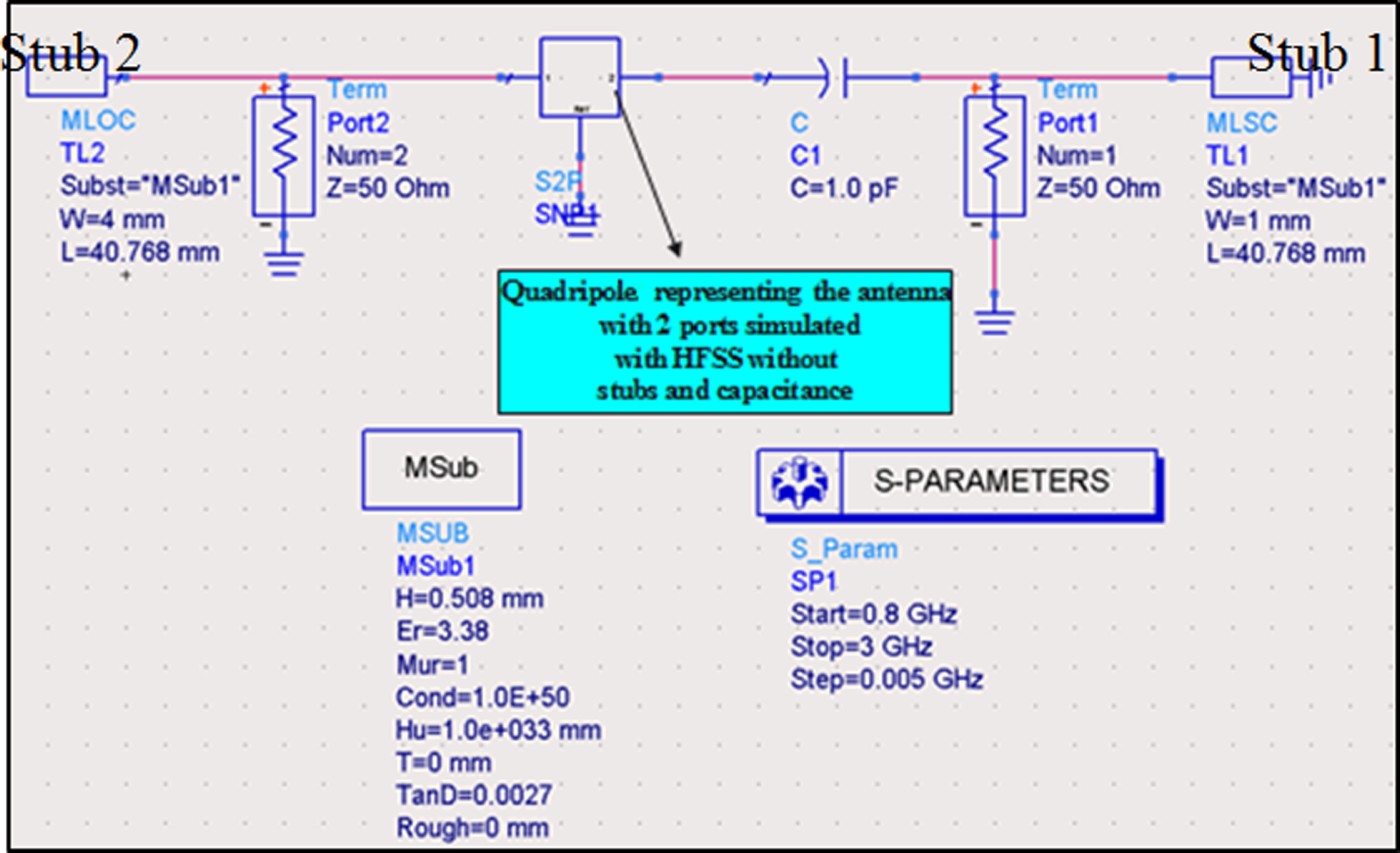
This section applies the methodology presented in Section IV.A on the above-mentioned antenna structure. A simulation of the radiating element alone (without the capacitance and stubs) is performed on an EM-simulator (HFSS from AnsoftTM) to recover the [S] parameters of the quadripole antenna (two access ports). Then, the capacitance and the matching structures (stubs and capacitance) are added to this quadripole on ADS (Fig. 11).

Fig. 11. Circuit simulation of the antenna.
We compare in Fig. 12 the results provided considering both hybrid (HFSS + ADS) and global (HFSS) electromagnetic simulations. We also consider the effect of the coaxial excitation cables connected to ports 1 and 2.

Fig. 12. Comparison of ADS, HFSS, and measurement.
The curves show the correspondence between the EM simulations, circuit simulations, and measurements of all S parameters. This validates the design and optimization methodology. The discrepancy on ADS is due to the fact that the EM coupling is not taken into account with the circuit simulation.
V. RADIATION PATTERNS
We present in Fig. 13, the convention of angles and in Fig. 14, the radiation patterns in terms of directivity in the (xoz, φ = 0°) and (yoz, φ = 90°) reference planes at f 1 (port 1: excited, port 2:50 Ω) and at f 2 (port 2: excited, port 1: 50 Ω) operating frequencies. The quasi-omnidirectional shape of the diagram in both (xoz) and (yoz) planes for both operating modes makes this antenna suitable for an opportunistic radio mobile communication. The directivity is about +2 dBi for both modes, with a measured maximum gain around 0 dBi, thus leading to an average 60% antenna efficiency. We note that the maximum gain is stable on the frequency band for each mode of operation because the antenna efficiency and the directivity are almost constant over these bands. A linear polarization is observed for the two modes, perpendicular to the (xoz) plane.

Fig. 13. Angle's convention.

Fig. 14. Radiation patterns.
VI. CONCLUSION
A new antenna structure with two accesses simultaneously matched and isolated on two different functional frequencies is presented. It offers new prospects in the reconfigurability of antennas once digitally controlled after direct A/D conversion, and leads toward a compromise between cost/performance criteria for an RF chain operating over a wide frequency range. This structure has been produced and tested in order to compare measurements and simulations. An application of this antenna could be the simultaneous transmission/reception of the two Wi-Fi standards, IEEE 802.11 g (f 1 = 2.4 GHz) and IEEE 802.11a (f 2 = 5 GHz ≈ 2f 1).
An n-access antenna is being considered now. The method of characteristic modes will be considered for identifying the location of accesses before implementing feeding multiport network for controlling isolation and matching performances. Thus, a multistandard and multi-access antenna will be implemented and configured for a radio communication system based on opportunistic cognitive radio.
ACKNOWLEDGEMENTS
This work is part of the TERROP project (Opportunistic Radio Terminals) under the financial support of the National Research Agency (ANR) and the Inter-Carnot collaborative program in collaboration with the Fraunhofer Institute in Germany.
 Walid El Hajj was born in Baassir – Barja, Lebanon, on April 25, 1985. He received his degree in Electric & Electronic Engineering (Telecommunication & Computer speciality) from the Lebanese University, Faculty of Engineering, Beirut-Lebanon, in 2008. He received a National Degree of Master for research in “Microwave materials and devices for communication systems” from TELECOM BRETAGNE, Brest – France, in 2008. Since 2009, he is a Ph.D. student in Lab-STICC/MOM laboratory in the Microwave Departement in TELECOM BRETAGNE.
 François Gallée received a Ph.D. degree in electronics from the University of Brest, Brest, France, in 2001. From 2001 to 2007, he was a research engineer in ANTENNESSA. His main research interest included antenna design. Currently, he is an Associate Professor within the Microwave Department, TELECOM BRETAGNE/TELECOM INSTITUT. He currently conducts research with the LABSTICC “Laboratoire en sciences et technologies de l'information, de la communication et de la connaissance”, associated with the National Research Scientific Council. His research concerns the development of new technologies for microwave and millimetre-wave applications and systems.
 Christian Person received the Ph.D. degree in electronics from the University of Brest, Brest, France, in 1994.
Since 1991, he has been an Assistant Professor with the Microwave Department, Ecole Nationale Supérieure des Télécommunications de Bretagne, Brest, France. In 2003, he became a Professor with the Telecom Institute/Telecom Bretagne, Brest, France, where he currently conducts research with the Information and Communication Science and Technology Laboratory (Lab-STICC). He is involved in the development of new technologies for microwave and millimeter-wave applications and systems. His activities are especially focused on the design of passive functions (filters, couplers) and antennas, providing original solutions in terms of synthesis techniques, analysis, and optimization procedures as well as technological implementation (foam, plastic, LTCC, etc.). He is also concerned with RF-integrated front-ends on Si, and he is presently involved in different research programs dealing with SoC/SiP antennas and reconfigurable structures for smart systems.