


I. INTRODUCTION
Three-dimensional (3D) multi-layer technologies such as low temperature co-fired ceramics (LTCC) [Reference Jantunen, Kangasvieri, Vähäkangas and Leppävuori1] or high-density multi-layers printed circuit board (HD-PCB) [Reference Li2] are currently being strongly developed because they offer considerable size reduction as well as the embedded function possibilities. For microwave applications such as filters, couplers, diplexers, etc. [Reference Abdul-Gaffoor, Smith, Kishk and Glisson3, Reference Cadiou4], these 3D structures offer new design possibilities for frequencies up to 100 GHz.
HD-PCB structures consist of several metal layers separated by dielectric substrates. The vias and microvias used in multilayer PCBs allow connecting lines of different metallic levels together or connecting devices to the power and ground plane [Reference Mathis, Peterson and Butler5]. The different metal planes can also be connected together with metallic plated through holes (PTHs). With the rise of working frequencies, the stacked multilayer PCB structures are subjected to electromagnetic phenomena like standing waves in cavities or like coupling and interaction between neighboring components.
As example of HD-PCB technology, the AT&S™ (PCB manufacturer) technology used during MIDIMU-HD project funded by the Euripides council is presented in Fig. 1. This HD multilayer consists of eight metallic layers (30 µm thickness) separated by Megtron6 (Panasonic™) substrate of ~95 µm thickness (depending on the metal densities of each level) and with a relative permittivity ε r = 3.3 and loss tangent tan(δ) = 0.0065 at 40 GHz. A single microvia hole consists of a central cylinder with a diameter of 140 µm, a conductor pad with a diameter of 240 µm, and when this via passes through a metallic plane it will also have a clearance hole called anti-pad of diameter of 350 µm. AT&S is able to stack more than three microvias and to realize buried via with diameter of 200 µm. The PTHs connecting the metal level M1 to the metal level M8 are 200 µm of diameter.

Fig. 1. AT&S: Eight metal layers stack and microvia realization for MIDIMU-HD project.
Obviously, these multilayer structures which involve parallel planes, dielectric layers, pads, and anti-pads are not ideal transmission components at high frequencies. The electrical behavior of a microvia can be modeled by serial inductance and resistance like is done for a metallic wire [Reference Wang and Harrington6, Reference Kwon7]. The vias and microvias may cause mismatch [Reference Kwon7], crosstalk, reflections, some additional signal delays, and consequently the degradation of signal performance. On the other hand, the coupling between vias, microvias, and parallel plates also plays an important role in the electrical performances of the via transition [Reference Rimolo-donadio8, Reference Schuster, Kwark, Selli and Muthana9]. The excitation of the parallel plate modes results in conversion of energy between propagation on line and propagation on guided plated structures which imply some transmission zeros.
In this paper, the effects of vias crossing a multilayer HD-PCB structure for microwave applications up to 45 GHz are analyzed and modeled using simple and intuitive equivalent circuits. For more accuracy, the concept of effective dimensions of the parallel-plates cavity is introduced to take into account the cavity boundary conditions. So, the proposed model is able to translate boundary behaviors like the classical ideal boundaries (perfect electric conductor (PEC) or perfect magnetic conductor (PMC)) [Reference Schuster, Kwark, Selli and Muthana9–Reference Heinrich and Dickmann11] as well as more realistic ones like open boundaries or PTHs shielded boundaries not really considered before. The proposed equivalent circuits are based on transmission line models, lumped elements (R, L, and C) for via modeling, and matrix impedances for the via – cavity couplings. They do not need any current-controlled sources or any voltage-controlled sources [Reference Schuster, Kwark, Selli and Muthana9, Reference Ndip10] and they are quite similar to the physical structures. So, the use of these equivalent circuits can facilitate the understanding of physical phenomena and help to overcome dysfunction due to via parallel-plates couplings. They were obtained thanks to using isolation resistances to describe behavior of floating grounds in circuit simulator software like advance design system (ADS) (Keysight™) and the use of impedance matrix to represent the coupling between vias and the cavities.
This paper is organized as follows. In Section II, the effects and the behaviors of microvias crossing a plated structure, are illustrated using electromagnetic (EM) simulations. Then, a physics-based circuit model associated with effective dimensions to characterize the interaction between the microvias and the parallel-plate modes is proposed in Section III. This modeling is implemented in Keysight-ADS™ software and validated by comparison with high frequency structural simulator (HFSS) (ANSYS™) finite element method (FEM) simulations and measurements in the fourth part of this paper. In Section V, we give some conclusions and we present some prospects of these studies.
II. COUPLING BETWEEN MICROVIAS AND PARALLEL PLATES
The interaction between microvias and parallel-plate cavities is illustrated by the study of the S parameters on a back-to-back transition using two stacked microvias to connect two microstrip access placed at metal level M1 to an embedded stripline placed at metal level M3 (presented in Fig. 1). The microvias go through metallic ground M2 of the microstrip lines. Two boundary condition cases have been considered for the rectangular cavity composed of the metal planes M2 and M4: (i) the open case (Fig. 2) and (ii) the case where boundaries are realized with PTHs (Fig. 3). The S parameters up to 50 GHz obtained using EM HFSS™ simulator for these two structures are presented in Figs 2(b) and 3(b). The S parameters show transmission zeros and perturbations which appear at different frequencies considering the boundary conditions. For example, the first perturbation appears around 10 GHz for the open boundary condition case, while it occurs within higher frequencies (up to 25 GHz) for PTH shielded cases. These perturbations are due to the coupling between the microvias and the cavity formed by the metallic plates as confirmed by the mapping of the electric field in the structure at the resonance frequencies where the electric field is distributed overall the cavity.
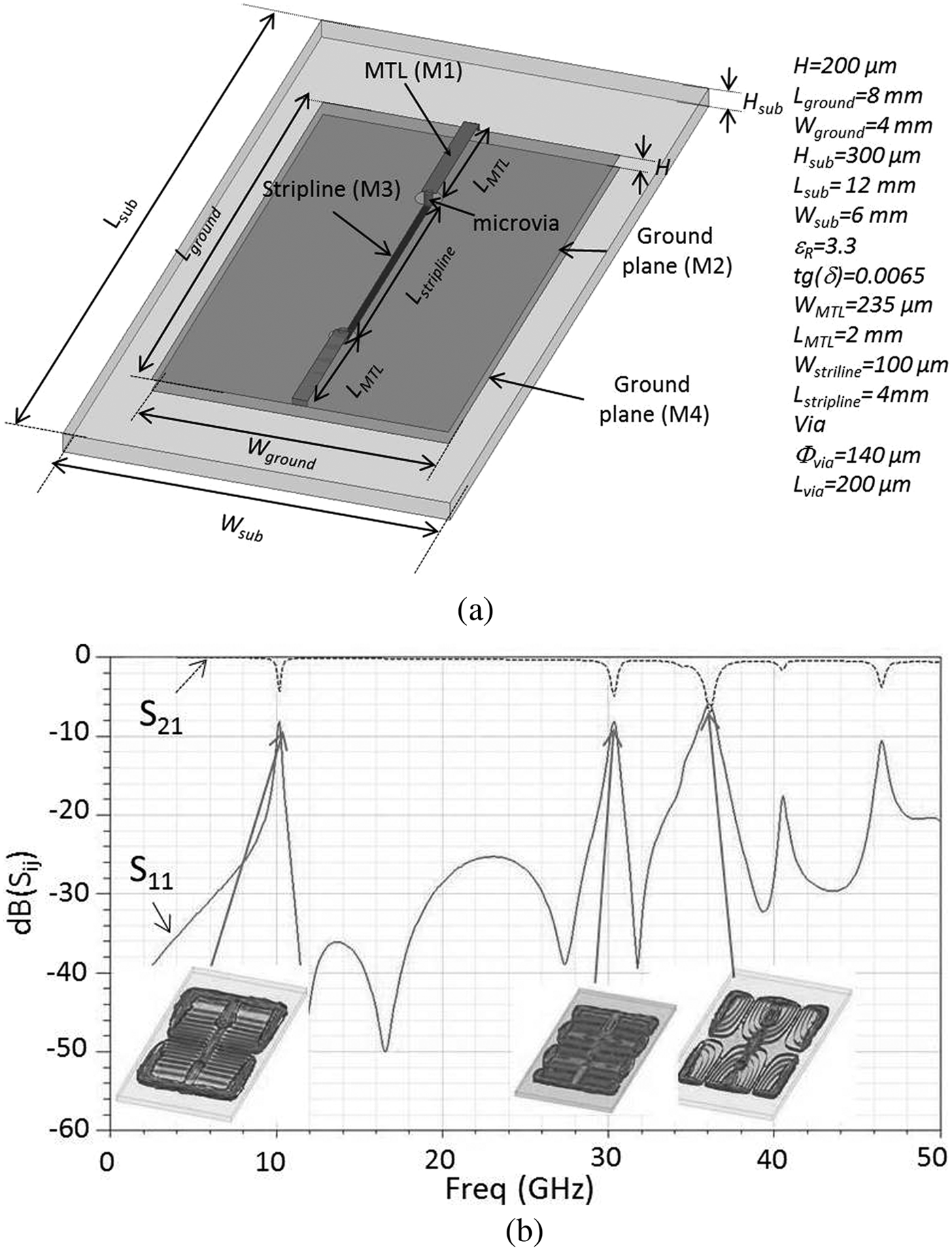
Fig. 2. (a) Back-to-back microstrip to stripline transition with open boundary conditions, (b) S parameter measurement results.

Fig. 3. (a) Back-to-back microstrip to stripline transition with PTHs shielded boundary conditions, (b) S parameter measurement results.
These examples demonstrate the interest to predict the perturbation risks and so to dispose of good models of interaction between vias and parallel-plate cavities, considering several boundary conditions. To save time during design and to limit the use of time consuming EM-simulators, a circuit model based on an analytical formulation of interaction between vias and parallel-plate cavities has been developed and it will be presented in the next section.
III. INTERACTION MODELING BETWEEN VIA-HOLES AND PARALLEL METAL PLATES
The modeling of the excitation of the parallel plates mode by a via crossing it, has been previously studied by a few authors [Reference Schuster, Kwark, Selli and Muthana9–Reference Heinrich and Dickmann11]. To illustrate how the coupling is done, let us analyze the current path in a transition by using via hole, between two microstrip lines situated on either side of two metal planes, as shown in Fig. 4(a).
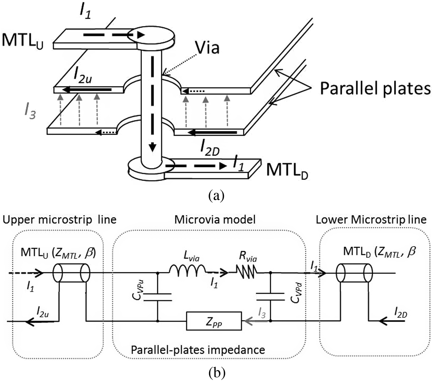
Fig. 4. Via through two grounded metallic planes and the corresponding equivalent circuit: (a) structure and (b) equivalent circuit.
The direct current I 1 flows through the upper microstrip line, then goes through the metallic via-hole and finally through the lower line. This current generates a return current I 2 in the two metallic planes which are the ground of the microstrip lines as shown in Fig. 4. To complete the current path, a current I 3 must exist between the upper and lower metallic planes. This current is flowing through the impedance called parallel-plate impedance “Z PP” which is the image of the modes which may exist between the two conductor plates. So, this structure can be modeled by the equivalent circuit proposed in Fig 4(b).
In this equivalent electrical schematic (Fig. 4(b)), “C VPu,d” represents the capacitance between the via-hole and the upper or lower metallic plate, respectively [Reference Wang and Harrington6], “L Via” and “R Via” are, respectively, the inductance and the resistance of the via-hole [Reference Rimolo-donadio8]. There are several papers addressing the estimation of these parameters [Reference Wang and Harrington6, Reference Heinrich and Dickmann11, Reference Pajovic, Yu, Potocnik and Bhobe12] with the help of analytical formulas. Another way to determine these values is to use static electromagnetic simulation tool like Q3D extractor (ANSYS™). The impedance “Z PP” represents all the modes in the parallel-plate cavities between the two metallic planes and it can be obtained by solving the 2D Helmholtz equation with appropriate boundary conditions on the periphery of the cavity. “Z MTL” and “β” are the characteristic impedance and the wave number of the microstrip lines [Reference Heinrich and Dickmann11].
According to a more general case with further ports, the concept of parallel-plates impedance can be extended with use of parallel plate impedances matrix relating all the ports together. Figure 5 presents a general two ports structure which is composed of two rectangular metallic planes of lateral dimensions Wx × Wy separated by a substrate of height “H” and permittivity “ε R”. The ports are etched apertures on the upper face presenting a width “p xi × p yi” and placed at coordinates (x pi, ypi), where the subscript “i” is the port number. The matrix impedance [Z PP] which represents the interaction between all ports across parallel-plates when all the propagated modes are taken into account, can be expressed in Cartesian coordinates by [Reference Ndip10, Reference Tao, Hong and Tang13]:
 $${Z_{PPij}} = \displaystyle{{j\omega \mu H} \over {{W_{xeff}}{W_{yeff}}}}\mathop \sum \limits_{m = 0}^{m = + \infty} \mathop \sum \limits_{n = 0}^{n = + \infty} \displaystyle{{C_m^2. C_n^2. F_{BCx}^2. F_{BCy}^2. {F_{pi}}{F_{pj}}} \over {k_{xm}^2 + k_{yn}^2 - {k^2}}},$$
where  $C_m^2, C_n^2 = 1\; $ for m,n = 0 and
  $C_m^2, C_n^2 = 2$ or m,n ≠ 0. The cut-off wave number according to the x and y axes are given by: k xm = mπ/W x, k yn = nπ/W y, and wave number in the homogeneous lossy media:
 $$k = \omega \sqrt {\varepsilon \mu} \left( {1 - j\left( {\displaystyle{{\tan \left( \delta \right) - \left( {{\delta _s}/H} \right)} \over 2}} \right)} \right),$$
where tan(δ) is the dielectric losses tangent and electric conductor loss are given by  ${\delta _s} = \sqrt {2/\omega {\mu _c}{\sigma _c}} $.

Fig. 5. Geometry of two parallel plates.
For ideal boundaries condition like PEC or PMC, the boundaries functions F BCξ (the subscript ξ denote the axis x or y) take into account the boundary lateral border of the parallel planes and they can be expressed by [Reference Schuster, Kwark, Selli and Muthana9]:
 $$\left\{ {\matrix{ {{{\rm F}_{BC\xi}} = \sin \left( {{k_i}\xi} \right){\rm \; \; \; for\; \;} ({\rm PEC}),{\rm \;}} \cr {{{\rm F}_{BC\xi}} = \cos ({k_i}\xi ){\rm \; \; for\; \;} ({\rm PMC})} \cr}} \right.$$
with i = m for x axis direction, or i = n for the y-axis direction and where ξ = x pi or y piare the port coordinates. Notice that equation (1) allows the [Z PP] determination in all cases, whether the boundaries along the axis “x” or “y” are the same or not.
The function describing the port area influence is given by:
 $${F_{pi}} = {\rm sinc}\left( {\displaystyle{{{k_m}.{p_x}} \over 2}} \right).{\rm sinc}\left( {\displaystyle{{{k_n}.{p_y}} \over 2}} \right).$$
In many applications, the boundaries are not clearly defined as PEC or PMC. For example, if we consider two metallic planes on a larger substrate (like in Fig. 2(a)), the boundary conditions cannot be considered as a PMC because of the fringing effect of electric fields. On the other hand, if we consider parallel plates shielded by using PTHs (e.g. in Fig. 3(a)), the cavity boundaries are not a perfect electrical conductor due to electric field configuration on PTHs boundaries. So, to complete previous studies [Reference Schuster, Kwark, Selli and Muthana9–Reference Heinrich and Dickmann11], the use of effective dimensions W effx and W effy instead of the real physical dimensions W x and W y has been introduced. In a general case, the effective cavity dimensions can be expressed as:
 $${W_{eff}} = W + dW$$
For the open boundaries case (e.g. Fig. 2(a)) to take into account the overflowing of the electric field on boundaries, using the well-known microstrip approach [Reference Gupta14], the corrective term dW can be expressed by:
 $$dW = 0.41 \times H\displaystyle{{\left( {{\varepsilon _R} + 0.3} \right)\left( {W/H + 0.264} \right)} \over {\left( {{\varepsilon _R} - 0.258} \right)\left( {W/H + 0.8} \right)}},$$
where H is the substrate thickness, W represents W x or W y according to the considered axis, and ε R is the relative permittivity of the substrate. The PMC boundary function can be used with this corrected dimension W eff. This corrective term resulted from a quasi-static approach and must be adapted to express dispersive behavior for large thickness substrates.
In the case of PTH shielded boundaries (e.g. Fig. 3(a)), the corrective term dW to take into account the containing of electric field, can also be estimated using the well-known theory of substrate intergrated waveguide (SIW) [Reference Tao, Hong and Tang13] and given by:
 $$dW = - 1.08\displaystyle{{{d^2}} \over s} + 0.1\displaystyle{{{d^2}} \over W},$$
where “d” is the diameter of the PTH and “s” is the space between two consecutive via-holes center and “W” is for W x or W y depending on the considered direction. This approach is very accurate until s/d is smaller than three [Reference Xu and Wu15]. The PEC boundary function must then be used with the effective dimension W eff.
This approach of effective dimensions can be used considering different boundary conditions along the x and y axes. As an example, a PTH shielded boundary can be considered along the x-axis, while an open boundary can be considered along the y-axis.
A “Matlab™” program has been developed to determine the frequency-dependent impedance matrix [Z PP] whatever the boundary conditions. This impedance matrix is saved in “touchstone” format easily readable by circuit simulators like ADS.
To demonstrate the interest of using effective dimensions in case of non-ideal boundaries, Fig. 6 shows the transmission parameters S 21 determined with EM simulation, of a transition between two microstrip lines through a rectangular parallel plates cavity (W x = 60 mm, W y = 40 mm, H = 254 µm, and ε R = 3.6). The results obtained by considering open boundaries or PTHs shielded boundaries (d = 200 µm and s = 400 µm) are compared with those obtained using perfect PMC and PEC boundaries, respectively. The results of the simulations of the equivalent circuit of Fig. 4(b) where effective size of the cavity are considered are also plotted in Fig. 6. One should note that there is a difference of about 2–5% between frequencies of the apparition of the zeros by considering the real boundary conditions (open or PTH shielded) rather the perfect ones (PMC or PEC). A very good agreement can be observed between EM simulations with open or PTHs shielded boundaries and circuit model results for the both cases. Finally, the results in Fig. 6 confirm that the use of effective dimensions leads to more accurate results whatever the boundary conditions. In the next paragraph, other validations of the proposed modeling are illustrated.
Fig. 6. Transmission coefficient of one via crossing a parallel-plates cavity: (a) open boundaries and (b) PTH shielded boundaries.
IV. MODEL VALIDATION BY COMPARISON WITH FULL-WAVE SIMULATIONS AND MEASUREMENTS
First, the accuracy of the proposed model is illustrated on a back-to-back microstrip to stripline transition with two kinds of boundaries: (a) with open boundaries (see Figs 2(a) and 2 (b)) with PTH boundaries (see Fig. 3(a)). The equivalent model valid for both boundary cases is presented in Fig. 7. This equivalent circuit was implanted in ADS© software. In this equivalent model, isolation impedances with great value of 50 GΩ have been introduced to overcome the problem of ground reference used in circuit simulator software and to be able to express the floating grounds behavior. The matrix [Z PP] link currents and voltages at these ports, which are isolated to the ground reference, so the isolation impedances do not have any influence on it. This matrix expresses all the standing waves existing between the two grounds M2 and M4 around the stripline. For both boundary cases, the values of microvia model (L = 46 pH, R = 0.7 Ω, C 1 = 16 fF, and C 2 = 20 fF) have been obtained using Q3D Extractor© software for a 40 GHz frequency. The inductance model is a lossy inductance model from ADS.
Fig. 7. Circuit model for a back-to-back microstrip to stripline transition.
The comparisons of S parameters obtained with EM simulation (HFSS) and those obtained using the circuit model are shown in Fig. 8. For both cases of boundaries, a good agreement between our modeling results and those obtained using EM simulations can be observed. For the open boundary case the small shift for higher frequencies is due to the proposed correction dW (equation (6)) which does not take into account the dispersive behavior.
Fig. 8. Modeled S parameters for a back-to-back microstrip to stripline transition: (a) open boundaries case and (b) PTHs shielded boundaries case.
A multilayer structure with different boundary conditions for the parallel-plate cavities has also been studied using EM simulations. It consists in a back-to-back microstrip to stripline transition where the microvias are crossing two parallel-plate cavities. The dimensions of the structure are presented in Fig. 9. For the upper cavity, open boundary conditions were taken into account and for the lower cavity, PTHs (d = 200 µm and s = 400 µm) shielded boundary were considered. The equivalent circuit used to model this structure is shown in Fig. 10. Two parallel-plates matrix impedances ([Z PPU] and [Z PPL]) were used to model the interaction between vias and the parallel-plate cavities. For structures with more than one or two layers, an impedance matrix has to be determined for each cavity achieved between two metallic layers. These impedance matrices are then connected to the different ground planes of the different lines as it is done for the case of two cavities in Fig. 10. The values of via characteristics were obtained using Q3D extractor. For this example, the value of the resistive part of via inductance was R VIA = 0.5 Ω and this value had only small influence on the simulated response.
Fig. 9. Back-to-back microstrip to stripline transition with via crossing a parallel-plate cavity with different boundary conditions (Open for the upper cavity and PTHs shielded for the lower).
Fig. 10. Equivalent circuit of a back-to-back microstrip to stripline transition where via crossing two different cavities.
The comparison of EM results and circuit simulation are presented in Fig. 11. A good agreement can be observed despite a small frequency shift for higher frequencies. This frequency shift can be due to non-dispersive model of equivalent dimensions especially for the open cavity case (the upper one). Nevertheless, the proposed model and equivalent circuit are able to well describe the behavior of a multilayer structure with complex boundary conditions.
Fig. 11. S parameters of a back-to-back microstrip to stripline transition where the vias crossing to different cavities.
A last example consists of an embedded stripline stub filter realized using the AT&S technology. The filter was placed at metal level M3 of a eight layers structure and it is excited by microstrip lines at level M1 and two stacked microvias (diameter ϕ = 140 µm) going through the ground M2 as illustrated in Fig. 12(a). The metallic level M4 was a full ground plane and a parallel-plates cavity existed between levels M2 and M4. The cavity was shielded with PTHs boundaries (d = 200 µ and s = 400 µm). The filter was designed to present a 30 GHz central frequency and a 50% relative bandwidth. The equivalent circuit model is shown in Fig. 12(b). The use of isolation impedance of 50 GΩ allows to directly employ the [Z PP] matrix describing the behavior of cavity formed by M2 and M4 floating ground planes. The value of the parasitic elements depict the microvias influence were obtained using the Q3D extractor. Microvias and transmission line values as well as filter stub-characteristics are resumed in Table 1.
Fig. 12. Embedded stripline filter structure and equivalent circuit: (a) filter structure and (b) equivalent circuit.
Table 1. Characteristics of access lines, filter lines and stubs, and microvia model.
The S parameters of this filter were measured using a probe station and thru reflect line (TRL) calibration. The reference planes are shown in Fig. 12(a). The comparison between measurement results and circuit modeled responses are presented in Fig. 13. A good agreement between measurement results and circuit simulation ones can be observed over the all frequency bandwidth. The frequency discrepancy observed for the high frequency can be attributed to the manufacturing tolerances, to the simplicity of the available models of lines which do not take into account the dispersive behavior and to the fact to neglect the vias connecting the stubs to the both grounds M2 and M4 which can perturb the fields in the cavity. Nevertheless the simply circuit model provides good approximations and it is able to predict suitably the transmission zeros in the filter bandwidth.
Fig. 13. S parameter responses of the PTH shielded stripline filter.
These three examples prove the usefulness and the accuracy of the proposed model of coupling between vias or microvias and parallel-plate cavities in multilayer structures.
V. CONCLUSION
In the first part of this paper, the effects of the coupling between vias and microvias and cavities created by multi-level metal planes in multilayer structures like LTCC or HD-PCB have been outlined. Then, in order to take into account these parasitic effects, a tool based on the determination of impedance matrix of parallel planes [Z PP] has been proposed. To express the non-ideal character of some boundaries like open or PTHs shielded boundary conditions the notion of effective dimensions considering the E-field mapping in the cavity have been introduced. The development of simple, intuitive and physical equivalent circuits has been also proposed. These models can be very useful to quickly predict and understand the behavior of multilayer structures which include many vias, microvias, PTHs, and parallel-plates. Finally, the parallel-plates impedance matrix associated with the intuitive equivalent circuit has been validated by using several comparisons with results obtained by EM simulations and measurements. Using this approach, good results have been obtained until 40 GHz for the open boundaries cases and until 50 GHz for PTH shielded boundary cases. As a future prospect, we intend to develop model for more complex shapes of cavities, to be able to simulate a lot of realistic multilayer structures. We will also work to propose a dispersion approach for open boundary to be able to better describe the behavior beyond 40 GHz.
Thierry Le Gouguec was born in Vannes, France, in 1966. He received the Ph.D. degree in Electrical Engineering from the University of Brest, Brest, France in 1994. Since 1995 he has been an Assistant Professor at the University of Brest and he conducts research at the Laboratory Lab-STICC which is affiliated with the French National Science Research Centre (CNRS). He is the author or co-author of more than 30 papers published in reviewed journal or presented at international conferences. His research interests include Electromagnetic Compatibility (EMC), the interconnect characterization, the new RF, and wireless interconnect concepts for Inter-Chip communications and the small printed antennas.
Najib Mahdi received the Ph.D. degree in Electronics and Microwaves, optics photonics from the Science Faculty of Limoges, France, in 2012. He is currently a postdoctoral researcher and teaching at the University of Brest, France. His research interest includes the development of microwave components/circuits and characterization of metal/wireless interconnections for Inter-Chip Data Communication.
Stéphane Cadiou has received his Ph.D. in Electronics from the University of Brest in 2007. He has worked as a research engineer for Euripides MIDIMU-HD project from 2011 to 2013. He is an RF R&D Engineer in Thales Communications & Security. His main focus concerns the RF filters and SIW technologies.
Cédric Quendo (M'03) was born in Plouay, France, in 1974. He received the Electrical Engineer degree and the Ph.D. degree in Electrical Engineering from the University of Brest, France, in 1999 and 2001, respectively. Between 2001 and 2010, he gave courses and conducted research in several institutes and he was notably visiting researcher in 2005 at Georgia Tech, Atlanta, USA. Since 2010, he is a Professor with the Electronic Department, University of Brest, France. He also conducts research with Microwaves Group of the Lab-STICC Laboratory, France. His research activities principally concern the modeling and design of microwave devices for microwave and millimeter-wave applications.
Erich Schlaffer is an Austrian citizen with a technical college for electrical engineering in Kapfenberg. He joined as a Process Engineer of AT&S in December 1998 and was responsible as the Department Head for mechanical drilling, laser drilling, routing, and electrical test. Out of this experience he started to work on Concepts for Radio Frequency PCB́s as Project Leader within the R&D department.
W. Pessl, is a Quality Engineer at AT&S Leoben and he works on Concepts for Radio Frequency PCB's.
A. Lefevre is an Engineer at Thales Communications and Security and he is the leader of The Euripides MIDIMU-HD project.


