


Introduction
Metamaterials are artificial materials with simultaneous permittivity and permeability negatives [Reference Veselago1–Reference Shelby, Smith and Schultz3]. These materials can be manufactured by using distributed elements (microstrip lines) [Reference Sanada, Caloz and Itoh4–Reference Xu, Wang, Qing Qi, Lv and Gao9] as well as with lumped-elements inductance L and capacitance C [Reference Eleftheriades10–Reference Caloz, Ahn and Itoh13]. The demonstration of the behavior of several metamaterial-based microwave devices requires the development of numerical methods or the use of commercial software, allowing the computation of the distribution of the electromagnetic field. However, in the case of lumped circuits’ software simulators, this distribution is allowed only on small-sized periodic circuits presenting a few number of unit cells. In fact, for the example of the well-known commercial simulator ADS (Advanced Design System), the distribution of both voltage and current on periodically L–C lumped network, which is equivalent to electric and magnetic field distributions, requires the definition of all nodes in the periodic network and should be labeled as observation nodes. This requirement is extremely time- and memory-consuming for large periodic circuits. The transmission-matrix method (TMM) can be considered as an efficient method to overcome the limitations of ADS [Reference Caloz, Ahn and Itoh13, Reference Ma, Cui, Chin and Cheng14]. In fact, it does not necessitate to label the nodes of the periodic circuit as observation nodes. However, the TMM is well practicable for regular-shaped circuits where the filling of numerical matrix with the same elements is easy. The TMM's analysis of large circuits also needs the multiplication of large matrices, which makes the method unstable [Reference Ma, Cui, Chin and Cheng14]. An iterative wave concept iterative process (WCIP) method based on the concept of waves can overcome all the limitations of the methods quoted above. The WCIP method, which is almost used near two decades in the electromagnetic analysis of planar microstrip microwave circuits [Reference Baudrand and N'gongo15–Reference Hajlaoui, Trabelsi and Baudrand18], is recently used in a novel approach to analyze quasi-periodic lumped circuits [Reference Elbellili, Azizi, Latrach, Trabelsi, Gharsallah and Baudrand19–Reference Azizi, Latrach, Raveu, Gharsallah and Baudrand23]. These periodic lumped circuits can be considered as good equivalent representations to accurately model continuous mediums if the cell's length is much smaller than the guided wavelength. This condition helps to consider both voltage and current as quasi-static along a unit cell, hence the possibility of applying Kirchhoff's laws to find the electrical relations inside a unit cell. These equivalent models are constructed by means of a basic unit cell which contains the lumped elements, i.e. capacity, inductance and resistance.
Metamaterial-based lenses which are modeled by periodic lumped circuits oblige the engineer to be conscious of several parameters [Reference Grbic and Eleftheriades24, Reference Shen, Foteinopoulou, Kafesaki, Koschny, Ozbay, Economou and Soukoulis25]. One of the parameters which must be determined with more importance is the characteristic impedance. Generally, this impedance not only depends on the elements L and C of a unit cell but also on frequency. A mismatch between various mediums constituting the optical system could cause losses of energy and thereafter losses in the resolution of the lens. For that reason, one must obtain the variation of Bloch impedance according to the frequency, which helps to take the suitable value of the characteristic impedance at such frequency. Another important parameter is the location of the exciting source which should be in the near field of the lens to permit the enhancement of the evanescent modes. In fact, the spatial spectrum of the source radiation can be expanded into propagating modes and evanescent modes. The propagating modes can travel from the source plan to the focal plan through the optical system without disturbances. However, if the source is far from the lens, the evanescent modes will be lost before reaching the desired destination, which leads to losses in the resolution of the image. The negative refractive index (NRI) lens presents a solution to amplify the evanescent waves for a super-resolution imaging system.
This paper is organized as follows:
Firstly, it presents the developed equations of the novel approach of the WCIP method which can be easily programmed. Then, it presents a validation of the suggested approach by introducing some examples of lumped-circuit-based applications where the results of analysis by WCIP can be justified theoretically. Besides, it proves the effectiveness of the novel approach by the study of metamaterial-based lenses in near- and far-field imaging. Finally, it shows the analysis of quasi-parabolic lens as an irregular-shaped periodic circuit application.
The basic theory of the WCIP method
The iterative process WCIP is based on the concept of waves (incident/reflected waves A and B) in two domains (spectral and spatial) as given by the system of equation (1)
 $$\left\{ \matrix{A = SB + A_0\quad spatial\,domain \hfill \cr B = \Gamma A\quad spectral\,domain \hfill} \right..$$
where S, Γ, and A 0 are the spatial reflection coefficient, the spectral reflection coefficient, and the incident wave excited by the feeding source, respectively.
The schematic diagram of the iterative process is shown in Fig. 1.

Fig. 1. The iterative process. The abbreviations used in the diagram are: spat, spatial; spec, spectral; FFT, fast Fourier transform; FFT−1, the inverse fast Fourier transform.
The running of the iterative process, which requires the determination of A0, Γ, and S, is finished after a certain number of iterations representing its convergence as explained by Fig. 1 and the system of equation (2)
 $$\left\{ \matrix{B^1 = \Gamma. A_0\quad 1^{rst}iteration \hfill \cr A^1 = S.B^1 + A_0 \hfill \cr B^2 = \Gamma. A^1\quad 2^{nd}\,iteration \hfill \cr A^2 = S.B^2 + A_0 \hfill \cr. \hfill \cr. \hfill \cr. B^n = \Gamma. A^{n - 1}\quad n^{th}iteration \hfill \cr A^n = S.B^n + A_0 \hfill} \right..$$
Determination of the incident wave A0
Figure 2 shows the general schema of the periodic circuit which has a characteristic impedance Z0 and a feeding source E0.

Fig. 2. General schematic of periodic circuit excited by E0.
We can rewrite the voltage and current at the input of the first cell in terms of the incident and reflected waves, as follows (3)
 $$\eqalign{& V_0 = \sqrt {Z_0} (A_0 + B_0). \cr & I_0 = \displaystyle{1 \over {\sqrt {Z_0}}} (A_0 - B_0)}$$
We can also write (4)
 $$V_0 = E_0 - Z_0I_0.$$
Hence, we can deduce A 0 as (5)
 $$A_0 = \displaystyle{{E_0} \over {2\sqrt {Z_0}}}.$$
Determination of the spectral reflection coefficient Г
A two-dimensional (2D) periodic lumped circuit can be established by repeating a basic unit cell along the x, y axis. So, the calculation of the parameters concerns only one unit cell. The mathematic and electrical relations inside a unit cell should be written in general forms to give more flexibility in the way periodic circuits are analyzed. Thus, the capacitance or inductance should be replaced by an auxiliary source, as depicted in Fig. 3.

Fig. 3. (a) L–C unit-cell circuit, (b) equivalent circuit using auxiliary sources.
Based on Floquet's theorem and Kirchhoff's laws, the electrical relations inside a unit cell can be expressed by the system of equation (6), as follows
 $$\left\{ \matrix{Ix + Iy + Iz - Ixe^{\,j\alpha} - Iye^{\,j\beta} = 0 \hfill \cr Vx.e^{\,j\alpha} = Vy.e^{\,j\beta} = Ez \hfill \cr Vx + Ex - rIx - Ez = 0 \hfill \cr Vy + Ey - rIy - Ez = 0 \hfill} \right.,$$
where α and β are the spatial phase shifts between two cells along x and y axis.
The phase shift α and β can be written, as follows (7)
 $$\eqalign{& \alpha (m) = \displaystyle{{2\pi \,m} \over M}\quad ;\quad \beta (n) = \displaystyle{{2\pi \,n} \over N} \cr & With\quad M = \displaystyle{{Dx} \over {dx}}\quad ;\quad N = \displaystyle{{Dy} \over {dy}}\quad ;\quad M,\,N \in \,IN,}$$
where Dx and Dy are the dimensions of the periodic circuit.
We can rewrite (6) in a matrix form as in (8), which gives the admittance matrix that relates the vector of currents to the vector of voltages (auxiliary sources).
 $$\left \vert \matrix{Ix \cr Iy \cr Iz} \right \vert = \displaystyle{1 \over r}\left \vert \!\!\!\!\!\!\!\!\!\!\!\!\!\!\!\!\!\!\!\!\!\!\!\!\matrix { 1\quad 0\quad a \cr 0\quad 1\quad b \cr \quad \quad \quad \quad a^*\quad b^*\quad \left \vert a \right \vert ^2 + \left \vert b \right \vert ^2} \right \vert \left \vert \matrix{Ex \cr Ey \cr Ez } \right \vert,$$
where
 $$a = e^{ - j\alpha} (1 - e^{\,j\alpha} );\quad b = e^{ - j\beta} (1 - e^{\,j\beta} ).$$
After the calculation of the Eigen values and the Eigen vectors of the admittance matrix, we can rewrite the admittance matrix, as follows (9)
 $$\bar Y = \displaystyle{1 \over r}(YY^ + + (1 + \left \vert a \right \vert ^2 + \left \vert b \right \vert ^2)ZZ^ + ),$$
Y + and Z + are the transpose of the complex conjugate of vectors Y and Z (10) in an orthonormal base. The developed equations are cited in [Reference Azizi, Baudrand, Elbellili and Gharsallah22]
 $$Y = \left( \matrix{\displaystyle{{ - b^ *} \over {\sqrt {{\left \vert a \right \vert} ^2 + {\left \vert b \right \vert} ^2 + 1}}} \cr \displaystyle{{b^ *} \over {\sqrt {{\left \vert a \right \vert} ^2 + {\left \vert b \right \vert} ^2 + 1}}} \cr 0} \right)$$
 $$Z = \left( \matrix{\displaystyle{a \over {\sqrt {{\left \vert a \right \vert} ^2 + {\left \vert b \right \vert} ^2}. \sqrt {{\left \vert a \right \vert} ^2 + {\left \vert b \right \vert} ^2 + 1}}} \cr \displaystyle{b \over {\sqrt {{\left \vert a \right \vert} ^2 + {\left \vert b \right \vert} ^2}. \sqrt {{\left \vert a \right \vert} ^2 + {\left \vert b \right \vert} ^2 + 1}}} \cr \displaystyle{{\sqrt {{\left \vert a \right \vert} ^2 + {\left \vert b \right \vert} ^2}} \over {\sqrt {{\left \vert a \right \vert} ^2 + {\left \vert b \right \vert} ^2}. \sqrt {{\left \vert a \right \vert} ^2 + {\left \vert b \right \vert} ^2 + 1}}} } \right).$$
The spectral reflection coefficient is then given by (11), such that
 $$\Gamma = \displaystyle{{1 - Z_0\bar Y} \over {1 + Z_0\bar Y}}.$$
When r tends towards 0, Γ can be rewritten as follows (12)
 $$\Gamma = 1 - 2YY^ + - 2ZZ^ +.$$
Determination of the reflection spatial coefficient S
The spatial reflection coefficient SΔ along Δ axis, where Δ = (X, Y, Z), is given by (13)
 $$S_\Delta = \displaystyle{{Z_\Delta - Z_0} \over {Z_\Delta + Z_0}},$$
where Z 0 is the characteristic impedance.
Generally, we can define three types of cells for a periodic circuit, namely a source cell (s), a transmission line cell (t), and a load cell (c). Hence, the values of the spatial reflection coefficients according to the three types of cells are expressed as follows (14)
 $$S_{x,y,z} = (Vals,\,Valt,\,Valc)_{x,y,z}.$$
In general, writing the spatial reflection coefficient requires the definition of three functions: Hs, Ht, and Hc (15). These functions test the type of the unit cell present at the space coordinates (i, j).
 $$\eqalign{& Hs_{(i,j)} = \left\{ \matrix{1:\,\,presence\,of\,a\,source\,cell \hfill \cr {\rm 0:}\,else \hfill} \right. \cr & Ht_{(i,j)} = \left\{ \matrix{1:\,\,presence\,of\,a\,TL\,cell \hfill \cr {\rm 0:}\,else \hfill} \right. \cr & Hc_{(i,j)} = \left\{ \matrix{1:\,\,presence\,of\,a\,load\,cell \hfill \cr {\rm 0:}\,else \hfill} \right..}$$
Then, the spatial reflection coefficient S on each cell (i, j) is written as follows (16)
 $$\eqalign{S_{x,y,z}(i,j) = & \, Hs\,(i,j).Vals_{x,y,z} \cr & + Ht\,(i,j).Valt_{x,y,z} \cr & + Hc\,(i,j).Valc\,\,(i,j)_{x,y,z}.}$$
We can rewrite equation (16) in a matrix form, such that (17)
 $$\left( \matrix{S_X \cr S_Y \cr S_Z } \right)_{(i,j)} = \left( \matrix{Vals_x\,Valt_x\,Valc_x \cr Vals_y\,Valt_y\,Valc_y \cr Vals_z\,Valt_z\,Valc_z } \right)\left( \matrix{Hs \cr Ht \cr Hc } \right)_{(i,j)}.$$
So, for each cell's coordinates (i,j), the spatial domain equation (1) can be rewritten as follows (18)
 $$\eqalign{\left( \matrix{A_x(i,j)\cr A_y(i,j)\cr A_z(i,j)} \right) & = \left( \matrix{A_{0x}(i,j) \cr A_{0y}(i,j) \cr A_{0z}(i,j)} \right) + \left( \matrix{S_x(i,j)\quad 0\quad 0 \cr \quad 0\quad S_y(i,j)\quad 0 \cr \quad 0\quad 0\quad S_z(i,j) } \right)\cr & \quad \times \left( \matrix{B_x(i,j) \cr B_y(i,j) \cr B_z(i,j) } \right)}.$$
It is clear from (12) and (18) that we have only used the third-order matrix to determine the waves A and B through a unit cell. The passage from one cell to another is done iteratively. However, the TMM requires the multiplication of high-order matrices for large periodic circuits.
After the convergence of the iterative process, we have directly calculated the voltage E and current J inside each cell using the following equation (19)
 $$\left\{ \matrix{E_{x,y,z} = \sqrt {Z0} (A_{x,y,z}(i,j) + B_{x,y,z}(i,j)) \hfill \cr J_{x,y,z} = \displaystyle{1 \over {\sqrt {Z0}}} (A_{x,y,z}(i,j) - B_{x,y,z}(i,j)) \hfill} \right..$$
Thus, we can deduce the impedance matrix Z of a two-port circuit as follows (20)
 $$Z = \sum\limits_{x,y} {\left( {\displaystyle{{E_{(x,y)}} \over {J_{(x,y)}}}} \right)}$$
Then, the scattering matrix is written as follows (21).
 $$\bar S = \left[ {Z - Z0} \right]\left[ {Z + Z0} \right]^{ - 1}.$$
Determination of the parameters of metamaterial modeling
Conventional homogenous materials or right-handed materials (RH) can be modeled by using distributed periodic L–C networks in which the per-unit-length capacitance C and inductance L represent a positive equivalent permittivity and permeability, respectively. The exchange of places between L and C permits to have the equivalent representation of metamaterials or left-handed materials (LH). The unit cells of the RH/LH equivalent periodic circuits are shown in Fig. 4.

Fig. 4. (a) 2D RH unit cell, (b) 2D LH unit cell.
For continuous mediums, the characteristic impedance Zc and the index of refraction could be expressed as a function of the permeability μ0 and permittivity ε0 of vacuum and the relative permeability μr and permittivity εr of the medium.
We can write the wave impedance and the refractive index, respectively, as follows (22) and (23)
 $$Z_0 = \sqrt {\displaystyle{{\mu _0\mu _r} \over {\varepsilon _0\varepsilon _r}}},$$
 $$n_{RH/LH} = \pm \sqrt {\mu _r\varepsilon _r}.$$
In the equivalent representations of continuous mediums, the inductance and the capacitance should be expressed as a function of the permittivity and permeability.
First, we start by writing the expressions of the propagation constants of the RH/LH mediums.
In equivalent representations of continuous mediums, the inductance and the capacitance should be expressed in function of permittivity and permeability.
We start by writing the expressions of propagation constants of the RH/LH mediums.
 $$\eqalign{\beta _{RH} = & \displaystyle{\omega \over {\Delta l}}\sqrt {L_RC_R} \cr \beta _{LH} = & - \displaystyle{1 \over {\omega \Delta l\sqrt {L_LC_L}}}.}$$
Hence, we deduce the refractive index as follows (25)
 $$n_{RH} = \displaystyle{c \over {V_\varphi}} = \displaystyle{{\sqrt {L_RC_R}} \over {\Delta l\sqrt {\mu _0\varepsilon _0}}},$$
 $$n_{LH} = \displaystyle{c \over {V_\varphi}} = - \displaystyle{1 \over {\omega ^2\Delta l\sqrt {\mu _0\varepsilon _0} \sqrt {L_LC_L}}}. $$
Then, the L and C parameters can be expressed as in (26) and (27), respectively
 $$L_R = \mu _0\mu _r\Delta \,l\,\,;\quad L_L = \displaystyle{1 \over {\omega ^2\varepsilon _0\left \vert {\varepsilon _r} \right \vert \Delta \,l}}\,\,,$$
 $$C_R = \varepsilon _0\varepsilon _r\Delta \,l\,\,;\quad C_L = \displaystyle{1 \over {\omega ^2\mu _0\left \vert {\mu _r} \right \vert \Delta \,l}},$$
where Δl is the length of a unit cell.
For a balanced composite RH/LH unit-cell circuit as depicted in Fig. 5(b), the refractive index is given by (28)
 $$\eqalign{n_{CRLH} = & n_{RH} + n_{LH} \cr = & \displaystyle{c \over {\Delta l}}\left( {\sqrt {L_RC_R} - \displaystyle{1 \over {\omega ^2\sqrt {L_LC_L}}}} \right).}$$
Fig. 5. (a) 2D CRLH periodic circuit, (b) 2D CRLH unit-cell circuit.
The Bloch impedance Z B is given by (29)
 $$Z_B = \displaystyle{{A_t - D_t \pm \sqrt {{(A_t + D_t)}^2 - 4}} \over {2C_t}},$$
where At, Ct and Dt represent the elements of the transfer matrix which is written for a symmetric unit cell as follows (30)
 $$\left[ \matrix{A_t\,\,B_t \cr C_t\,\,D_t } \right] = \left[ \matrix{1 + \displaystyle{{ZY} \over 2}\quad Z(1 + \displaystyle{{ZY} \over 4} \cr Y\quad \quad 1 + \displaystyle{{ZY} \over 2} } \right]\,\,\,.$$
Validation of the WCIP method
The validation of the WCIP method can be carried out according to three cases. In the first case, we have performed the variation of some scattering parameters for a 2D network. In the second one, we have showed the voltage distribution, respectively, along a transmission line containing a metamaterial section, and through a 2D RH network excited in its center by a voltage source. In the last one, we have checked the principle of negative refraction. The obtained results are illustrated by the theory.
Variation of scattering parameters
We consider a 12 × 12 CRLH unit-cell circuit which has 12/12 input/output ports, as depicted in Fig. 5(a). Each CRLH unit cell is shown in Fig. 5(b). The resistances of the horizontal and vertical limits of the periodic circuit are Zh = 50 Ω and Zv = ∞, respectively.
The simulation is performed with the following values: L R = L L = 2.5 nH; C R = C L = 1.0 pF. There is a good agreement between the WCIP simulation results and Ref in [Reference Caloz, Ahn and Itoh13], as illustrated by Figs 6(a) and 6(b).

Fig. 6. Variation of scattering parameters according to the frequency: (a) the transmission coefficient S 6, 24 (dashed line: WCIP; solid line: Ref [Reference Caloz, Ahn and Itoh13]); (b) the reflection coefficient S 66 (black: WCIP; gray: Ref [Reference Caloz, Ahn and Itoh13]).
Distribution of voltage through 1D/2D periodic lumped circuits
A conventional RH transmission line which contains a metamaterial LH section is depicted in Fig. 7. All the TL sections are considered with the same characteristic impedance Zc.

Fig. 7. A conventional transmission line containing metamaterial LH section.
The equivalent circuit is of 100 unit cells, where the length of each unit cell is Δl = 1 mm. The LH TL section is designed to be denser than the other RH sections by a factor of 2 and 3, respectively, as shown by Figs 8 and 9 where the metamaterial LH section is delimited by dashed lines.

Fig. 8. (a) Voltage (volts) and (b) phase (radians) distributions along1D metamaterial TL using WCIP method (n RH = 4; n LH = −8; f = 3 GHz, Zc = 377).

Fig. 9. (a) Voltage (volts) and (b) phase (radians) distributions along 1D metamaterial TL using WCIP method (n RH = 4; n LH = −12; f = 3 GHz, Zc = 377).
The expressions of the guided wavelength as a function of the unit-cell length (Δl) is given by (31)
 $$\eqalign{\left( {\displaystyle{{\lambda g} \over {\Delta l}}} \right)_{RH} = & \displaystyle{1 \over {\,f\sqrt {L_RC_R}}} \cr \left( {\displaystyle{{\lambda g} \over {\Delta l}}} \right)_{LH} = & 4\pi ^2f\sqrt {L_LC_L}.}$$
The values of the guided wavelengths that we can read in Figs 8 and 9 are the same as those calculated by equation (31). Thus, we respectively find out from the following quoted figures: (λg (RH) = 25 unit cells, λg (LH) = 12.5 unit cells) and (λg (RH) = 25 unit cells, λg (LH) = 8.3 unit cells).
Moreover, we can observe the change of the sign of the propagating wave at the interfaces (dashed lines) since the propagation constants have opposite signs, as it is indicated by equation (24).
Now, we consider a 512 × 512 unit-cell RH network excited at the center by a voltage source. We can see the generation of perfect propagating cylindrical waves around the source, as shown in Fig. 10.

Fig. 10. (a) Voltage (volts) and (b) phase (radians) distributions: (μr = 1, εr = 1, f = 1 GHz; Δl = 10 mm).
Verification of the concept of negative refraction
We consider a periodic circuit of 128 × 256 unit cells divided equally in two RH/LH parts. The excitation is done at the down left corner of the circuit.
The two mediums have the same characteristic impedance and the same index of refraction, but with opposite signs. According to Snell–Descartes law of refraction, the angle of refraction will be the same as that of the incidence. The opposite signs of these angles shown by Fig. 11 illustrate the principle of negative refraction since the RH/LH mediums have an index of refraction n RH = 1 and n LH = −1, respectively.
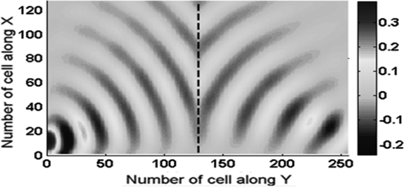
Fig. 11. Voltage (volts) distribution (f = 1.0 GHz, L R = 12.5 nH, C R = 88 fF, L L = 286 nH, C L = 2.0 pF).
Analysis of metamaterial flat lenses using WCIP method
Principle
The resolution of the image inside an optical imaging system depends on whether the source is near or far from the first interface of the lens, i.e. the near- and far-filed imaging cases.
In fact, the wave vector k is defined as follows (32)
 $$\eqalign{k^2 = & k_x^2 + k_z^2 \cr = & \left( {\displaystyle{{n\omega} \over c}} \right)^2,}$$
where k x and k z are the transverse and the longitudinal components of the wave vector k, respectively; n and c are the refractive index and the celerity of light in free space, respectively.
A propagating electric field depends on both space and time (z, t), as given by equation (33)
 $$E(z,t) = E_0e^{i(k_zz - \omega t)}.$$
Therefore,we can write the following equation (34)
 $$k_z = \pm \sqrt {{\left( {\displaystyle{{n\omega} \over c}} \right)}^2 - k_x^2}.$$
The ±sign indicates the phase propagation in ±Z directions.
Let us consider the positive Z direction, the longitudinal wave-vector component is then written as follows (35)
 $$k_z = \left\{ \matrix{i\sqrt {k_x^2 - {\left( {\displaystyle{{n\omega} \over c}} \right)}^2} \,\,;\quad k_x\rangle \displaystyle{{n\omega} \over c}\quad \to \,evanescent\,waves \hfill \cr \sqrt {{\left( {\displaystyle{{n\omega} \over c}} \right)}^2 - k_x^2} \,\,;\quad k_x \le \displaystyle{{n\omega} \over c}\quad \to \,propagatin\,g\,waves \hfill} \right..$$
High spatial-frequency waves are evanescent waves which decay exponentially in a positive refractive index (PRI) medium. However, these waves should grow exponentially in a NRI medium. Thus, we can discussthe evanescent waves following two cases: far-field and near-field imaging.
In the far-field imaging case, the source is far from the interface of lens with a distance of more than a wavelength. As a result, the evanescent waves will be lost before reaching the lens. So, we will not obtain a perfect image owing to the fact that only the propagating waves contribute to the formation of the source's image. However, in the case of near-field imaging, the source is close to the lens interface with a distance of less than a wavelength. The evanescent waves are then amplified by the NRI lens before being completely decayed. So, the evanescent waves and propagating waves establish a perfect image of the source. To conclude, the spatial resolution of the image is determined by the ability of the imaging system to transmit the higher spatial frequencies, i.e. the evanescent waves.
The proposed circuit of the metamaterial flat lens
A NRI medium represents the metamaterial flat lenses embedded between two PRI mediums, as depicted in Fig. 12. The total imaging system is a periodic circuit of 128 × 256 unit cells.

Fig. 12. Schematic circuit of the imaging principle by NRI flat lens.
Far-field imaging case
The first interface of the NRI flat lens is located between columns 82 and 83, the second interface is located between columns 117 and 118. The distance from the source to the first interface is d 1 = 18 cells and the width of the lens is d = d 1 + d 2 = 33 cells. The guided wavelength λg measures eight cells at 1.68 GHz, which gives d 1 = 2.25 λg and d = 4.125 λg as the thickness of lens.
The parameters of the RH/CRLH unit cells are the following: RH (C R = 177fF, L R = 25 nH); CRLH (C R = C L = 177 fF, L R = L L = 25 nH), ZB = 352Ω, f = 1.68 GHz.
The results of simulation using the WCIP method show the 2D and 3D views of voltage distributions, as described in Figs 13(a) and 13(b). These views present the source, the internal focus (first image) and the external refocus (second image). We can clearly see in Figs 13(c) and 13(d) that the two images have the same spatial shapes, which proves that their spectral expansions do not contain evanescent modes. Hence, there are no losses in the resolution of image 2 according to image 1. Yet, the evanescent modes contained in the source's spectrum are lost before reaching the first interface of the lens, which explains the difference between the spatial shapes of the sources and the two images.

Fig. 13. (a) 3D view of Abs (Ez); (b) 2D view of Real (Ez); (c) longitudinal view of Abs (Ez) at line 68; (d) transversal view of Abs(Ez) at columns 64, 102, and 134, i.e. the transverse plans of source, image 1, and image 2, respectively.
Near-field imaging case
The first interface of the NRI lens is located between columns 107 and 108, while the second interface is placed between columns 134 and 135, with a thickness of lens d = 27 cells. The distance from the source to the first interface is d 1 = 18 cells. The guided wavelength λg measures 30 cells at 1.0 GHz, which gives d 1 = 0.6 λg and d = 0.9 λg as the lens thickness.
The parameters of the RH/LH unit cells are as follows: RH (C R = 88.5fF, L R = 12.5 nH); LH (C L = 2.0 pF, L L = 286 nH); Z B = 375, f = 1 GHz.
Figure 14(b) shows the amplification of the evanescent waves by the NRI flat lens. These waves have reached the first interface before being lost. At that time, the propagating waves as well as the evanescent waves have participated in the formation of perfect images of the source, which is illustrated by Fig. 14(c) in which we can notice two almost perfect images of the source.

Fig. 14. (a) 2D view of Abs (Ez); (b) longitudinal view of Abs (Ez) at line 68; (c) transversal view of Abs (Ez) at columns 90, 126, and 144, i.e. the transverse plans of source, image 1, and image 2, respectively.
Another phenomenon that we can see at the lens interfaces (RH/LH interfaces) is the presence of surface plasmons. This phenomenon appears at the interface between RH/LH mediums having the same propagation constant magnitudes but with opposite signs. If these mediums are juxtaposed according to the Y direction, there will be no wave propagation along this direction which is considered as an open circuit since βy = 0 at the interface. However, βx≠0 at the interface, which allows the propagation of energy along the interface following the form of surface plasmon.
Analysis of arbitrary-shaped lumped circuit by WCIP
As an example of arbitrary NRI circuits, we present a quasi-parabolic LH lens which transforms a cylindrical wave to a plane wave. The schema of the proposed lens is depicted in Fig. 15.

Fig. 15. Schematic of the quasi-parabolic refractor (lens): the LH medium.
Figure 16 shows the WCIP simulation results for the following parameters: (C R = 124 fF, L R = 17.6 nH, C L = 672 fF, L L = 95.36 nH, f = 1 GHz), which gives the following refractive index: n RH = 1.4, n LH = −3.

Fig. 16. (a) Voltage (volts) and (b) phase (radians) distributions through the quasi-parabolic refractor.
Conclusion
In this paper, a novel approach of the iterative method WCIP was accurately used to demonstrate the negative refraction of electromagnetic waves and the perfect imaging by NRI flat lens using metamaterials. Conventional and metamaterial mediums are modeled by periodic lumped circuits. It is clear from the results of simulation of large periodic lumped circuits that WCIP method is computationally more efficient than ADS and TMM. In fact, WCIP is used to calculate the distribution of electromagnetic field through a periodic circuit of many hundred unit cells which can have an arbitrary-shaped geometry. So, we can say that we have resolved the problem of the nodes labeling when we use ADS simulator and the problem of stability when we use TMM.
 Taieb Elbellili was born in Kasserine, Tunisia, on April 29, 1980. He received the M.Sc degree on Electronic Systems from the Faculté des sciences de Tunis in 2006. Since 2015, he is working toward his Ph.D. His research focuses on computational electromagnetic methods and metamaterials modeling.
 Mohamed Karim AZIZI was born in Tunis, Tunisia, on December 26, 1979; he received the M.Sc degree on Telecommunications from SupCom in 2008. He received his Ph.D degree in Electronics from the Faculty of Sciences of Tunis, Tunisia 2013. He is currently an Associated Professor in the Department of Computer Sciences in the Higher Institute of Multimedia Arts of Mannouba, ISAMM, Tunisia. His research interest at present include metamaterials, metasurfaces, graphene antennas.
 Lassaad Latrach received the Master degree in Electronic Systems from the Faculte des Sciences de Tunis in 2006.He received his Ph.D degree in Electronics from the Faculty of Sciences of Tunis, Tunisia 2010. He is an Associated Professor in EMSI Mannouba Tunisia. His research interest include computational electromagnetic methods, passive and active circuits, antennas.
 Hichem Trabelsi was born in Tunisia, in 1962. He received the Ph.D. in Electronics from the University of Pierre & Marie Curie, Paris VI, France in 1991. He joined the Department of Physics at the Faculty of Sciences, Tunis, in 1992, where he is currently working on microwave active and passive filters and electromagnetic theory for solving field problems in microwave circuits.
 Henri Baudrand (SM′90–F′04–LF′14) received the Ph.D. degree in microwaves from the Institut National Polytechnique, Toulouse, France, in 1966. He is a Professor Emeritus with the Ecole Supérieure d'Electronique Electrotechnique Informatique, ENSEEIHT, National Polytechnic Institute of Toulouse, Toulouse, France. He has authored and coauthored six books: Introduction au calcul des éléments de circuits microondes, optimisation des circuits non linéaires, calcul des circuits microondes par les schémas équivalents (CEPADUES Editions Toulouse), New Trends and Concept in Microwave Theory and Technics, Adaptation de la méthode WCIP aux circuits SIW et SINRD: WCIP: Wave Concept Iterative Process, and Modélisation Globale des Circuits Electroniques Hautes Fréquences. He cosigned over 110 publications in journals, four chapters in scientific books, and 250 communications in international conferences. He is a Fellow Member of ‘Electromagnetism Academy’ and Senior Member of IEE Society. He was President of URSI France Commission B for 6 years (1993–1999), the IEEE-MTT-ED French chapter (1996–1998), and the International Comity of O.H.D. (Hertzian Optics and Dielectrics) between 2000 and 2004. He was the recipient of Officier des Palmes académiques and Doctor Honoris causa of lasi University (1996).


