Introduction
U.S.-based independent agency, Federal Communication Commission (FCC) has approved the usage of ultra-wideband (UWB) (3.1–10.6 GHz) as an unlicensed spectrum in 2002 [1]. UWB technology offers high performance and high security in both indoor and outdoor wireless communication systems. Currently, UWB technology is being used in various applications ranging from radar to high data-rate personal area network. Furthermore, it can also be used in both commercial and military applications. However, the wide frequency range of UWB may cause interference with the already existing licensed spectra such as WiMAX band (3.3–3.7 GHz), WLAN band (5.15–5.85 GHz), ITU-8 band (7.9–8.8 GHz), etc. Rejection capability of a UWB antenna is required to avoid interference from the abovementioned licensed frequency bands. In this regard, during the last few decades, antenna researchers have reported several methods for designing a compact UWB antenna with integrated band-notch filtering capability [Reference Pancera, Modotto, Locatelli, Pigozzo and Angelis2–Reference Kim, Kim, Park and Jo16].
Single-notch filtering functionality is realized by introducing different slot structures either in ground plane or in radiating patch. For example, an inverted L-shaped slot is included in the ground plane [Reference Pancera, Modotto, Locatelli, Pigozzo and Angelis2], while U-shaped [Reference Cho, Kim, Choi, Lee and Park3], W-shaped [Reference Chattha, Ishfaq, Saleem, Huang and Boyes4], hat-shaped [Reference Lee, Park and Lee5], and cup-shaped [Reference Lee and Park6] slots are incorporated in the radiating patch. Antennas with dual- [Reference Modirkhazeni, Rezaei and Lafmajani7–Reference Biswas, Ghatak, Karmakar and Poddar9], triple- [Reference Lin, Jin and Ziolkowski10, Reference Cai, Yang and Cai11], and quad- [Reference Mewara, Mahendra, Sharma and Deegwal12, Reference Wu, Wei, Shi and Li13] notched characteristics by using different combinations of various slots have also been reported. Although incorporation of slot structures is a simple and popular approach, other options such as introducing parasitic strips above the ground plane [Reference Islam, Azim and Mobashsher14], use of split-ring resonators [Reference Tang, Xiao, Deng, Wang, Guan, Wang and Ge15], and Hilbert curves [Reference Kim, Kim, Park and Jo16] are also found to be very effective at notch out the desired frequency band.
To establish a high data-rate communication link, RF engineers are still trying to stretch the impedance bandwidth beyond the specified UWB range. Toward this, different techniques such as inserting an inverted T-shaped notch in the ground plane [Reference Ojaroudi, Ghobadi and Nourinia17], by incorporating a pair of L-shaped conductor-backed planes, and a pair of modified L-shaped slots on the radiating patch [Reference Ojaroudi, Ojaroudi and Amir18], by using fractal structures such as Penta-Gasket-Koch [Reference Jahromi and Komjani19] and Sierpinski Carpet geometry [Reference Jahromi20], have been reported in various papers.
All of the abovementioned antennas have been designed on low-loss printed-circuit boards such as FR4-epoxy and Rogers RT/duroid 5880, and they are termed off-chip antennas. However, to meet the requirement of obtaining a compact system, research on designing antennas on a silicon substrate (generally termed on-chip antennas) is going to be the future trend. Such on-chip antennas can be easily integrated with other necessary digital and analog modules required for making a compact system-on-chip (SoC) [Reference Cheema and Shamim21]. Though most of the reported on-chip antennas are for 60 GHz communication [Reference Bao, Guo and Xiong22–Reference Yang, Ma, Yeo and Lim24], research on UWB antennas using silicon as a substrate is still rudimentary. In 2007, Yan et al. proposed an on-chip antenna for IEEE 802.11a and UWB applications [Reference Yan and Murch25]. Jiang et al. reported a novel complementary metal–oxide semiconductor (CMOS) process-based on-chip antenna that can be used in UWB wireless inter-/intra-connects or a wireless chip area network [Reference Jiang, Mao and Leung26]. Kimoto et al. demonstrated UWB signal transmission among silicon integrated circuits (ICs) using linear dipole antennas [Reference Kimoto and Kikkawa27]. UWB antenna on a silicon substrate with notched characteristics was first reported in [Reference Karmakar and Singh28]. Another coplanar waveguide (CPW)-fed UWB antenna on silicon substrate with dual band-notch characteristics was demonstrated in [Reference Awasthi, Sharma, Singh, Kumar and Kumari29].
In this paper, the proposed work mainly highlights two crucial aspects. The first one is to design a compact monopole antenna on silicon substrate with operating bandwidth extended beyond the specified UWB range. The next one is to incorporate band-notch filtering capability to mitigate interference from the 7.9–8.4 GHz band assigned by International Telecommunications Union (ITU) for X-band uplink satellite communication systems. This proposed antenna is compact as compared with the reported antenna structures in [Reference Pancera, Modotto, Locatelli, Pigozzo and Angelis2–Reference Jahromi20, Reference Karmakar and Singh28, Reference Awasthi, Sharma, Singh, Kumar and Kumari29]. It also provides large impedance bandwidth as compared with the related antennas published in [Reference Pancera, Modotto, Locatelli, Pigozzo and Angelis2–Reference Yan and Murch25, Reference Karmakar and Singh28, Reference Awasthi, Sharma, Singh, Kumar and Kumari29]. This compact antenna with higher bandwidth is suitable to meet the requirement for its applicability in the present short-range, high data-rate communication systems. Also, the proposed antenna designed on the Si substrate has the potential to be integrated with other modules on the same substrate using single process technology to make an application-specific, truly efficient, compact SoC at a reduced cost.
The rest of the paper is organized as follows. Detailed description of the antenna design steps is presented in the “Antenna design and analysis” section. The “Fabrication process” section gives the briefing of the fabrication process steps. Different performance parameters of the antenna in both frequency and time domain are demonstrated in the “Results and discussion” section. Finally, some concluding remarks are given in the “Conclusion” section.
Antenna design and analysis
The top view and 3D view of the proposed antenna structure are shown in Figs 1(a) and 1(b), respectively. It consists of an irregular octagonal patch with a spiral-shaped slot within it. Table 1 shows the optimized values of the corresponding design parameter. CPW feeding is preferred here over the microstrip line to avoid any kind of interference of the EM field with another IC component. This interference generally occurs when a ground plane is placed below the substrate [Reference Cheema and Shamim21]. The feedline with the G/W/G configuration of 0.51/1.4/0.51 (mm) is used to materialize 50 Ω impedance. An FEM-based EM simulator HFSS v17 is used to analyze the 3D antenna structure. The standard CMOS process with only one level of mask (metal patterning) has been used to realize the structure. Layered view of the antenna is shown in Fig. 2.
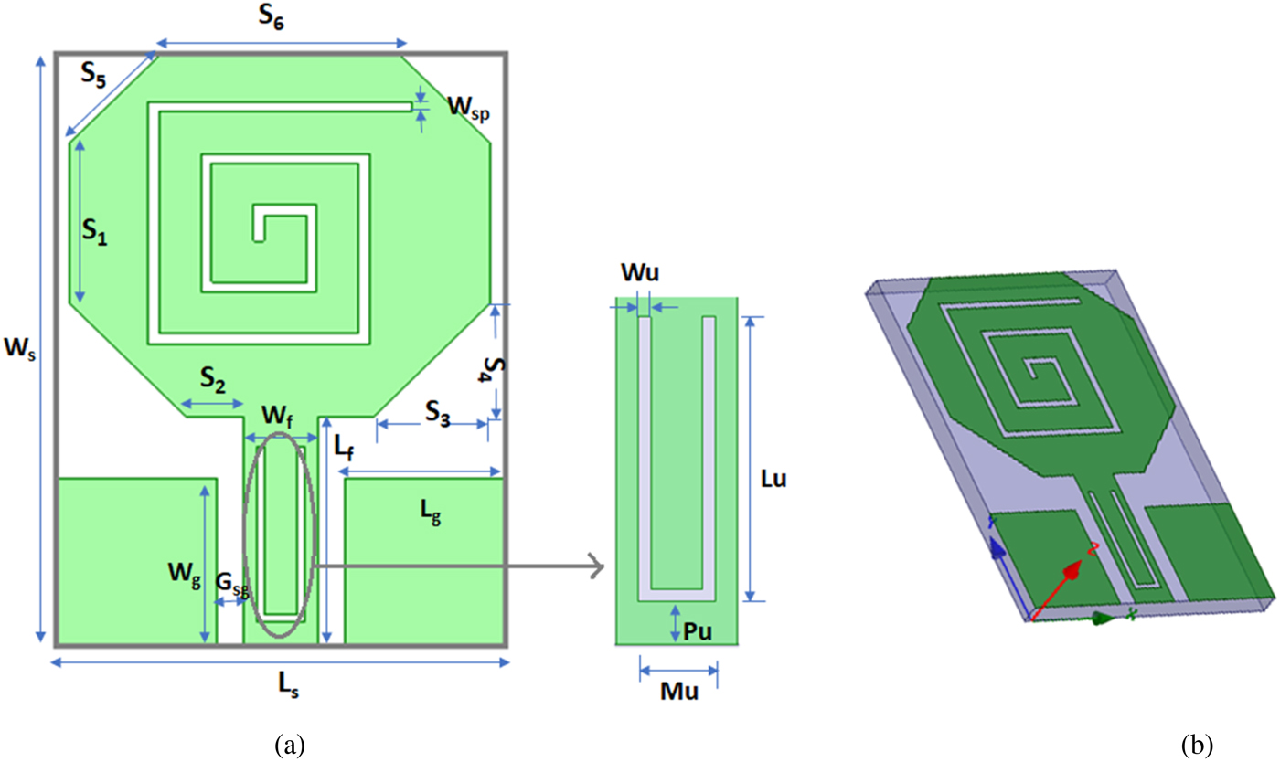
Fig. 1. Design layout of the proposed UWB antenna: (a) top view and (b) 3D view.
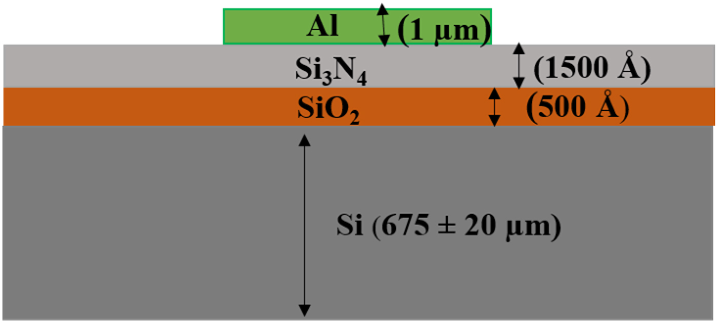
Fig. 2. Layered view of the antenna.
Table 1. Optimized parameter values of the proposed antenna (unit: mm)
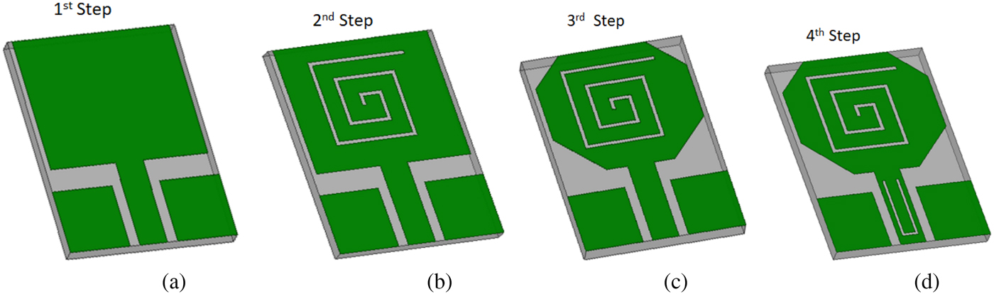
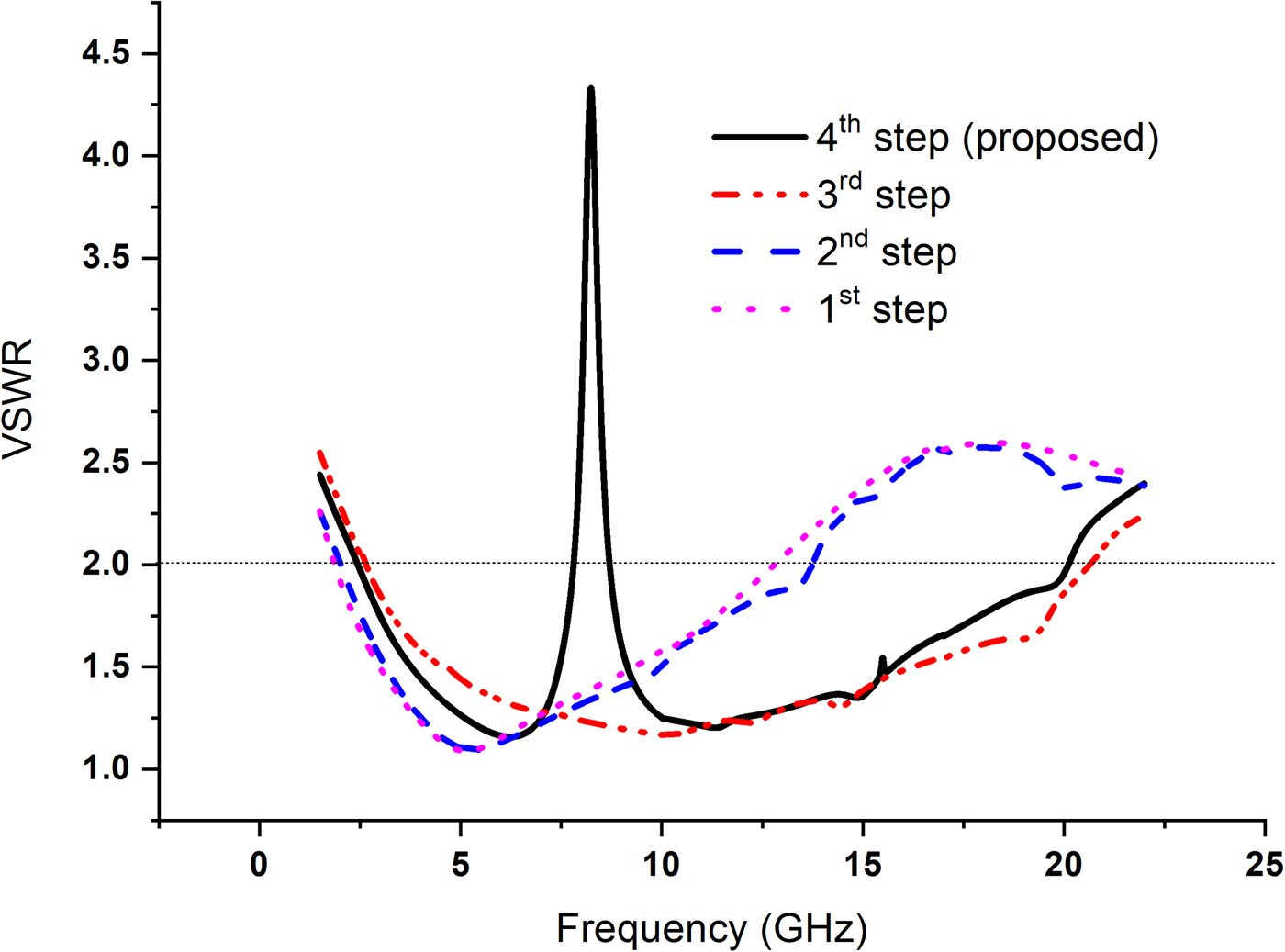
Figure 3 depicts the stepwise modifications as required to realize the proposed structure and the corresponding frequency response characteristics of the respective design steps are shown in Fig. 4. First, a CPW-fed rectangular monopole antenna having a layout area of 8.5 × 11.5 mm2 was taken as a reference antenna (Fig. 3(a)) that operates in the frequency range of 2.43–12.8 GHz. In the second step, a rectangular spiral slot is included within the patch (Fig. 3(b)). Incorporation of the slot within the patch excites higher order modes which overlap with the fundamental mode of the reference patch antenna. This excitation of the higher order modes overlapping with the original bandwidth results in the enhancement of the overall operating bandwidth of the modified design by 1 GHz (operating band 2.45–13.82 GHz). To increase the bandwidth further, four triangular portions are etched out from the four corners (Fig. 3(c)). This corner truncation technique provides increased bandwidth by creating multiple reflections of the surface current from the edged corners. As a consequence, the upper cut-off frequency is shifted to the right-hand side to a great extent. In this step, the bandwidth is enhanced by 6.68 GHz with operating the frequency range of 2.63–20.68 GHz. Finally, in the fourth step, the “U”-shaped slot is incorporated into the feedline (Fig. 3(d)) to achieve band-notch characteristics. The total length of this slot is approximately equals to the half of the guided wavelength (λ g/2) corresponding to the desired center frequency f c = 8.2 GHz which is the mid-frequency of the targeted notched band 7.9–8.4 GHz. This “U”-shaped slot in the feedline acts like a band reject filter by confining most of the surface current within it and allowing a minimal amount of current to flow to the radiating patch. As a result, the antenna remains irresponsive within the frequency range of the targeted notched band.

Fig. 3. Design steps of the proposed antenna: (a) reference antenna, (b) inclusion of spiral slot on patch, (c) etching out from the four corners, and (d) inclusion of “U”-shaped slot in the feedline.

Fig. 4. VSWR characteristics comparison of different design modification steps shown in Figs 3(a)–3(d).
The “U”-shaped slot has a very simple geometry along with four parameters such as arm length (L u), width (W u), separation between two arms of the slot (M u), and distance from the bottom (P u). After a thorough investigation using parametric analysis, it is found that L u and P u are the dominant factors which affect the center frequency (f c) and bandwidth of the notched band respectively. The effect of L u on f c is shown in Fig. 5. It is observed that, with the increment of L u from 2.5 to 3.8 mm, f c decreases from 11.08 to 7.27 GHz.

Fig. 5. Effect of L u on f c of the notched band for the optimum feedline slot parameters such as M u = 0.9 mm, W u = 0.15 mm, and P u = 0.5 mm.
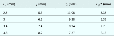
Table 2 shows different values of L u and their corresponding total slot length values L t and as well as simulated f c values. From the geometry of the slot (Fig. 1(a)), L t can be obtained using the following equation:
 $$L_t = 2L_u + M_u-2W_u$$
Table 2. List of the center frequency (f c) of the notched band for different values of L u
Now, for each value of f c, guided wavelength λ g can be calculated using the following formula:
 $$\lambda _g = \displaystyle{{\lambda _0} \over {\sqrt {\varepsilon _{eff}}}} = \displaystyle{c \over {\,f_c\sqrt {\varepsilon _{eff}}}} $$
where c is the speed of light in free space and ε eff is the effective permittivity of the material. For the substrate having a low thickness, ε eff can be calculated using the following approximate formula [Reference Chen, See and Qing30, Reference Abbosh and Bialkowski31]:
 $$\varepsilon _{eff}\approx \displaystyle{{\varepsilon _r + 1} \over 2}$$
where ε r is the relative permittivity of the material.
It is clear from Table 2 that the total slot length should be approximately equal to half of the guided wavelength to obtain the desired center frequency of the notched band. In the proposed antenna, the desired notched band is 7.9–8.4 GHz with the center frequency of 8.2 GHz. Corresponding to the desired center frequency, the optimum value of L u is obtained as 3.4 mm.
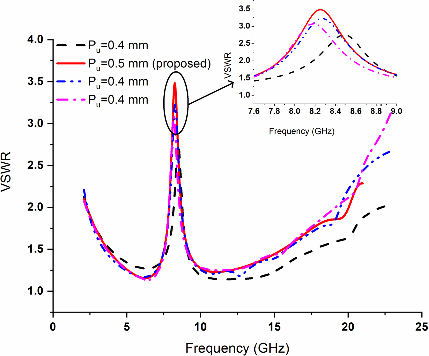
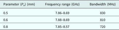
Now keeping L u fixed at its optimum value, bandwidth of the notched band is adjusted by changing P u. Figure 6 shows the effect of P u on the bandwidth of the notched band. It is observed that the increment of P u results in decrement of bandwidth. When P u increases from 0.5 to 0.8 mm, bandwidth decreases from 830 to 720 MHz. It can also be noted that changing P u from its optimum value of 0.5 mm results in decrement of the peak value of rejection ratio. Table 3 lists the obtained notched bandwidth value corresponding to P u.

Fig. 6. Effect of P u on the notched bandwidth with optimum design parameters of the feedline slot such as L u = 3.4 mm, M u = 0.9 mm, and W u = 0.15 mm.
Table 3. Effect of P u on the bandwidth of the notched band

Fabrication process
High resistive, FZ processed silicon wafer (ρ≥8 kΩ-cm, tan δ = 0.01, and ε r = 11.8) with the thickness of 675 ± 20 µm has been chosen as the antenna substrate. The surface of the wafer is oxidized to form a layer of SiO2 having a thickness of 0.05 µm that acts as an insulating membrane. As SiO2 generates some compressive stress on the wafer, another 0.15 µm thin layer of silicon nitride (Si3N4) is deposited above SiO2 to counterbalance that effect. These two layers are used as a buffer layer over the silicon substrate. On the top, 1 µm thick aluminum (Al) layer is deposited by DC magnetron sputtering followed by dry etching of the metal using the mask.
Results and discussion
Characteristics in the frequency domain
This section demonstrates different performance parameters of the proposed structure. Along with the inset image of the fabricated prototype, the measured and simulated resonance characteristics of the proposed antenna are shown in Fig. 7. The graph reveals UWB behavior of the proposed antenna having bandwidth extended up to 20.1 GHz from 2.5 GHz along with band rejection capability ranging from 7.8 to 8.7 GHz. The measurement has been carried out using a R&S®ZVA-40. A good agreement between simulated and measured data is obtained up to 17 GHz. The deviation beyond 17 GHz may be due to the inaccuracies that arise at the time of conductive epoxy spreading at the feed point of the antenna. As this step is performed manually, it often results in asymmetrical spreading of the conductive epoxy. It may also cause changes in the pitch size (separation between signal and ground plane) of the actual CPW line. It further degrades the characteristic impedance of the transmission line, which may be responsible for impedance mismatching at any arbitrary frequency. A standard dicing tool with a diamond cutter is used for dicing purpose, and conductive epoxy (H70E) is used as an adhesive material for integrating the RF connector with the antenna.

Fig. 7. Comparison of simulated and measured VSWR characteristics.
Variation of radiation efficiency with respect to frequency is shown in Fig. 8. It is observed that the radiation efficiency lies in the range of 96 ± 1% over the entire band except at the notched band. It sharply decreases to 62% at f c of the notched band indicating good band-notched characteristic of the proposed antenna.
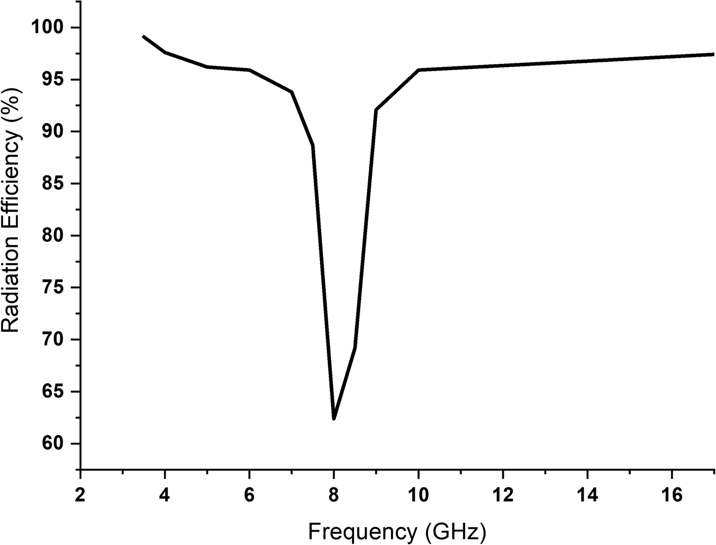
Fig. 8. Plot of radiation efficiency of the proposed antenna with frequency.
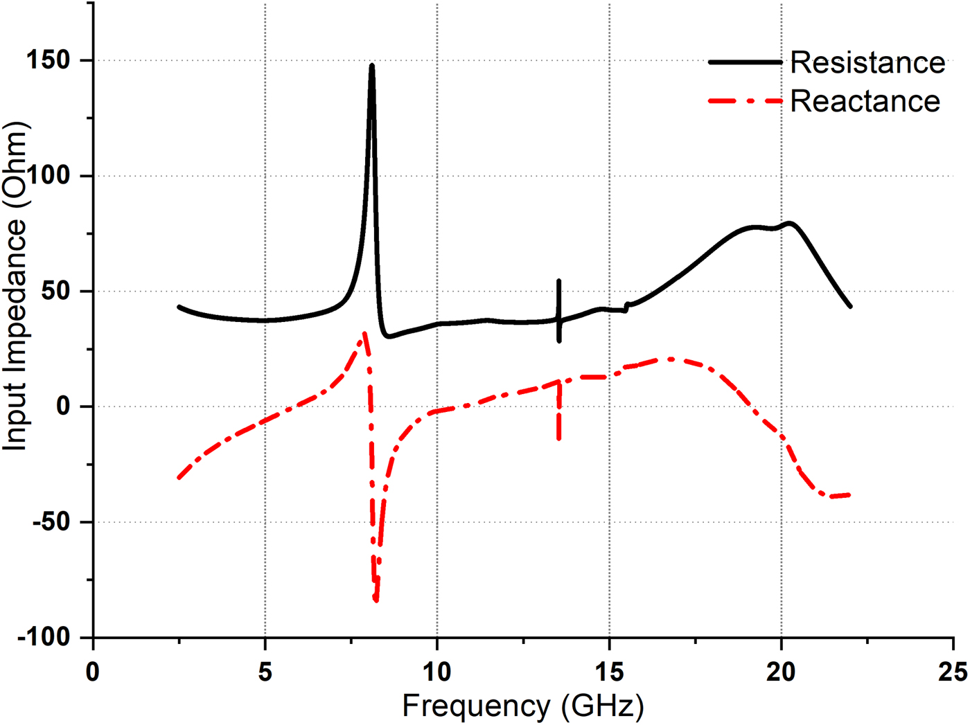
Figure 9 shows the input impedance variation with frequency. It is seen that the real and imaginary parts of the input impedance oscillate around 50 and 0 Ω, respectively, over the entire operating bandwidth except in the notched region. At the center frequency of the notched band, i.e. 8.2 GHz, the real part of the input impedance reaches 148 Ω, and the imaginary part exhibits parallel resonance characteristics at that frequency.

Fig. 9. Variation of real and imaginary parts of the input impedance with frequency.
Figure 10 depicts surface current distributions at 8.2 and 12 GHz. At 8.2 GHz, the current is only concentrated within the “U”-shaped slot in the feedline. The current doesn't reach the radiating patch at all. Therefore, the antenna remains irresponsive at that frequency. At 12 GHz, lying outside the notched band, the current distribution is more at the lower edge of the radiating patch and around the rectangular spiral slot.
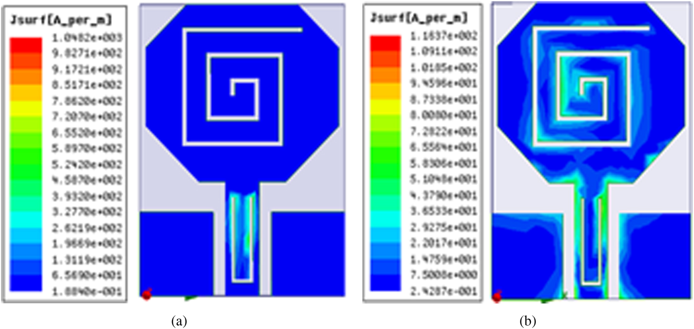
Fig. 10. Current distribution of the designed antenna at center frequency of the notched band and outside the notched band frequency: (a) at f = f c = 8.2 GHz and (b) at f = 12 GHz > f c.
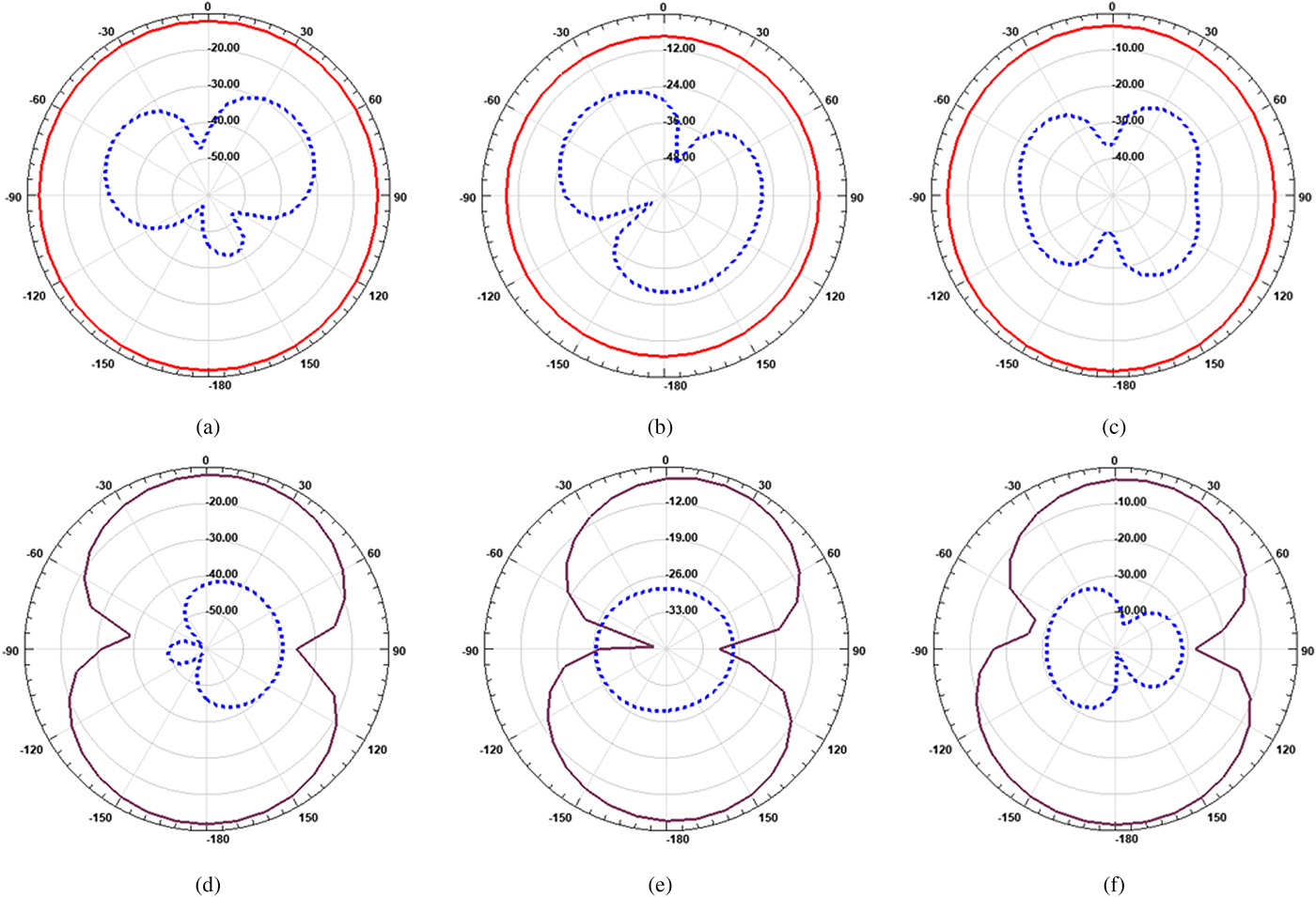
Figure 11 depicts the simulated far-field radiation pattern of the proposed antenna in the XZ (H-plane) and YZ planes (E-plane) at 8.24, 10, and 16 GHz. The plot indicates that the antenna exhibits an omnidirectional pattern in the H-plane and in the E-plane, it looks like conventional monopole like pattern. In Fig. 11, it is also observed that there is good isolation between co- and cross-polar levels throughout the entire operating band.

Fig. 11. Simulated H-plane and E-plane radiation patterns at different frequencies. For H-plane at (a) 8.24 GHz, (b) 10 GHz, and (c) 16 GHz; and for E-plane at (d) 8.24 GHz, (e) 10 GHz, and (f) 16 GHz.
Characteristics in the time domain
The essential parameters of UWB antenna in the time domain are the transfer coefficient |S 21| and group delay (τ g). The group delay can be expressed using the following equation:
 $$\tau _g = -\displaystyle{{\partial \varphi} \over {2\pi \partial f}}$$
where φ is the phase of the antenna in the far field region and f is the frequency.
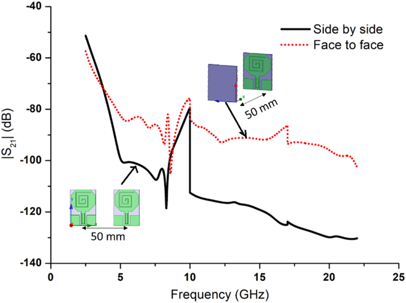
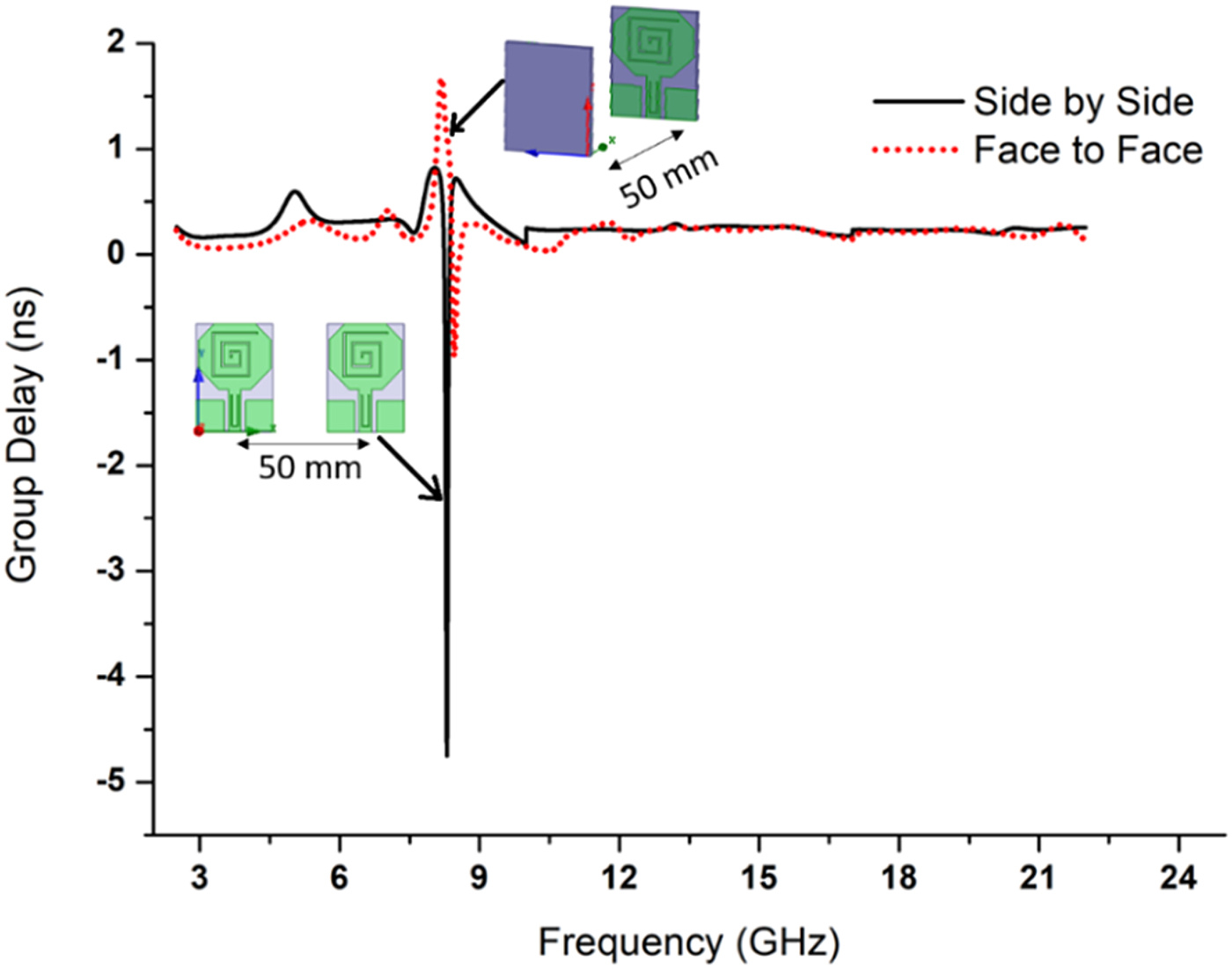
Two identical antennas must have to be placed in their far-field region to calculate these two parameters. In this regard, they are positioned here 50 mm apart from each other in both side by side and face to face configurations. Simulated |S 21| and group delay are depicted in Fig. 12 and Fig. 13, respectively. It is observed in Fig. 13 that the group delay is almost constant (variation is <1 and 0.5 ns for the side by side and face to face arrangements, respectively) over the entire operating bandwidth except in the notched region. Constant group delay indicates linear variation of the phase with frequency. This criterion, i.e. linear variation of phase with frequency offers distortion-less transmission of pulses by the antenna, and that is the most attractive feature of the proposed UWB antenna.

Fig. 12. |S 21| characteristics of the proposed antenna for side by side and face to face arrangements.

Fig. 13. Group delay variation of the proposed antenna for side by side and face to face arrangements.
Conclusion
This paper has demonstrated the detailed design and development of a compact on-chip monopole antenna having fractional bandwidth of 156% which covers UWB (3.1–10.6 GHz), Ku band (12–18 GHz), and some portion of K band (18–26.5 GHz). This antenna has an integrated band-notch filtering capability to avoid interference with the 7.9–8.4 GHz band which is assigned for X-band uplink satellite communication systems. Compact design (8.5 × 11.5 mm2) is the main attractive feature of this research work. The proposed antenna can be used for short-range, high-speed communication. The fabrication process is simple and compatible with the standard CMOS process. Implementation of the antenna on silicon makes it a suitable candidate for future SoC application.
Author ORCIDs
S. Mandal, 0000-0003-3215-2538.
Acknowledgement
The authors gracefully acknowledge financial support provided by Visvesvaraya Ph.D. scheme, Ministry of Communications and Information Technology, Govt. of India, Grant No. Ph.D.-MLA/4(29)/2015-16/01 and Special Manpower Development Programme for Chips-to-System Design (SMDP-C2SD) under Govt. of India, Grant No. 9(1)/2014-MDD (Vol III). The authors are also thankful to Semi-Conductor Laboratory (SCL), Chandigarh for providing fabrication and measurement facility.
 Sanjukta Mandal received her B.Tech degree in Electronics & Instrumentation Engineering and M.Tech degree in Electronics & Communication Engineering from the University of Kalyani in 2012 and 2014, respectively. Her master's thesis was on frequency selective surface (FSS). She worked as a Project Fellow in the project entitled “Design of Mobile Robot Technology for Security, Surveillance, Mining, Building Inspection and Planetary Exploration (ESC0112/RP-1)” in CSIR-CMERI, Durgapur, West Bengal, India. She is currently pursuing her Ph.D. from the National Institute of Technology, Durgapur, West Bengal, India. Her current research interests include on-chip antenna design for short range communication and gain enhancement of on-chip antennas.
 Ayan Karmakar received his B.Tech degree in Electronics and Communication from Maulana Abul Kalam Azad University of Technology, West Bengal (formerly known as WBUT) in 2005. Thereafter, he joined ISRO as a “Scientist” and subsequently posted to Semi-Conductor Laboratory (SCL), Chandigarh in Advanced Micro & Nano System Division. His research interests include design and development of L, S, C, X, and K-band passive microwave integrated circuits and antennas using silicon-based MIC and RF-MEMS technology. His fields of expertise are expanded in fabrication technology of various MEMS-based sensors and their testing strategies too. He completed his M.Tech from NIT-Durgapur with the specialization in Telecommunication. He serves as a reviewer for EJAET (European Journal of Advanced Engineering and Technology). He is the life member of IETE, India.
 Harsh Vardhan Singh received his B.E. degree in Electronics & Communication Engineering from Rajiv Gandhi Proudyogiki Vishwavidyalaya, Bhopal in 2010. He received his M.Tech degree in Telecommunication Engineering from the National Institute of Technology Durgapur (NITD) in 2014. His master's work was on the reduction of SLLs and SBLs of time-modulated antenna arrays using various optimization algorithms. He is currently pursuing his Ph.D. degree at the NITD since 2015. His topic of research is the design of on-chip antennas for RF-telemetry applications. His research interest includes on-chip antennas, chip inductors, antenna arrays, and RF circuits for wireless communications.
 Sujit Kumar Mandal received his B.Sc. degree in Physics Honours from the University of Calcutta in 2001. He completed his B.Tech and M.Tech in Radio Physics & Electronics from the Institute of Radio Physics & Electronics, C. U. in 2004 and 2006, respectively. He received his Ph.D. degree from the National Institute of Technology, Durgapur where he is presently working as an Assistant Professor in the Department of Electronics and Communication Engineering. His present research area includes application of soft computing techniques in antenna array optimization, time-modulated antenna arrays, microstrip patch antennas, RF-energy harvesting, and on-chip antenna design. Dr. Mandal is a member of IEEE.
 Rajat Mahapatra was born in Kolkata, India in 1972. He received his M.Tech. and Ph.D. degrees from the Indian Institute of Technology (IIT) Kharagpur, India in 1999 and 2005, respectively. During 2005–2010, he was a Research Associate with the School of Electrical, Electronics and Communication Engineering, Newcastle University, Newcastle upon Tyne, UK. He is currently an Associate Professor with the Department of Electronics and Communication Engineering, National Institute of Technology (NIT), Durgapur, India. He has published about 80 articles in referred international journals and conference proceedings. His areas of interest include physics, technology and characterization of MOS devices, memory, and sensors.
 Ashis Kumar Mal received his bachelors' degree in Electronics and (Tele)Communications Engineering from Bengal Engineering College (now IIEST) Shibpur and Masters' from IIT Kanpur in 1989 and 1994, respectively. He obtained his Ph.D. from IIT Kharagpur in 2009 in the field of Microelectronics and VLSI. He has about 25 years of teaching experience and currently with NIT Durgapur as an Associate Professor serving the Department of Electronics & Communication Engineering. He has published more than 60 articles in refereed international journals and conferences. He is an IEEE Solid-State Circuits Society (SSCS) member. His interest includes Analog/Mixed Signal VLSI (AMS) and digital-assisted analog (DAA).