I. INTRODUCTION
Millimeter-wave (mm-wave) applications demand for complex integrated circuit, well beyond the capabilities of today's microwave MMIC technologies. CMOS/BiCMOS-based mm-wave MMICs have achieved impressive results well beyond 100 GHz, but with low-power capabilities and aggressive scaling. Compound semiconductor technologies, such as InP technologies, exhibit higher breakdown voltages and higher frequency performance capabilities with relatively relaxed scaling. Thus, InP technology offers better power capabilities and higher breakdown voltage at similar maximum frequency of oscillation (fmax) values and enables access to even higher frequencies as compared to BiCMOS with similar technological dimensions. In order to achieve high output power levels at mm-wave frequencies and beyond with low-noise properties and complex integrated circuit, it would be desirable to merge these two separate technologies.
With this background as a motivation, work on hetero-integration of different semiconductor technologies with complementary functionality is picking up speed. Most notably, research in InP-on-BiCMOS within a DARPA-funded consortium has to be mentioned (see, e.g. [Reference Raman, Chang, Dohrman and Rosker1, Reference Kazior2]), but also activities on combining GaN-on-Si CMOS are ongoing [Reference Hoke3]. Driven by automotive applications and high-speed back-haul links, a lot of experience has been accumulated with BiCMOS circuits in the E-band [Reference Nicolson4, Reference Sarkas, Nicolson, Tomkins, Laskin, Chevalier, Sautreuil and Voinigescu5], whereas InP HEMT and DHBT technologies have been applied widely in high-speed communications, such as 100 G fiber communications [Reference Sano, Fukuyama, Nakamura, Mutoh, Nosaka and Murata6] or mm-wave wireless communications [Reference Kozhuharov, Bao, Gavell and Zirath7, Reference Takahashi, Hirata, Takeuchi, Kukutsu, Kosugi and Murata8].
In this work, we demonstrate the unique capabilities, which can be achieved with hetero-integrated InP-on-BiCMOS mm-wave MMIC. Special emphasis is given to signal sources, due to the lack of powerful low-noise signal sources at frequencies beyond 100 GHz. An important aspect in the development of the wafer-level hetero-integrated process is the implementation of low-loss transitions from one technology to the other, capable of operation well beyond 100 GHz. All circuits discussed here employ dedicated transitions with low-loss performance up to 200 GHz, as discussed below. A number of various combined circuits have been realized, such as frequency multipliers in InP driven by BiCMOS voltage-controlled oscillator (VCO) sources. In particular, this paper describes in detail a 164 GHz signal source that employs an 82 GHz fundamental frequency VCO in BiCMOS to drive a frequency doubler and amplifier chain in a transferred-substrate (TS) InP-DHBT technology [Reference Kraemer, Rudolph, Schmueckle, Wuerfl and Traenkle9]. An additional circuit presented in this paper operates at 96 GHz with higher output power levels. Both technologies are integrated using a wafer-level hetero-integration benzocyclobutene (BCB) bonding process. This approach is a joint effort of the two Leibniz research institutes FBH and IHP and will pave the way toward additional applications such as high-resolution and highly directive radars, imaging, or high-speed communications in the lower THz range. It is shown that changing the carrier substrate for the TS-InP process from the usual AlN to a BiCMOS substrate does not greatly influence the power-handling properties of InP-DHBT MMIC circuits, which remain also unaffected by the BiCMOS structures underneath, for example, fillers, lines, etc.
The following sections of the paper describe the combined InP-on-BiCMOS circuit as well as the individual circuit components in the BiCMOS and TS-InP technologies. A demonstration of the performance of the crucial interconnections to 200 GHz is provided. The fact that replacing the AlN substrate with a BiCMOS substrate does not degrade InP-DHBT power performance is shown with a 96 GHz doubler circuit and finally it is demonstrated that InP-DHBT circuit performance is essentially unchanged regardless of the substrate being employed.
II. OVERALL CONCEPT
All hetero-integrated MMICs are based on signal sources in BiCMOS followed by an InP MMIC with on-chip transitions between the two blocks. As an example, a block diagram of the hetero-integrated 164 GHz MMIC signal source is shown in Fig. 1. The hetero-integration technology has been described in [Reference Krämer10, Reference Ostermay11] in full detail. Here, we will describe only the most important steps. The process starts with a fully standard BiCMOS processing. After finalizing the BiCMOS processing up to the top metals, a planarization step is introduced, which provides a surface with a topography of <100 nm across the wafer. The BiCMOS wafers are then cut-out into several 3″ wafers. Independently, the transfer-substrate InP process is performed with scaled dimensions, which are determined by the mismatch between the thermal expansion coefficients. This means that the InP circuits are pre-scaled such that at around 200°C both the BiCMOS and the InP MMIC have exactly the same dimensions. Subsequently, both wafers are assembled using a BCB-bonding step. All transitions are formed in that bond process on wafer-level with an alignment accuracy of <6 µm across the wafer. The semiconductor hetero-integration technology employed consist of a SiGe-BiCMOS process (SG25H1) in a high-performance 0.25 µm technology with npn-HBTs up to f T/f max = 180/220 GHz and a TS-InP-DHBT technology with f T/f max values of 350/350 GHz (for a one-finger HBT with an emitter area of 0.8 × 5 µm2). A detailed description of this process is beyond the scope of this paper, but can be found in [Reference Ostermay12, Reference Ostermay11].

Fig. 1. Block diagram of hetero-integrated 164 GHz MMIC signal source; right-hand pads indicate the single-ended RF output, DC pads can be seen above and below the circuit. Green area is SiGe BiCMOS only and yellow area denotes InP-on-BiCMOS.
In Fig. 1, an 82 GHz VCO is realized in BiCMOS, followed by a frequency doubler–amplifier chain using the TS-InP-DHBT process on top of the already manufactured BiCMOS circuits.
Stacking InP circuits on top of the BiCMOS structure will inevitably result in a detuning of the BiCMOS circuits, in our case primarily the VCO's resonant frequency. This effect is small since signals in the BiCMOS structures remain within the CMOS dielectric stack and do not interact with metallization in InP because the ground (Gd) InP layer is connected to SiGe ground layer. The main detuning effect is the low permittivity BCB (ε r = 2.65) on top of the BiCMOS elements, which can be fully eliminated if one takes into consideration the BCB stack already during BiCMOS circuit design.
In order to ensure first pass design, it was decided to place the BiCMOS and InP circuit parts offset from each other, so that the risk of undesired interference is minimized. A full three-dimensional integration approach will be explored in forthcoming runs with a stack of MMICs in both technologies directly on top of each other, providing considerably more compact circuits. Undesired coupling between circuit elements will also be investigated, because of its potential to trigger instabilities within the MMIC.
In the micrograph in Fig. 2, the complete circuit is shown. The VCO tank circuit can be seen on the left, in the center the BiCMOS–InP via interconnect, and the TS-InP circuit on the right. Interconnects can be placed everywhere in the circuit and daisy chain with transitions from InP to SiGe and back to InP circuits have been already explored. The combined circuit size is 1 × 3 mm2 and the InP part covers 1 × 1.77 mm2. The BiCMOS circuit becomes visible because in the InP part all elements and metallization patterns are blanked out and hence only the transparent BCB layer remains in this area.
Fig. 2. Micrograph of the 164 GHz hetero-integrated source; the VCO structure is visible on the left and RF output pads can be seen on the right.
III. THE LOW-LOSS BICMOS TO INP TRANSITIONS
Low-loss transitions between the BiCMOS and InP circuit parts are of paramount importance for the hetero-integrated circuits. Transitions have to be optimized in terms of size and RF loss. The transitions employed here have a diameter of 10 µm, but 5 µm vias have also been successfully realized. Due to the miniaturized structures and thanks to optimization using electromagnetic simulations, a return loss better than 12 dB from DC to beyond 200 GHz and an insertion loss below 0.4 dB up to 100 GHz and below 1 dB up to 220 GHz is achieved [Reference Ostermay12–Reference Krozer14]. The reliability of such a transition can be verified with a chain of transitions, where misalignment and connection errors will cascade if there is a problem with the bonding process and/or the electromagnetic optimization.
A test structure of cascaded transitions from microstrip lines on InP to those on BiCMOS and vice versa is shown in Fig. 3. It consists of a total of ten transitions alternating between top metal on the InP layer and top metal on the BiCMOS layer. Its insertion and return loss was measured up to 110 GHz.
Fig. 3. Test structures with transitions between the top InP microstrip layer and the top metal layer in the BiCMOS process. The vias next to the InP microstrip line ensure that a common ground is shared between the InP and BiCMOS circuit parts.
It can be observed in Fig. 3 that the signal via is not perfectly in the centre of the via catch pad, but it is sufficiently accurate to achieve good high-frequency behavior. S-parameters measured on-wafer from 50 MHz to 110 GHz are plotted in Fig. 4 for the structure in Fig. 3. The figure shows the insertion loss and reflection coefficients for six samples across the wafer overlaid. Dividing by the number of transitions, assuming that the line losses are negligible, and noting that the return loss is better than 10 dB to beyond 110 GHz, we can estimate a loss of <0.35 dB/transition at 100 GHz and <0.5 dB/transition at 200 GHz.
Fig. 4. Transmission (left) and reflection (right) properties of six identical multi-transition structures measured on the same wafer to 110 GHz.
The results are very encouraging and demonstrate that a reliable connection can be established between the BiCMOS and InP circuit layers with low loss and without placement restrictions within the circuit. The uniform response from multiple identical structures measured across the wafer demonstrates high reproducibility of the interconnection.
DC biasing of the BiCMOS VCO and buffer as well as the three TS-InP-DHBTs is all done through DC pads on the top InP metallization layer. A continuous ground plane is located between the InP circuit area and the BiCMOS wafer. This ensures a low-loss thin-film microstrip wiring environment in the InP part, without interaction with the SiGe BiCMOS circuitry and prevents higher losses associated with the silicon substrate below. An exception to this is the area beneath the series capacitors in the high-frequency signal path, where an opening in the ground plane is made to reduce the parasitic capacitance between the ground plane and the lower capacitor plate.
It was not well established prior to the run if the fillers in the SiGe process will affect the performance of the InP circuit in the areas, where the ground is open. This has been investigated on individual devices together with possibilities for integrated thermal heat sinks in SiGe.
IV. DEVICE RF PERFORMANCE
The performance of InP-DHBT devices on top of the SiGe BiCMOS stack has been compared to that of the original TS-InP-DHBT process. Small-signal and large-signal operations have been investigated. Figure 5 illustrates a comparison of the TS-InP-DHBT and of the InP-on-BiCMOS InP-DHBT operation with the device model available at FBH. The device model accurately represents measured results for a single-finger transistor, whereas it is slightly optimistic for a double-finger device. Large-signal performance measured for different shots across the wafer are also provided in Fig. 5(b), which demonstrates rather good uniformity. The results indicate that high-output powers can be obtained from both processes and the hetero-integration InP-on-BiCMOS process does not deteriorate significantly the performance of the active devices.
Fig. 5. Large-signal performance of single-finger DHBT in TS process at 77 GHz (a) and double-finger DHBT in InP-on-BiCMOS process at 96 GHz (b). Dots represent simulations, solid lines are measurements.
Small-signal measurements have also been performed to investigate the impact of fillers in SiGe and thermal heat sinks in SiGe for the top InP circuits on active device performance. Figure 6 shows small-signal measurement comparison between the original and the hetero-integrated S11 and S22. From Fig. 6, it can be concluded that there is only a minor impact by the fillers in SiGe on InP HBT performance. This is most probably due to the fact that the filler structures are small and non-interconnected. Also a structure underneath the InP-DHBT transistor structures, which is connects the Si substrate with the top metal in SiGe does not impact small-signal performance and provides a heat-sink for the dissipated power in the transistor.
Fig. 6. Small-signal performance of single-finger DHBT in TS process and the same device with fillers in the InP-on-BiCMOS process (a) and implementing a heat-sink underneath the transistor in SiGe (b). Measurements are in the range 1–110 GHz. Cyan and blue lines are results for the standard TS process, red and magenta are results for InP HBT transistors in InP-on-BiCMOS process. Insets show the transistor layout for the two cases, respectively.
V. MMIC CIRCUIT DESIGN
A) BiCMOS circuit
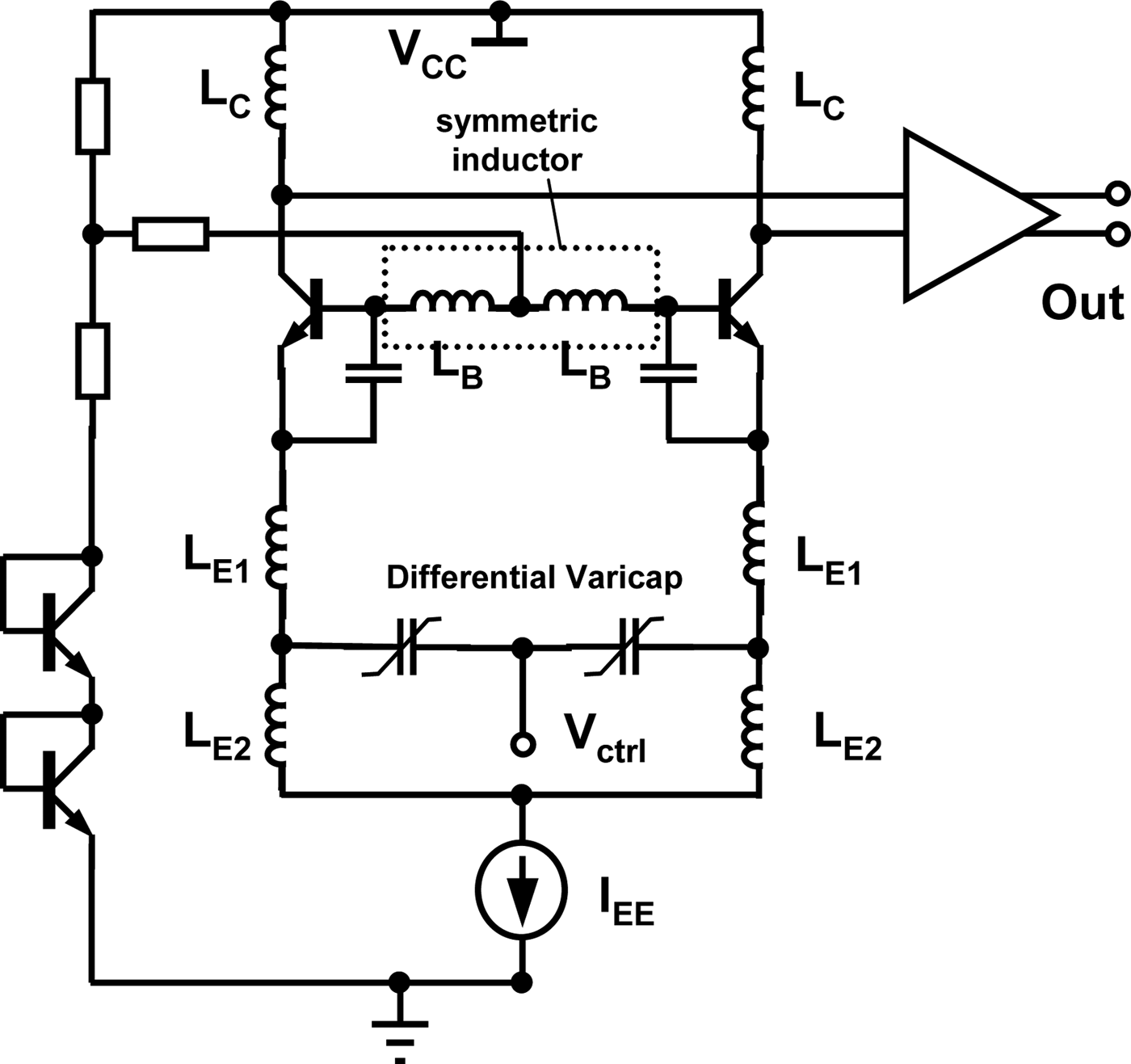
The oscillator features a differential Colpitts topology, which has been a common choice in mm-range VCOs for low-phase noise applications. Its simplified schematic in Fig. 7 shows a modified differential Colpitts topology with inductance LE2 in parallel, and inductance LE1 in series to the varactor. Adding LE1 and LE2 reduces oscillator phase noise by increasing the loaded quality factor of the resonant circuit compared to the case of a pure varactor.
Fig. 7. Simplified schematic of the differential Colpitts VCO and output buffer.
From the Leeson formula, it is clear that we have to increase Q-factor of the tank and voltage swing in the tank to minimize the oscillator phase noise. In the mm-wave range Q-factor is primarily limited by the varactor. A differential MOS varactor with lower resistance was used. It exhibits two MOS varactors, which are connected directly in silicon. This silicon connection has small resistivity because the varactors are just 0.3 µm apart. This structure avoids contacts from N-well to Metal1 reducing varactor resistance, and hence increasing the varactor Q. There is an additional contact to the N-well for hole extraction, which are generated at negative gate voltages.
Inductances, shown in the schematic, are realized in layout by transmission lines. The top metal layer, with a thickness of 3 µm, is used for the signal line. It is 9 µm above the bottom metal layer, which forms the ground plane.
The VCO is followed by a single-stage buffer that features cascode topology. The buffer is inserted to provide isolation between the VCO core and the rest of the circuit. For this purpose, the cascode topology provides good isolation and matching.
B) TS-InP-DHBT circuit
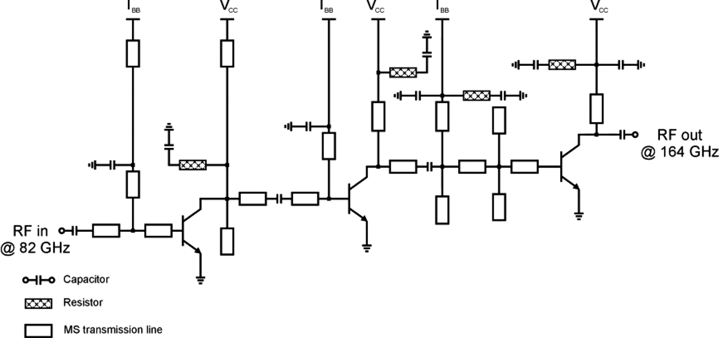
The TS-InP-DHBT part of the circuit consists of a 164 GHz doubler and a two-stage amplifier. The schematic circuit is shown in Fig. 8. All three stages use the same two-finger HBT with an emitter size of 0.8 × 5 µm2. Biasing for each TS-InP-DHBT stage can be independently controlled for optimum bias point adjustment. This is mostly a concern for the doubler stage, which operates under large-signal conditions. The expected power of the second harmonic is at a level where the subsequent amplifying stages have to be optimized for highest gain.
Fig. 8. Three stage InP doubler–amplifier chain; the first stage is the doubler. Each stage operates with a collector voltage of 1.5 V and a collector current of ~20 mA for the given results, but independent bias of each stage is possible.
Simulated results of the cascaded doubler–amplifier chain are used in the following discussion to explain the design methodology and understanding the single-ended measured results. The characterization of the circuit can be performed only in conjunction with the BiCMOS VCO.
The doubler employs a single-ended topology with the input matched to the VCO target frequency of 85 GHz and the output to the second harmonic.
In order to suppress the fundamental frequency, a notch filter is implemented, which consists of an open-circuited stub with a radial stub at the end to reduce the length needed to suppress the fundamental frequency. The filter is narrow band, but provides good attenuation of the third harmonic as well. The total suppression of the fundamental frequency in the doubler–amplifier chain is 12 dB at the center frequency. An amplifier with two cascaded common-emitter HBTs is boosting the power of the second harmonic to the milliwatt level. According to simulations, the input return loss is expected to be better than 10 dB in the 77–115 GHz frequency range and the output return loss better than 10 dB in the 141–193 GHz range. The simulated S-parameters for the TS-InP-DHBT doubler–amplifier chain are plotted in Fig. 9.
Fig. 9. Simulated S-parameters of the TS InP doubler–amplifier chain.
The actual VCO frequency was 82 GHz instead of the expected 85 GHz. This does not significantly affect interstage matching in the circuit of Fig. 8, because simulated input and output return loss have good broadband properties, with ~13 and 14 dB, at 82 and 164 GHz, respectively. But, the effect of the notch filter is unfortunately greatly reduced, which can be seen from the S 21 curve in Fig. 9. The suppression of the fundamental frequency is only 0 dB due to the frequency shift, which might adversely affect the amplifying stages. But it is not influencing the power meter reading due to the use of probe waveguides with cut-off frequencies above the fundamental frequency as explained in the measurement section. The graph in Fig. 10 presents simulated conversion gain and output power of the first and second harmonic based on the actual fundamental frequency of 82 GHz. The output power of the undesired first harmonic is quite constant at 2 dBm for the input power range from 0 to 10 dBm. For an expected VCO power of 6–8 dBm, the second harmonic output power is simulated to be around 2 dBm. Simulated conversion loss for the doubler alone is 11 dB, but the two-stage amplifier is expected to provide ~6 dB gain at 164 GHz.
Fig. 10. Simulated conversion gain (CG) and output power of the first and second harmonic for the doubler–amplifier chain. Assumed fundamental frequency is 82 GHz. Actual input power was measured to be about 8 dBm.
C) Measurements on the 164 GHz MMIC signal source
The circuit is probed on-wafer with a G-band probe with a pitch of 75 µm and connected to a WR05 waveguide. A WR05–WR10 waveguide taper provides a transition to the input of an Ericson PM4 power meter. The loss from probe-tip to power sensor is estimated to be 3 dB using an on-wafer standard. The cut-off frequency of the WR05 waveguide is 112 GHz, which ensures that no power from the fundamental frequency is registered in the power measurement. The power level of the third harmonic is approximately 20 dB lower than the second harmonic according to simulations and should thus have a negligible influence on the measurement. The measured output power is 0 dBm, which is not far from the expected value simulated in Fig. 10.
A second version of the circuit featuring a simple microstrip through-line replacing the doubler–amplifier chain was also available on the wafer and enabled direct measurement of the VCO spectrum and power. The results are plotted in Fig. 11, the spectrum was measured with an external W-band down-conversion mixer exhibiting a conversion loss of approximately 35–40 dB. De-embedding this, one obtains for the VCO only circuit an output power of 4.8 dBm, measured using an Agilent W8486A W-band power sensor connected with a WR10 waveguide to the RF probe. A tunable frequency range of 81.8–82.4 GHz for the VCO could be determined with less than 0.2 dB variation in the output power.
Fig. 11. 82 GHz VCO output spectrum measured on the InP-on-BiCMOS wafer.
This is the first circuit of its kind in this frequency range, which makes benchmarking difficult. However, in [Reference Kozhuharov, Bao, Gavell and Zirath7] a source is described based on a pure InP-HBT G-band VCO plus a doubler/quadrupler, which achieves −2 dBm in the 113–118 GHz band and −4 dBm in the 212–228 GHz band. The present realization with 0 dBm at 164 GHz compares well with this data.
D) Hetero-integrated InP-DHBT 96-GHz doubler and amplifier
As described above, the active InP-HBT device performance has not deteriorated when hetero-integrated with SiGe BiCMOS. This has also been tested on the MMIC level. A 96-GHz doubler with and without power MMIC amplifier was implemented in InP-DHBT process on top of the SiGe BiCMOS. This was done in order to verify whether the power capabilities of TS-InP circuits would be compromised using a silicon substrate having a lower thermal conductivity than, e.g. AlN.
The doubler is a single-ended design, see Fig. 12, with the same basic methodology as used for the 164-GHz doubler.
Fig. 12. Single-ended 96 GHz doubler–amplifier in InP with silicon substrate. Notice that the mandatory fillers in the silicon part are removed around parts of the InP circuit where openings in the ground plane occur.
The measured on-wafer small-signal S-parameters of the doubler–amplifier can be seen in Fig. 13.
Fig. 13. Measured S-parameters of the 96 GHz doubler–amplifier circuit.
The suppression of the fundamental frequency with the notch filter is clearly visible from S 21. The output is well matched over most of W-band. The input, however, is matched less well, with a return loss of ~8 dB.
The circuit uses the same two-finger HBT as in the 164-GHz doubler circuit. Optimum conversion gain is 8.3 dB with an output power of 9 dBm at 96 GHz. The saturated output power is 12.6 dBm with a conversion loss of 5.9 dB. The DC power consumption is 90 mW for the optimum conversion gain case and 115 mW under saturated operation for the combined two stages. The P IN–P OUT and conversion gain curves versus input power, for a constant bias point, can be seen in Fig. 14. In the same figure, the P IN–P OUT and conversion gain is also plotted (see dotted curve) for the doubler part only, which has been measured independently. The figure demonstrates the improved gain, ~4 dB, when the doubler is operated in saturation, and the output power performance of the combined circuit versus the doubler alone.
Fig. 14. P IN–P OUT and conversion gain for the 96 GHz doubler–amplifier (solid lines) and doubler only (dots). Best conversion gain is achieved with an input power of 0 dBm, yielding an output power of 9 dBm.
Figure 15 shows the S-parameters of two 96 GHz doublers with practically identical circuit layout, again using a single-ended doubler design based on two-finger HBTs. One doubler circuit is using the standard AlN substrate; the other is using the BiCMOS silicon substrate. The only difference in the layout is that the InP-on-BiCMOS circuit is biased through bias tees and the InP-on-AlN is biased using separate DC pads. The circuits were biased at rather high DC current densities, ~3.7 mA/µm2, but there is no obvious degradation due to the use of the BiCMOS substrate with lower thermal conductivity.
Fig. 15. S-parameters of 96 GHz doublers with similar circuit topology, one with BiCMOS substrate (solid line) and one with AlN substrate (dashed line).
VI. CONCLUSION
This paper demonstrates successful implementation of mm-wave MMICs using a new hetero-integration InP-on-BiCMOS technology. To the authors' knowledge, the paper also shows the first ever published BiCMOS/InP hetero-integrated MMIC in W-band and above. We prove that wafer-level integration of TS-InP and BiCMOS circuits is possible without degrading circuit performance. We also clearly demonstrate the overall benefits in performance outreaching the limits of each individual technology.
The circuit design was performed without any modifications to the transistor models accounting for the stacked approach, so the agreement between measurements and simulations also documents that the hetero-integration does not diminish circuit behavior. Direct comparison of similar circuits using either AlN or silicon substrates show that there is no fundamental change in performance. Reproducible, low loss, and broadband interconnects up to 200 GHz are now available for the demonstrated InP-on-BiCMOS technology to accommodate signal routing between both material systems using complex transmission line circuitry, which is no longer a limiting factor.
ACKNOWLEDGEMENTS
The authors would like to acknowledge partial financial support by the Leibniz Association through the SAW project “HiTeK” and by the DLR under the project “mmRadar4Space”.
Thomas Jensen received M.Sc. and Ph.D. degrees from the Technical University of Denmark in 2005 and 2010. He has been involved in radiometer instrument design, vital signs radar, and THz imaging systems. At the Ferdinand-Braun-Institute in Berlin, he has worked on non-linear circuit design in InP technology and on-wafer measurements at sub-THz frequencies. Currently, he is engaged in design, construction, and operation of instruments for microwave plasma diagnostics in fusion energy research with the physics institute at the Technical University of Denmark.
Thualfiqar Al-Sawaf received the B.Sc. degree in Electrical Engineering at Al-Mustansiriya University and the M.Sc. degree from the University of Kassel in 2006 and 2010, respectively. Since 2010, he is responsible for the design and characterization of millimeter-wave power amplifiers and frequency multipliers for Terahertz applications at the Ferdinand-Braun-Institut (FBH), Germany.
 Marco Lisker received the Ph.D. degree from Otto-von-Guericke University, Magdeburg, Germany, in 2001. He has been a Process Engineer and a Research Staff Member of IHP, Frankfurt/Oder, since 2009.
 Srdjan Glisic received his B.Sc. degree in Electrical Engineering from the Faculty of Electronic Engineering, Nis, Serbia in 2000 and Ph.D. degree from Brandenburgische Technische Universität Cottbus, Germany, in 2010. He joined Circuit Design Department of IHP, Frankfurt Oder, Germany in 2003. He was involved in projects on 60 GHz wireless communication and automotive radar in 77 GHz frequency range. He worked mainly on VCOs, PLLs, PAs as well as PCB design, and system integration. Since July 2013, he works for Silicon Radar GmbH, Frankfurt Oder, Germany. He works on FMCW and pulse radar MMICs.
Mohamed Elkhouly received his B. Sc. and M. Sc. both in Electronics and Communication Engineering from Ain Shams University, Cairo, Egypt in 2003 and 2008, respectively. In 2008, he joined IHP as a researcher in the microwave and millimeter-wave group, where he participated in the design of 60 GHz transceivers. His current research interests include but are not limited to microwave and millimeter-wave beam forming circuits with special emphasis on RF phase shifters and on-chip power distribution, and combining networks.
Tomas Kraemer received his Ph.D. degree in physics from the Technical University Berlin, Germany, in 2010. His research interest includes heterogeneous integration, advanced RF packaging as well as design, and fabrication of sub-terahertz devices and ICs.
Ina Ostermay joined Ferdinand-Braun-Institute in 2011, where she works on heterogeneous device integration. She received her Ph.D. degree from TU Dresden in 2013 and is responsible for thin film deposition in the process technology department.
 Chafik Meliani received his Ph.D. degree in Electrical Engineering in 2003. From 2000 to 2003, he was with Alcatel in Paris, working in the design of high bitrate circuits for optical communication systems. In 2003, he joined the Ferdinand-Braun-Institut für Höchstfrequenztechnik (FBH) in Berlin, where he was involved in IC design for communication and radar systems. From 2008 to 2011, he was leading the power amplifier group at FBH. In 2012, he joined the Leibniz Institut für Innovative Mikroelektronik (IHP), where he heads the mm-wave wireless group. His current research interests include millimeter-wave circuit design and characterization.
 Bernd Tillack received the Ph.D. degree from the University Halle-Merseburg in 1980. In 1981, he joined the IHP Frankfurt (Oder), Germany, as a staff member of the process technology. He had been the project leader of different IHP Si/SiGe technology projects. His research interests include SiGe BiCMOS technology development following the “More than Moore” strategy for embedded system applications. Since 2004, he is in charge of the Si/SiGe process and device technology in the IHP. In 2008, he got a professorship for Si-based high-frequency technologies at the Berlin Institute of Technology (TU Berlin).
 Viktor Krozer received the Dipl.-Ing. and Dr.-Ing. degrees in Electrical Engineering at the Technical University Darmstadt in 1984 and in 1991, respectively. In 1991, he became senior scientist at the TU Darmstadt working on high-temperature microwave devices and circuits and submillimeter-wave electronics. From 1996 to 2002, Dr. Krozer was Professor at the TU Chemnitz, Germany. From 2002 to 2009, Dr. Krozer has been Professor at Electromagnetic Systems, DTU Elektro, Technical University of Denmark, and was heading the Microwave Technology Group. Since 2009, Dr. Krozer is the endowed Oerlikon-Leibniz-Goethe professor for Terahertz Photonics at the Johann Wolfgang Goethe University Frankfurt, Germany and group leader for Terahertz Electronics at the FBH, Germany. His research areas include terahertz electronics, MMIC, nonlinear circuit analysis and design, device modeling, and remote sensing instrumentation.
 Olaf Krueger received his Ph.D. degree in Chemistry from Humboldt-University Berlin, Berlin, Germany, in 1993. Since 2001, he has been with the Ferdinand-Braun-Institut, Leibniz-Institut für Höchstfrequenztechnik (FBH), Berlin, where he is currently Head of the Process Technology Department. His current research interests include novel techniques for device assembly.
 Wolfgang Heinrich received his diploma in Electrical Engineering, the Ph.D. (Dr.-Ing.), and the Habilitation degree from the Technical University of Darmstadt, Germany. Since 1993, he has been with the Ferdinand-Braun-Institut (FBH) at Berlin, Germany, where he is the Head of the Microwave Department and Deputy Director of the Institute. Since 2008, he is also professor at the Technical University of Berlin. His present research activities focus on MMIC design with emphasis on GaN power amplifiers, mm-wave integrated circuits and packaging, and electromagnetic simulation.