I. INTRODUCTION
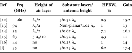
In recent times, Millimeter-wave (mm-wave) antennas, where they play the role of a key element in mm-wave communication systems, have proved to be of interest to researchers. Microstrip antennas have been worthy candidates in normal wireless systems because they have low profile, low cost, and easy to integrate. Designing antennas in the mm-wave band, which have to deal with high atmospheric debilitation, causes other serious problems such as short-range effect. To overcome this problem, the beam-steering technique and high gain antenna have been used [Reference Ko and Lee1–Reference Alreshaid, Sharawi, Podilchak and Sarabandi9]. The first step in implementing a beam-steering antenna is by designing a radiation element that is smaller in size and possesses stable characteristics. To provide point-to-multipoint and short-range applications like indoor wireless personal area networks (WPAN) without considering the position of the users, the mm-wave antennas are required to have a wide beamwidth [Reference Lee and Lee2–Reference Artemenko, Mozharovskiy, Maltsev, Maslennikov, Sevastyanov and Ssorin4]. As is well known, the rectangular patch antenna has a relatively narrow half power beamwidth (HPBW) at a half wavelength (TM010) mode which makes it difficult to attain a stable performance with an indoor WPAN. To solve this problem, a high dielectric substrate can be used; however, this leads to other problems including a narrow bandwidth (BW) and low radiation efficiency. Basically, a beam-forming network (BFN) provides the amplitudes and phases to the radiating elements to deliver the desired beams. Different techniques have been offered to achieve BFN, such as the Blass matrix, the Nolen matrix, the Rotman lens, and the Butler matrix [Reference Karamzadeh, Rafii, Kartal and Virdee6, Reference Karamzadeh, Rafii, Kartal and Virdee7]. Theoretically, it is a loss-free structure and its employment of minimum number of components make the Butler matrix more popular than the others [Reference Karamzadeh, Rafii, Kartal and Virdee6, Reference Karamzadeh, Rafii, Kartal and Virdee7]. In fact a number of works have focused on designing microstrip Butler matrix feed networks at mm-wave frequencies [Reference Haraz and Sebak8, Reference Alreshaid, Sharawi, Podilchak and Sarabandi9]. An integrated Butler with patches is introduced in Ref. [Reference Haraz and Sebak8]. The operating frequency was 60 GHz, providing a BW of 3 GHz. The system was built on an RT/Duroid 5880 substrate, with a dielectric constant of 2.2 and a thickness of 0.127 mm. The gain of the antennas was between 7 and 8.9 dBi. Most of the antennas for these systems were based on patches or quasi-Yagi antennas in a linear array setup. In [Reference Alreshaid, Sharawi, Podilchak and Sarabandi9], the first version of the system contains a 2 × 4 slot antenna array, integrated with its Butler feed network, while the second version is a 4 × 4 array. The measured (≤−10 dB) impedance BWs were at least 0.8 and 0.7 GHz for the 2 × 4 and the 4 × 4 arrays, respectively. In addition, the measured gain values for the two designs varied from 5 to 7 dB. Another most important problem of a beam-steering antenna is the reduction in gain while the beam of the antenna steers. Despite the high gain of reflector antennas, their applications are limited by their three-dimensional structures [Reference Hu10]. To solve this problem, the use of a Fabry-Perot structure is suggested. The Fabry-Perot structure was originally recommended to be applied in antenna design in 1956 [Reference Von Trentini11]. In recent dedications, various Fabry-Perot antennas in mm-wave applications have been reported [Reference Alreshaid, Sharawi, Podilchak and Sarabandi9–Reference Hosseini, Capolino and De Flaviis16]. A comparison between these works is shown in Table 1. As seen, in all of them [Reference Sauleau, Coquet and Matsui12–Reference Hosseini, Capolino and De Flaviis15] except [Reference Hosseini, Capolino and De Flaviis16], air layer is presented above radiating elements. It is difficult to perfectly fix the height of the air layer in mm-wave band designs. As a result, antenna performance is severely affected. In order to improve lower profile problems of the Fabry-Perot antenna, the dielectric layers were replaced for the air layers in some projects [Reference Hosseini, Capolino and De Flaviis16]. To address this issue, we present a stable broadside pattern which was produced by designing an antenna element with an aperture-coupled feed into a hybrid antenna with a wide beamwidth, via combining the zero-order resonance (ZOR) mode with TM010 mode[Reference Ko and Lee1–Reference Ko and Lee3]. Despite reducing the distance between antenna elements to increase the HPBW, elements are isolated from each other, which is suitable for the smaller sized mm-wave antennas. To optimize the widest beam antenna, TM010 and ZOR mode are synthesized. In addition, a modified network with a broadband 45° phase shifting and a 90° patch coupler is used to improve the Butler matrix. To improve the gain of the proposed beam-steering antenna, a novel mm-wave Fabry-Perot antenna is designed at 35 GHz. The Fabry-Perot resonator cavity is composed of the partially reflective surface (PRS) cover. The performance of the proposed antenna undergoes a trade-off among high gain, broad BW, and low profile. Table 1 illustrates a comparison between the reported Fabry-Perot antennas and this work.
Table 1. Performances of the published FP antennas ([i] is this work).

The details and results of the proposed antenna are discussed in the following section.
II. ANTENNA ELEMENTS
Figure 1 displays the geometry of the proposed single antenna. The antenna consists of two substrates, separated by a ground with an aperture. The top substrate is RT/Duroid 5880 with a relative permittivity of (ε r =)2.2, a loss tangent of (tanδ = ) 0.0009, and a thickness of (h 1 =) 0.508 mm. It contains the radiating elements. The other substrate is the Rogers 3010 (ε r = 10.2, tanδ = 0.0035), connected to a microstrip feed line. Each radiating element includes a mushroom antenna and a parasitic ring patch. The antenna produces a TM010 mode with a directional radiation pattern and a ZOR mode with an omnidirectional radiation pattern, respectively. The two modes are then synthesized to make a wide E-plane HPBW. The equivalent circuit of the antenna is demonstrated in Fig. 2 [Reference Ko and Lee1–Reference Lee and Lee2]. It comprises an aperture (C 1, C a, L a, and R a), a parasitic ring patch antenna (C p, L p, and R p), and a mushroom antenna (C R, L L, and R m). Γ m, Γ p, and Γ pm are the coupling coefficients between an aperture and a mushroom, an aperture and a parasitic ring patch, as well as between a mushroom and a patch, respectively. The equivalent elements of the antenna are extracted as follows:

Fig. 1. Configuration of proposed ZOR antenna element: (a) perspective view and (b) side view.
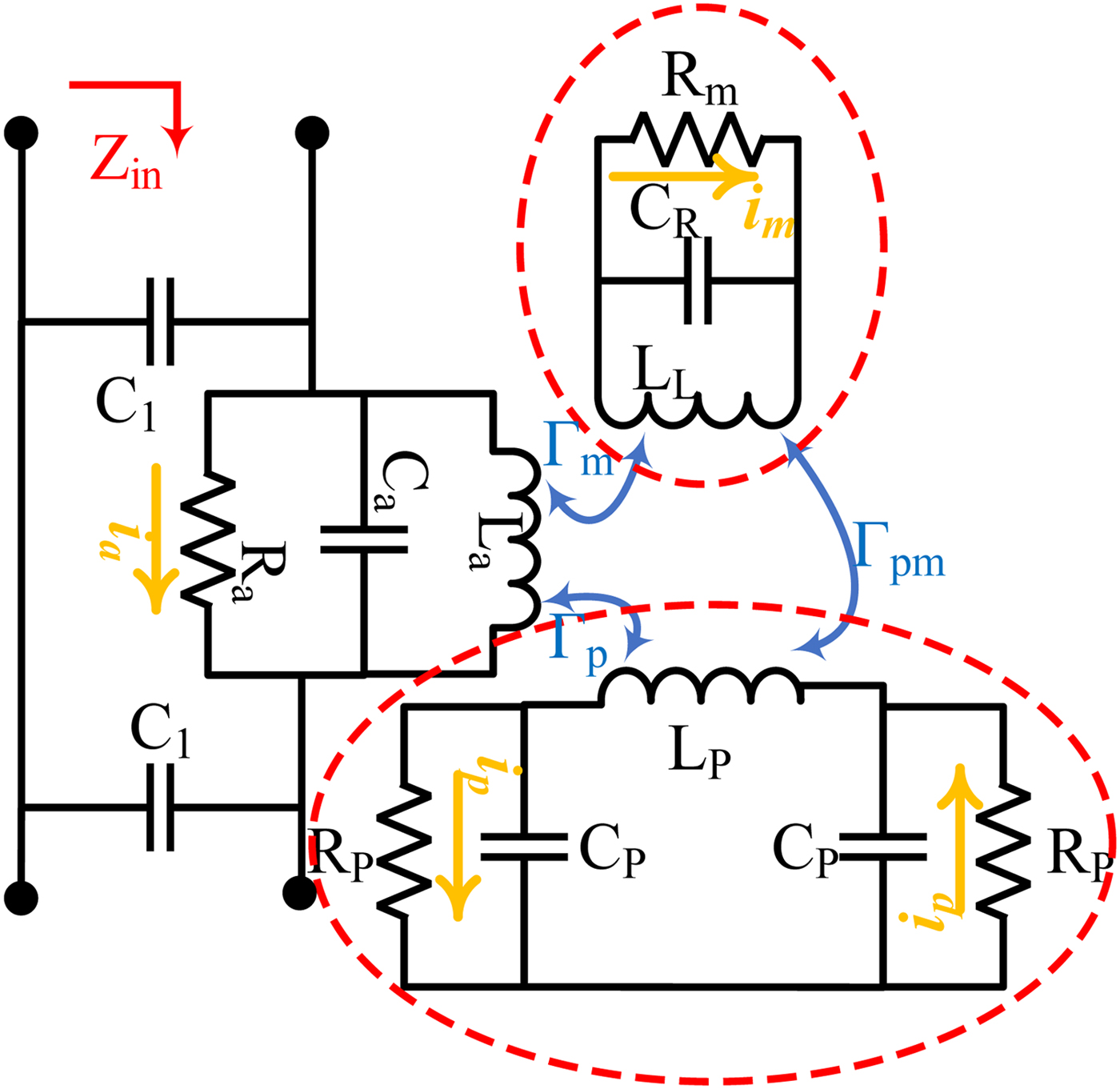
Fig. 2. Equivalent circuit of single element.
C 1 = 8.82 fF, C a = 139.54 fF, L a = 160.99 nH, R a = 2295 X, C p = 52.61 pF, L p = 765.08 nH, R p = 905 X, C R = 92.22 pF, L L = 206.01 nH, R m = 778 X, Γ m = 0.132, Γ p = 0.123, and Γ pm = 0.085.
The first step is to model the mushroom with a resistor–inductor–capacitor network. The formulas to represent a resonator as a parallel resonant circuit, when the resonator is coupled to the excitation source, can be found in [Reference Ko and Lee1–Reference Artemenko, Mozharovskiy, Maltsev, Maslennikov, Sevastyanov and Ssorin4] and [Reference James and Hall17]. The equivalent sheet inductance denoted by L L, and the equivalent sheet capacitance denoted by C R are given in [Reference James and Hall17]. The properties of the parasitic patch characteristic can be obtained by using:
 $$L_P = \displaystyle{{\mu _0/2l_{avg}} \over 4}[Ln\left( {\displaystyle{{l_{avg}} \over w}} \right) - 2],$$
μ 0 is the vacuum permeability and l avg is the average strip length calculated over all of the rings.
The second step is to find the input impedance of the slot, which is calculated by the method suggested in [Reference James and Hall17]. The impedance of a microstrip is introduced as follows:
 $$Z_{slot} = Z_c\displaystyle{{2R} \over {1 - R}},$$
where Z c is the characteristic impedance of the transmission line and R is the voltage reflection coefficient; and W a, L a, and h are the slot width, slot length, and the substrate height, respectively. The mutual inductance between the microstrip patch and parasitic patch can be introduced as:
 $$M = \displaystyle{{\mu _0x_1} \over {2\pi}} \left[ {0.467 + \displaystyle{{0.059w^2} \over {x_1^2}}} \right],$$
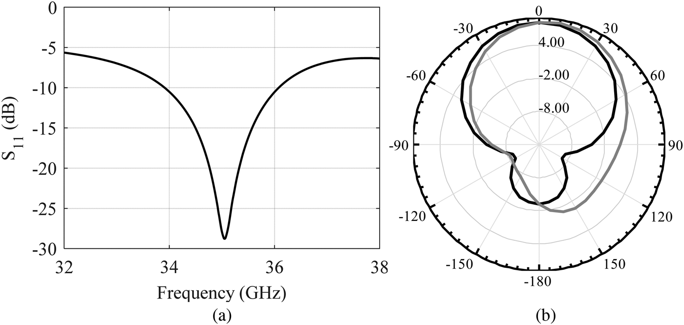
where w is the patch width (W p) and x 1 is the effective parasitic patch length. Finally, by optimizing results by Agilent advanced design system (ADS), the values of the equivalent circuit are attained. Figure 3 illustrates the comparison between the proposed antenna with the simulated mutual coupling and a simple patch in the 0.35 λ0 distance. Clearly, this structure (with more than about 15 dB lower coupling of elements) is superior to the simple patch. Figure 4 shows the simulated S 11 and pattern at 35 GHz. As can be seen from the figure, the simulated frequency resonance occurs at 34.9 GHz. The simulated E-plane HPBW and peak gain are 138° and 7.21 dBi, respectively. Compared with a simple patch at 0.35 λ0 antenna, an advantage of the proposed antenna is the low mutual coupling between its elements. The optimal dimensions of the antenna are as follows: W p = 2 mm, W h = 1.3 mm, radius of the via (V r) = 0.1 mm, L a = 2 mm, W a = 0.1 mm, h 1 = 0.508 mm, h 2 = 0.25 mm, and L stub = 1 mm. The parameters are obtained from full wave simulation (ANSYS HFSS). The size of the patch antenna (W p) and hole (W h) are determined to achieve the resonance frequency at 35 GHz. Size of the aperture (L a) and radius of via (V r) are set to optimize the radiation efficiency of the mushroom antenna [Reference Lee and Lee2].
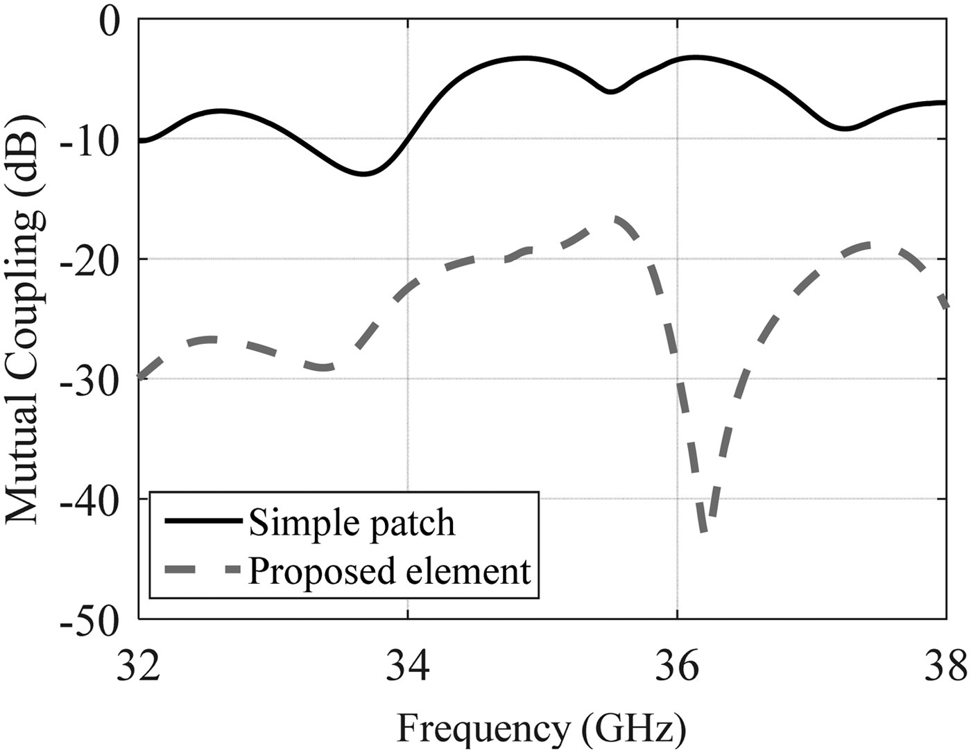
Fig. 3. Comparison between simulated mutual coupling of proposed antenna with simple patch at 0.35 λ0 distance.

Fig. 4. The simulated results of proposed antenna elements at (a) S 11 and (b) pattern at 35 GHz.
III. PRS CELL DESIGN
The PRS is embedded on the top layer of the antenna. The electromagnetic wave in this cavity is excited by the dual ZOR antenna element. A simple optical ray model can be used to analyze the antenna [Reference Haraz and Sebak8]. The resonant condition of the Fabry-Perot antenna can be written as:
 $$\varphi _g + \varphi _r - \displaystyle{{4\pi h} \over \lambda} = 2N\pi, $$
 $$N = 0, \,\pm 1, \,\pm 2, \ldots $$
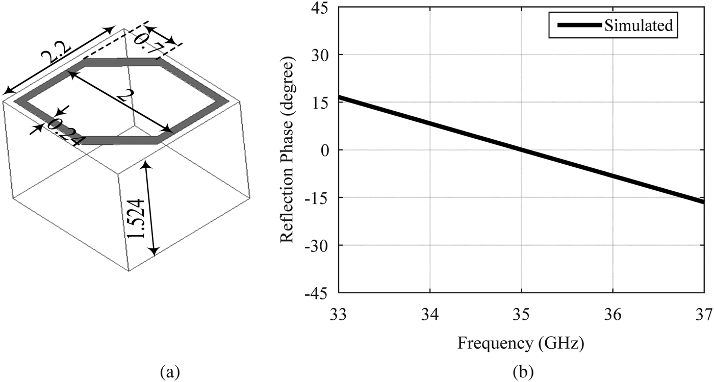
where h is the height between the PRS and the ground, φ g is the reflection phase of the metal ground plane, φ r is the reflection phase of the PRS, and λ is the operation wavelength in the substrate. The structure of the proposed PRS unit cell is displayed in Fig. 5(a). As shown in Fig. 5(b), and comparison with (4), the proposed unit-cell structure has a resonance condition at 35 GHz. In this structure, the ground of the middle layer plays its role as a ground PRS, which must be considered in simulation.

Fig. 5. The proposed PRS structure and result: (a) dimensional of proposed unit cell and (b) reflection phase diagram of PRS unit cell.
IV. MODIFIED BUTLER MATRIX AND 45° PHASE SHIFTER
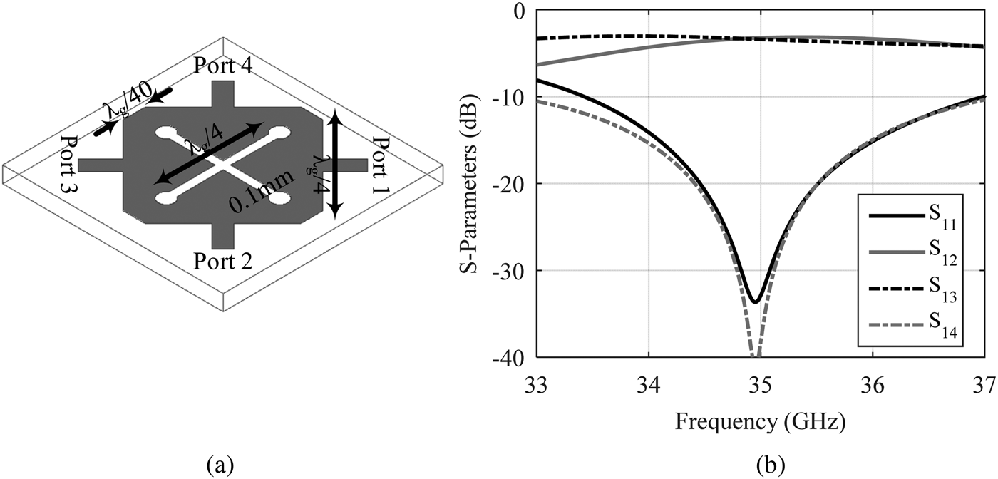
The proposed Butler matrix is simulated and optimized by the Agilent ADS. The configuration of the modified Butler matrix feed network consists of four 90° patch couplers and two novel broadband 45° phase shifters, printed on a Rogers 3010 substrate with a 0.25 mm thickness. This result is presented in Fig. 6. The proposed Butler matrix includes four input ports and four output ports, and the distance between the output feeding lines (at 0.35 λ0) is 35 GHz (λ0–35 GHz – wavelength in free space at 35 GHz). One of the most important steps in designing a modified Butler matrix is the creation of a broadband 45° phase shifter. Its structure and results are shown in Fig. 7. As illustrated in Fig. 7, the proposed phase shifter comprises two L-shapes and a rectangular stub. This design creates a phase constant and it can change the size of phase shift. Use of this method leads to a broadband phase shifter from 33 to 36.8 GHz. Error of the phase shifter is ±5°. The structure of a 90° patch coupler is illustrated in Fig. 8. The advantage of this design, compared to the regular 90° branch line coupler, is its small structure. This powers the structure in reducing fabrication error and its integration. As shown in Fig. 8(b), the magnitude of the scattering parameters shows a resonance and −3 dB power, dividing at 35 GHz. By selecting each input (of four ports) as a driving input, the Butler matrix delivers four output signals with equal amplitude (−6 dB) and phase differences of 45, 90, 135, and 180°. As a result, matrix can arrange beam steering at different broadside angles in a transverse plane perpendicular to the substrate.
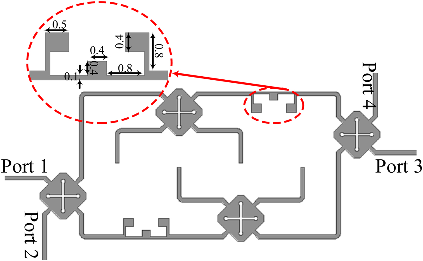
Fig. 6. The configuration of modified Butler matrix feed network with broadband phase shifting.
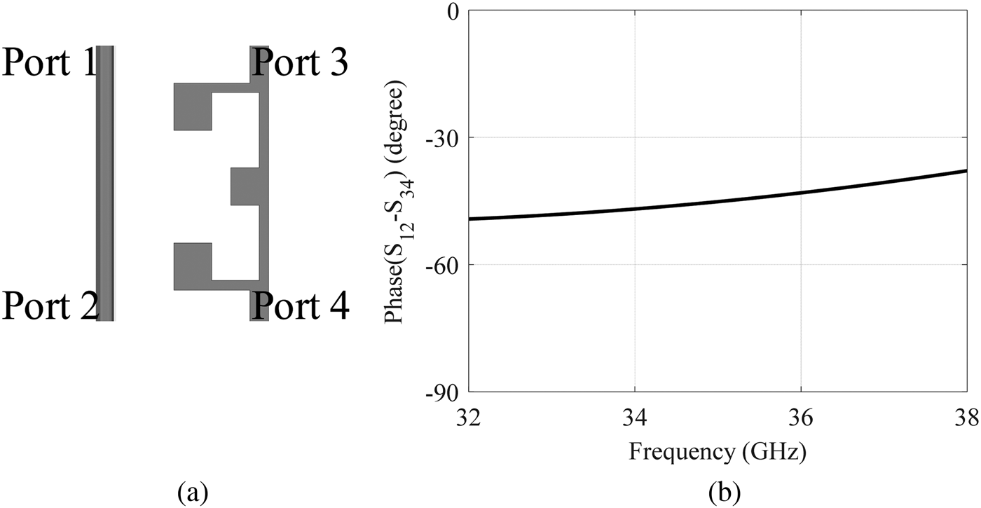
Fig. 7. The structure and results of broadband 45°phase shifter: (a) structure and (b) phase shifting.

Fig. 8. The configuration proposed 90° patch coupler and result: (a) configuration and dimension, and (b) magnitude of scattering parameter.
V. RESULTS AND DISCUSSION
The proposed beam-steering array antenna was fabricated and measured. The multi-layered configuration and fabricated antenna are illustrated in Fig. 9. The scattering parameters of the proposed antenna were performed with an Agilent 8510XF (E7340A) network analyzer. As displayed in Fig. 10, the measured results for S ii (Fig. 10(a)) are in a reasonable agreement with the simulated ones [Reference Karamzadeh, Rafii, Kartal and Virdee6–Reference Karamzadeh, Rafii, Kartal and Virdee7]. From the Butler matrix feed network structure, it can be concluded that the antenna acts as a nearly symmetrical structure. Hence, only the simulated results of ports 1 and 2 are presented. From the measured results, a good impedance BW over the frequency range of 33.84–36.59 GHz can be attained (as shown in Fig. 10(a)). The isolation of the input ports is shown in Fig. 10(b). From this figure, it can easily be understood that a good isolation (<−12 dB) is available. The simulated upper hemisphere gain patterns at 35 GHz are presented in Fig. 11.

Fig. 9. The configuration and a sample of fabricated proposed beam-steering antenna: (a) multi-layered view and (b) fabricated antenna.
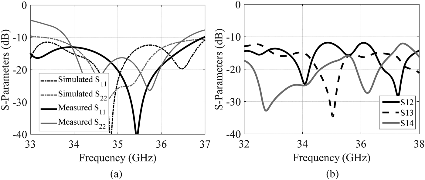
Fig. 10. Scattering parameters of proposed antenna array: (a) comparison between simulated and measured S ii, (b) measured S ij.

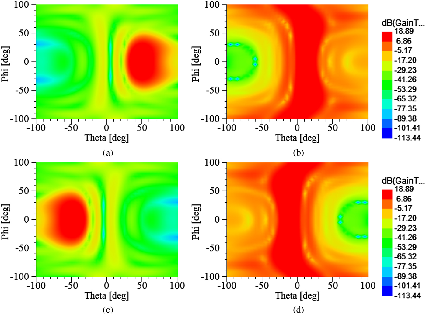
Fig. 11. Simulated gain patterns corresponding to ports 1–4 at 35 GHz: (a) port 1, (b) port 2, (c) port 3, and (d) port 4.
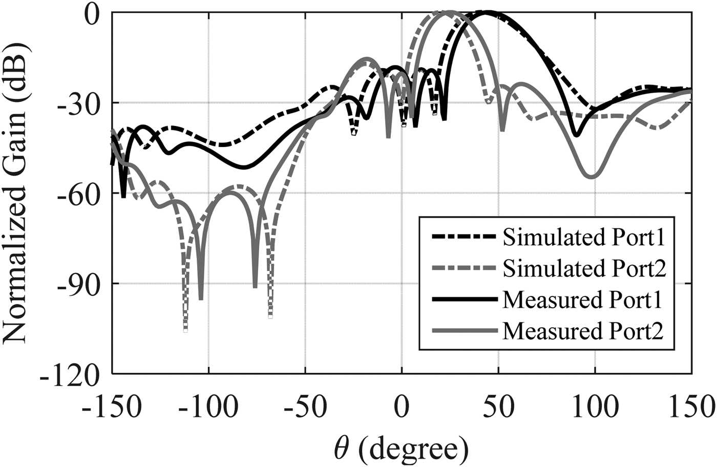
The simulations proved that the presented array has good results in four-port beam-forming applications. The comparison between simulated and measured patterns at 35 GHz is presented in Fig. 12. In order to measure radiation patterns, an MI Technology anechoic chamber is used. In this method, a horn antenna is used to provide a plane wave toward the antenna under test. This antenna is located at the focal point of the reflector [Reference Ko and Lee1–Reference Karamzadeh, Rafii, Kartal and Virdee7]. To ensure clear judgment, the patterns are correspondingly normalized by the measured peak gains. The normalized measured radiation pattern of the planar microstrip antenna at 35 GHz with a 4 × 4 Butler matrix is shown in Fig. 12. As clearly presented in the figure, the pattern direction varies by changes in input ports. The beams were successfully steered from broadside, with peak gains ranging from 15.4 to 17.6 dBi. The measured gains at 35 GHz for ports 1, 2, 3, and 4 are 16.2, 17.4, 17.3, and 15.9 dBi, respectively. The whole triangular array grid dimension is optimized to maximize the single-element performance in an array radiating environment.

Fig. 12. The comparison between normalized simulated and measured radiation patterns of the planar microstrip antenna array at 35 GHz for ports 1 and 2.
VI. CONCLUSION
In this work, a novel compact broadband beam-steering antenna has been introduced. A new Butler matrix is used for feed network. In order to have a high gain and broadside pattern, the ZOR antenna elements were set at 0.35 free space wavelength. A novel feed network was designed using a 90° patch coupler and broadband 45° phase shifters, which are optimized to achieve a compact size and wide BW performance. The obtained results introduce a beam-steerable antenna which uses a Fabry-Perot layer without the height of the air layer, which correct the gain features of the delivered beam, with an acceptable gain in the desired impedance BWs. This antenna can be used in many applications such as the 5 G mobile and automotive radar applications.
ACKNOWLEDGEMENT
The authors would like to thank Premier Frequency for the test and fabricated antenna and they also appreciate Professor Bal. S. Virdee for the help provided to realize this project.
 Asghar Bakhtiari was born in Miyaneh, Iran, in 1975. He received M.Sc. degrees in Electrical Engineering from Islamic Azad University South Tehran Branch, Tehran, Iran, in 2002. He is a Ph.D. student at Science and Research Branch, Islamic Azad University, Tehran-Iran. Currently, he is with the Faculty of Engineering, Takestan Branch, Islamic Azad University, Takestan-Iran. His research interests include metamaterials, miniaturized antennas, electromagnetic, EMC/EMI, and photonics.
 Ramezan Ali Sadeghzadeh is a full professor of Communications Engineering at the Faculty of Electrical Engineering of the K.N. Toosi University of Technology. He received his B.Sc. in 1984 in Telecommunication Engineering from the K.N. Toosi, University of Technology, Tehran Iran, and M.Sc. in Digital Communications Engineering from the University of Bradford and UMIST (University of Manchester Institute of Science and Technology), UK as a joint program in 1987. He received his Ph.D. in Electromagnetic and Antenna from the University of Bradford, UK in 1990. He worked as a Post-Doctoral Research Assistant in the field of propagation, electromagnetic, antenna, bio-medical, and wireless communications from 1990 till 1997. From 1984 to 1985, he was with Telecommunication Company of Iran (TCI) working on Networking. Since 1997 he is with the K.N. Toosi University of Technology working with Telecommunications Department at the Faculty of Electrical Engineering. He has published more than 180 referable papers in international journals and conferences. Professor Sadeghzadeh current interests are numerical techniques in electromagnetic, antenna, propagation, radio networks, wireless communications, nano-antennas, and radar systems.
 Mohammad Naser-Moghadasi was born in Iran, in 1959. He received the B.Sc. degree in Communication Engineering in 1985 from the Leeds Metropolitan University (formerly Leeds Polytechnic), UK. Between 1985 and 1987, he worked as an RF-design engineer for the Gigatech company in Newcastle Upon Tyne, UK. From 1987 to 1989, he was awarded a full scholarship by the Leeds Educational Authority to pursue an M.Phil. on Studying CAD of microwave circuits. He received his Ph.D. in 1993, from the University of Bradford, UK. He was then offered a 2-year post-doc at the University of Nottingham, UK, to pursue research on microwave cooking of materials. From 1995, Dr. Naser-Moghadasi joined Islamic Azad University, Science and Research Branch, Iran-Tehran, where he currently is the head of postgraduate studies. His main areas of interest in research are microstrip antenna, microwave passive and active circuits, RF MEMS. Dr. Naser-Moghadasi is member of the IET, MIET, and IEICE. He has so far published over 200 papers.