


I. INTRODUCTION
Micro-electromechanical systems (MEMS) are integrated microdevices combining electrical components with passive (sensing) and active (actuation) interface functions to their physical surroundings. Typical examples for sensors include pressure sensors, microphones, accelerometers, gyros, and gas sensors, and examples for actuator functions include inkjet print-head nozzles, gas valves, microswitches, and optical micromirror arrays for projection devices [Reference Kovacs1–Reference Madou3].
Radiofrequency (RF) MEMS are MEMS devices that are interacting with electrical signals from DC up to sub-millimeter waves, by switching, modulating, matching, tuning, and filtering. Typical devices are micromachined switches [Reference Rebeiz4, Reference Brown5], mechanically tunable capacitors [Reference Nguyen6], micromachined inductors [Reference Jiang, Wang, Yeh and Tien7], micromechanical resonators for filters and as frequency base [Reference Nguyen8], tunable loaded lines for phase shifters [Reference Rebeiz, Tan and Hayden9] or impedance-matching circuits [Reference Papapolymerou, Lange, Goldsmith, Malczewski and Kleber10], reconfigurable antennas [Reference Cetiner, Qian, Chang, Bachman, Li and De Flaviis11], and three-dimensional (3D) micromachined transmission lines [Reference Llamas-Garro and Corona-Chavez12]. In general, RF MEMS devices are characterized by near–ideal signal handling performance in terms of insertion loss, isolation, linearity, large tuning range, and by keeping these performance parameters over a very large bandwidth [Reference Rebeiz4, Reference Tilmans, De Raedt and Beyne13].
Microwave MEMS are RF MEMS devices that operate with signal frequencies above 30 GHz. With applications moving to higher frequencies, the performance advantages of MEMS devices over their competitors are getting larger. Also, at frequencies where the signal wavelengths are getting closer to the device dimensions, it is possible to miniaturize a complete RF system on a chip, and different ways of interaction between the microwave signals and the micromechanics lead to new possibilities of RF MEMS devices [Reference Sterner, Chicherin, Räisänen, Stemme and Oberhammer47].
Operational reliability, i.e. the ability of devices to work as specified over the whole lifetime, and robustness to process parameter variations, are key issues in RF MEMS design [Reference Hartzell, da Silva and Shea14, Reference DeNatale and Mihailovich48].
Conventional RF MEMS designs are still characterized by some fundamental problems. Thin metallic bridges, for instance, found in many RF MEMS devices, such as switches and phase shifters, are susceptible to temperature-accelerated creep and fatigue, limiting the device life-time [Reference Hartzell, da Silva and Shea14]. In contrast, monocrystalline silicon is a very robust MEMS structural material that is at the same time also suitable as RF dielectric material if high-resistivity silicon (HRS) is used [Reference Petersen15, Reference Lederer and Raskin49].
Dielectric charging is another major reliability issue in electrostatically actuated RF MEMS [Reference Wibbeler, Pfeifer and Hietschold17, Reference Goldsmith, Ehmke, Malczewski, Pillans, Eschelmann, Yao, Brank and Eberly18]. Trapped charges in dielectric isolation layers and in the substrate change the characteristics of the device, leading to actuation voltage drift and reduced RF performance. Some suggested solutions in the literature, for instance, are tailor-made actuation voltage shapes (pulsed or bi-polar) to reduce charge build-up [Reference Reid and Webster19, Reference Herfst, Steeneken and Schmitz20], reduced actuation voltage to minimize the field strength in the dielectric [Reference Reid and Webster19, Reference Herfst, Steeneken and Schmitz20] and dielectrics with fast charging recovery time like diamond [Reference Sullivan, Friedmann and Hjort21–Reference Chee, Kami, Fisher and Peroulis23]. Dielectric-less designs, using metal stoppers for isolation, e.g., is a promising alternative to the conventional solutions [Reference Mardivirin, Pothier, Crunteanu, Vialle and Blondy24–Reference Sterner, Roxhed, Stemme and Oberhammer26].
The lifetime of RF MEMS metal-contact switches is typically limited to contact degradation and the switches die in short circuit (contact stiction). Most switches rely on a passive mechanical spring opening mechanism that is typically not enough to overcome the stiction forces, although it can be increased at the expense of higher actuation voltage [Reference Mercado, Koo, Lee and Liu28]. Soft metals like gold, which are preferred from an electrical perspective, are the most susceptible to contact stiction [Reference Coutu, Kladitis, Leedy and Crane27]. Large attention has, therefore, been given to hard contact material stacks – Cu/W/Au, rhodium (Rh), tungsten (W), molybdenum (Mo), palladium (Pd, Ag/Pd, Au/Ag/Pd, Au/Pd), silver/tungsten/rhodium (Ag/W/Rh), Ag/W/CdO, and ruthenium (Cr/Ru/Au/Ru), e.g. – which promise reliable contact performance at the expense of higher contact force requirements [Reference Johler29–Reference Ke, Miao and Oberhammer35]. However, soft material contact reliability can be greatly improved if an active opening or push–pull mechanism is used [Reference Chiao, Fu, Lin and Choudhury36–Reference Hah, Yoon and Hong39].
Many RF MEMS designs are based on multilayer free-standing structures, requiring a stack of different structural, isolating, and conducting materials. Controlling the residual stress and achieving temperature compensation in these structures are very difficult due to the diverse material properties. Significant process optimization is necessary and the resulting residual stress and temperature compensation are very sensitive to process parameter variations [Reference Duffy, Bozler, Rabe, Knecht, Travis, Wyatt, Keast and Gouker43, Reference Chen, Miao, Guo and Lin44, Reference Siegel, Ziegler, Prechtel, Schonlinner and Schumacher46].
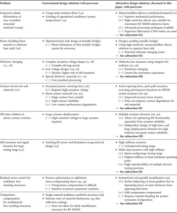
In this paper, we review work done in our group on RF MEMS designs with features addressing these fundamental problems of conventional RF MEMS designs. An overview of these design problems, conventional designs, and proposed novel design concepts addressing these problems is shown in Table 1.
Table 1. Overview of major fundamental design problems of conventional RF MEMS devices and novel design concepts addressing these issues as discussed in this paper.
II. DESIGN FOR PROCESS ROBUSTNESS AND OPERATIONAL RELIABILITY
In a conventional MEMS design cycle, reliability is controlled by failure mode analysis of prototypes and step-by-step improvement of the design. This reduces the effect of the failure modes, but often does not solve the underlying fundamental problems. Conventional solutions might also impose heavy constraints on the process design or reduce robustness to variations in material and process parameters. An example is dielectric charging in electrostatic actuators, which can be mitigated but has not been solved sufficiently despite very extensive failure analysis [Reference Rebeiz4, Reference Wibbeler, Pfeifer and Hietschold17–Reference Chee, Kami, Fisher and Peroulis23].
Instead, we propose trying to avoid such problems by using different design concepts rather than by failure mode suppression. By designing MEMS for operational reliability it is possible to completely eliminate or be less susceptible to certain failure modes, and to changes in operating conditions. Furthermore, the fabrication process should be designed to be robust to material and process variation, removing the need for costly process tuning for high device uniformity.
The following design features for operational reliability and process robustness, also outlined in Table 1, are demonstrated by RF MEMS devices discussed in this paper:
– Monocrystalline silicon structures for high mechanical lifetime, high-temperature stability, and high reproducibility of accurate mechanical movements.
– All-metal electrostatic MEMS actuators to avoid dielectric charging as no dielectric isolation layers are utilized.
– Reversing active/passive function in MEMS switch actuators to improve contact performance, especially for soft contact materials.
– Independent design of high-force and large-displacement in MEMS switch actuators which allows for optimizing RF functionality separately from actuator reliability.
– High-stiffness multi-step actuators enabling large tuning range, but still maintaining low susceptibility for self-actuation and high signal linearity.
– Designs eliminating metallic bridges for high–power handling, improved mechanical life-time, and stable pull-in and pull-out voltages over high cycle numbers.
– Full stress-gradient control and temperature compensation of metalized silicon membranes, very robust to process and material property variation, by symmetric anti-parallel deposition.
– The fabrication of all presented devices is only utilizing standard micromachining processes in standard semiconductor manufacturing equipment, which allows for yield optimization and thus high-volume industrial production.
In the following subsections, these design concepts are further discussed.
A) Monocrystalline silicon as structural and electrical material for RF MEMS
Even if, in recent years, silicon micromachining has been rapidly augmented with new material and processes [Reference Liu2], monocrystalline silicon, besides silicon carbide, still is the most robust and reliable structural material for micromachined devices [Reference Oberhammer, Sterner and Somjit50]. Its yield strength exceeds steel by a factor of 2 – 3, and maintains elastic properties under high stress levels even when exposed to elevated temperatures, and is very well characterized [Reference Petersen15].
Monocrystalline silicon is available as a high-purity low-cost substrate in many different sizes and crystal orientations, can be supplied in a large variety of doping levels, can be polished to very high surface quality, and has good thermal conductivity. As a result of these advantages, in combination with silicon offering the largest variety of stable and standardized wafer-scale micromachining processes and highly developed etching tools, silicon is still the best suitable material for integrated microsystems with high demands on mechanical reliability [Reference Kovacs1]. Monocrystalline silicon has been successfully applied to a variety of MEMS devices including pressure sensors, accelerometers [Reference Fujita, Fukumoto, Suzuki and Maenaka51], undeformable sub-nm-flatness micromirror arrays [Reference Niklaus, Haasl and Stemme52], and robust microrelays [Reference Sakata, Komura, Seki, Kobayashi, Sano and Horiike53, Reference Weber, Lang and Slocum54].
Besides silicon being an excellent structural material for MEMS moving elements, HRS is also a promising substrate material for Radio Frequency Integrated Circuit (RFIC) technology. HRS substrates, including silicon-on-insulator (SOI) wafers, are available at continuously falling costs with a controllable bulk resistivity up to 8 kΩcm, and sufficiently low dielectric losses with a tan δ of 6 × 10⁻⁴. However, for transmission lines fabricated on HRS substrates, free carriers within the interface between the silicon and the silicon dioxide layer on the surface reduce the effective resistivity by more than one order of magnitude, which necessitates the application of surface passivation techniques [Reference Lederer and Raskin49, Reference Oberhammer, Sterner and Somjit50].
Conventional RF MEMS devices for microwave applications are most often based on movable thin metallic bridges, for instance, employed as capacitive switches [Reference Goldsmith, Ehmke, Malczewski, Pillans, Eschelmann, Yao, Brank and Eberly18] or as tunable capacitors for distributed MEMS transmission line (DMTL) phase shifters [Reference Rebeiz, Tan and Hayden9]. In contrast to silicon, such metallic bridges have the disadvantage of being susceptible to plastic deformation at high cycle numbers, especially at slightly elevated temperatures above 80°C where gold, the most favored material because of its low resistivity, quickly loses its elastic properties. Furthermore, these bridges must be thin enough for actuation at acceptable actuation voltages which drastically limits the power handling [Reference Oberhammer, Sterner and Somjit50].
Monocrystalline silicon is used as structural material for all the devices dealt with in this paper.
B) All-metal electrostatic MEMS devices for avoiding dielectric charging
Dielectric charging occurs whenever the electrical field in electrostatic actuators is concentrated in a dielectric material, such as the isolation layers employed in conventional MEMS electrostatic actuator designs to prevent contact and thus short-circuiting between the actuator electrodes. Therefore, the easiest way to prevent charging is to use a design that does not require dielectric materials for isolation. Instead of isolation layers, metal stoppers are typically used [Reference Mardivirin, Pothier, Crunteanu, Vialle and Blondy24–Reference Sterner, Roxhed, Stemme and Oberhammer26]. In contrast to common belief, the tuning range of dielectric-less actuator does not decrease, but the actuation force, especially for pull-in, is reduced as compared to actuators utilizing dielectrics.
All-metal dielectric-less actuators are used in the devices in subsections IIIB and IIIC.
C) Reversing active/passive functions in MEMS switch actuators
In a conventional MEMS electrostatic actuator, the active force is provided by the electrostatic force and the mechanical elasticity of the structural material is used for creating the passive restoring force. For ohmic MEMS switches, this typically means that the contact force of the switch is large, due to the non-linear behavior of the electrostatic force, but that the opening force is much weaker. However, for softer contact materials, the force required for establishing a good electrical contact in the closed state is actually much less than the force needed to overcome the contact stiction when opening the switch. Therefore, it is better for softer contact materials, to design the switch in a way that the electrostatic force is used to actively opening the switch, and that the mechanical spring force is used to close the switch, i.e. in reversed order as compared with conventional designs [Reference Oberhammer and Stemme37].
Such reversed active/passive switch actuator function is demonstrated by the multi-stable switches in subsection IIIC.
D) Multiple actuator elements for independent design of force and displacement
The off-state isolation of an RF MEMS series switch is, to a large extent, determined by the gap between the switch contacts. A compromise is required between having a large gap, and thus a large isolation, a low actuation voltage, and reliable contact separation, since an electrostatic actuator with a large displacement range will either be weak or have a very large actuation voltage. However, by employing multiple actuator elements, one of them can provide a large displacement range, and thus a large off-state isolation, and the other can provide the strong force required for reliable operation [Reference Sterner, Roxhed, Stemme and Oberhammer26, Reference Jang, Lee, Kim and Kim40].
Such independent optimization of the RF isolation and the actuator reliability is performed for the two separate interlocking switch cantilevers of the switch designs in subsection IIIC.
E) Multi-step quasi-analog high-stiffness actuators for high signal linearity and self-actuation robustness, at a large tuning range
In tunable RF MEMS transmission line elements, such as capacitors or phase shifters, the moving elements are typically affected not only by the electrostatic forces between the actuator's electrodes but also by an electrostatic force created by the RF signal between the signal line and the moving electrode, due to the non-linearity F el ∝ V Reference Liu2, which results in a constant electrostatic force proportional to the effective voltage value of a stationary RF signal, even for RF signal frequencies far beyond the mechanical resonance frequency. This phenomenon may, in a worst case, result in self-actuation, but even for small signals cause self-modulation by the power level of the RF signal, destroying the signal linearity of the device. A conventional work-around comprises using a high-stiffness actuator that reduces the problem at the expense of increased actuation voltage. For the dielectric-block phase shifter presented in subsection IIIA such a compromise is made between reasonable actuation voltage and good RF signal linearity.
For the tunable capacitors in subsection IIIC, a novel multi-step actuator is used, which has the advantage of providing a very large tuning range, while still maintaining excellent high linearity over the entire tuning range, as the stiffness of the different actuators is increasing for smaller electrode distances, where conventional tunable capacitors experience the highest non-linearity.
F) Symmetric composition of structural layers for stress gradient and temperature compensation
RF MEMS designs typically require multilayered moving elements, for instance, electrode metallization on an insulating structural material. Multilayers result in bending due to stress gradients that are difficult to control, especially for a large temperature range.
Stress gradients in conventional MEMS multilayer structures are often compensated by specifically tuned counter-stressed layers, which require careful tuning of the fabrication process and are sensitive to process variations. However, such a compensation strategy is only feasible for a small operation temperature range, due to the non-matching coefficients of thermal expansion (CTE) of the different layers.
By using symmetrical anti-parallel metal deposition, as discussed in this paper, a monocrystalline-silicon-core freestanding membrane can be coated by a thick metal layer without residual stress and with full temperature compensation [Reference Sterner, Stemme and Oberhammer45]. This novel technique is used for the MEMS tunable microwave surfaces in subsection IIIB.
III. EXAMPLES OF MICROWAVE MEMS DEVICES BASED ON DIFFERENT DESIGN CONCEPTS
A) Monocrystalline-silicon dielectric-block phase-shifters
This section shows a novel multistage all-silicon microwave MEMS phase-shifter concept [Reference Somjit, Stemme and Oberhammer55–Reference Somjit, Stemme and Oberhammer57]. The concept is based on multiple-step deep-reactive-ion-etched monocrystalline-silicon dielectric blocks that are transfer bonded to an RF substrate containing a 3D micromachined coplanar-waveguide (CPW) transmission line, and features the following design elements for improved reliability over conventional MEMS phase shifters, i.e. DMTL phase shifters and MEMS switched true time-delay (TTD) networks, all based on moving thin metallic bridges, as shown in Fig. 1:
– All mechanical parts, including the moving block, mechanical springs, and support anchors, are etched out of the same, continuous monocrystalline silicon bulk layer for best mechanical reliability, in contrast to thin metallic bridges prone to plastic deformation.
– The dielectric constant of the moving block can be tailor-made in a wide range by varying the etch hole size.
– As dielectric blocks are used for the tuning, the power handling is only limited by the transmission line, in contrast to conventional phase shifters where currents induced in the thin bridges result in substantial device heating and thus power limitation.
– No detectable dielectric charging as no closed dielectric isolation layer is used.
– Reduced substrate losses and substrate charging by deep-etched grooves in the transmission line.

Fig. 1. Comparison between two conventional phase shifter concepts and the presented novel dielectric-block phase shifter: (a) switched TTD network [Reference Rizk and Rebeiz58]; (b) DMTL phase shifter [Reference Hayden and Rebeiz59], and (c) novel dielectric-block phase shifter [55–57].
1) Concept
A single stage of the novel phase shifter concept is depicted in Fig. 1(c), together with two conventional TTD and DMTL phase shifter concepts in Fig. 1(a) and 1(b). A monocrystalline HRS (>4 kΩcm) dielectric block is situated on top of a 1 µm–thick gold CPW. The relative phase shift Δϕ is achieved by vertically moving the dielectric block above the transmission line by electrostatic actuation, which results, due to the modulation of the capacitive load of the line, in varying propagation constants of the microwave signal in the transmission line. Silicon is a very suitable material for this task because of its high dielectric constant of 11.9, resulting in high sensitivity to the block position. The 50 µm–deep etched slots into the HRS substrate decrease substrate loss and decrease the effective ɛr of the transmission line, thus further increasing the sensitivity to the silicon dielectric block. The length of the dielectric block is chosen to be λ/2 at the nominal frequency of 75 GHz to minimize the RF signal reflection from both edges of the dielectric block. For digital-type operation (up-state or pulled-in), an initial distance of the block of 5 µm to the transmission line is chosen, which is an optimum operation point compromising high phase-shift sensitivity with a displacement realizable by MEMS electrostatic actuators. The silicon blocks are fabricated by polymer transfer bonding [Reference Niklaus, Enoksson, Griss, Kälvesten and Stemme60] of a complete 30 µm-thick silicon device layer from an SOI wafer to the target wafer, by subsequent removing of the SOI handle wafer and by structuring the block with its mechanical springs by different deep-reactive-ion etching steps. Dielectric charging of the block in the down-state is avoided by small SiN distance keepers [Reference Oberhammer, Sterner and Somjit50, Reference Somjit, Stemme and Oberhammer55].
For releasing the silicon block, the polymer sacrificial layer is etched through etch-holes in the block. When properly choosing the etch-hole sizes, which are of the order of 100 times smaller than the wavelength, the effective dielectric constant of the block can be tailor-made, giving the possibility of designing phase-shifter stages of different relative phase shifts out of the same material. Figure 2(a) shows an SEM picture of three stages with different etch-hole sizes, resulting in a 45°, a 30°, and a 15° phase shift. Figure 2b presents a 4.25-bit binary–coded multi-stage phase shifter constructed with these stages with 15° resolution and a maximum phase shift of 270° at 75 GHz, consisting of 5 × 45° + 1 × 30° + 1 × 15° stages.

Fig. 2. (a) Scanning electron microscopy (SEM) picture of a 45°, a 30°, and a 15° stage in series; (b) 7-stage phase shifters at 75 GHz: binary–coded 5 × 45° + 30° + 15° phase shifter [55, 56].
2) RF characterization
Figures 3(a) and 3(b) summarize the performance of the binary–coded phase shifter: the maximum insertion loss and return loss at the design frequency of 75 GHz is −3.5 and −17 dB, respectively, and the maximum insertion and return loss in the whole 75 – 110 GHz band are better than −4 and −12 dB. The phase shift per loss is 71.05 and 98.3°/dB at 75 and 110 GHz, respectively, and the phase shift per length is 490 and 716°/cm at these frequencies. These results of the first prototypes show the best maximum loss per bit and return loss ever reported for the whole W-band (except for [Reference Hung, Dussopt and Rebeiz61] which has better performance at its nominal frequency only, but performs worse for the rest of the W-band, and is fabricated on glass substrate), clearly proving the potential of this novel phase shifter concept [Reference Oberhammer, Sterner and Somjit50, Reference Somjit, Stemme and Oberhammer56].

Fig. 3. Performance of the binary–coded phase shifter for the W-band: (a) insertion loss and return loss for actuating 1 – 7 stages; (b) phase shift in all states. Non-linearity investigation; (c) relative phase shift of a 45° stage depending on signal power; and (d) intermodulation product and intercept point of third order [55, 56].
As any (MEMS) phase shifter, the moving parts in the up-state are susceptible to self-modulating their deflection, since the voltage on the signal line also exerts an attracting force, if the signal line voltage is modulated with a frequency lower than the mechanical resonance frequency (60 kHz for the presented designs). This demodulation effect of the RF signal is caused since the electrostatic force is proportional to the square of the voltage. Figure 3c shows the measured change in phase shift for a 45° stage in the up-state, depending on the signal line power. The phase error at 35 dBm signal power is still below 2%, but reaches quickly 4% at 40 dBm. This behavior results in an intermodulation intercept point of third order of 48 dBm up to a signal power of 30 dBm, which emphasizes the excellent linearity behavior of the device (Fig. 3(d)) [Reference Oberhammer, Sterner and Somjit50, Reference Somjit, Stemme and Oberhammer56].
3) Reliability and power handling
All moving parts, including the blocks and the mechanical springs, are fabricated out of the same monocrystalline silicon block. Small silicon oxide distance keepers are used instead of a full isolation layer, reducing the potentially charging area to 1.59%. No other materials are employed, guaranteeing the best reliability, which was proven by lifecycle tests. All tested devices could be actuated to 1 billion cycles in a non-hermetic environment without any failure or observed change in pull-in voltage, and after which the tests were discontinued. Also, in contrast to conventional MEMS phase shifters, where the power handling is limited by the critical current density in the thin metallic bridges, the power handling of this phase shifter concept is not limited by the moving parts, but just by the actual transmission lines and the substrate as a heat sink [Reference Oberhammer, Sterner and Somjit50, Reference Somjit, Stemme and Oberhammer55].
Figure 4 plots the simulated temperature increase of the hottest spots for the two conventional TTD and DMRL phase shifters and the presented novel dielectric-block concept, all of them at 75 GHz, over signal powers from 20 to 40 dBm (10 W). For the novel dielectric-block phase shifter (45° stage), the maximum temperature rise is only 30°C, whereas the maximum temperature rises for the TTD switch and DMTL phase shifter (45°) are as high as 650 and 300°C, respectively, which is by a factor of more than 20 and 10 times more than the novel dielectric-block phase shifter, respectively. Even if a silicon substrate, offering a better heat sink, would be used for the conventional phase shifters, which, however, would drastically degrade their RF performance by 2.5 – 4 dB in the W-band, the temperature increase would still be 330 and 120°C for the switched-TTD and the DMTL designs, respectively (11 and 4 times more than the novel design, respectively) [Reference Somjit, Stemme and Oberhammer57].

Fig. 4. Simulated peak-temperature rises of the three MEMS phase-shifter concepts, at a signal power from 0.1 to 10 W (20 – 40 dBm) at 75 GHz. [Reference Somjit, Stemme and Oberhammer57]
Table 2 shows a summary of the performance of the three-phase shifter concepts. The excellent thermal performance of the novel phase shifter concept is a combination of the high thermal conductivity of the substrate, low power dissipation in the dielectric blocks, and high plastic deformation temperature of the monocrystalline silicon. The power handling is only limited by the transmission line itself, rather than by the MEMS elements as in the conventional concepts.
Table 2. Comparative figure-of-merit performance summary of the two conventional phase shifters and the presented novel dielectric-block concept [Reference Oberhammer and Stemme37].

*High-resistivity silicon. **Si improves thermal behavior, but drastically decreases RF performance. ***Power handling capability is lower due to plastic deformation of the gold bridges (only around 80°C).
B) Stress-compensated metalized monocrystalline-silicon membranes for MEMS tunable microwave surfaces
This section shows a novel concept of MEMS tunable microwave surfaces, specifically high-impedance metamaterial surfaces and leaky-wave antennas, featuring [Reference Sterner, Chicherin, Räisänen, Stemme and Oberhammer47, Reference Chicherin, Dudorov, Oberhammer, Sterner and Räisänen62]:
– High-reliability monocrystalline silicon membrane not prone to plastic deformation over time and temperature and with highly reproducible actuation behavior.
– Stress and temperature compensation membrane for zero-curvature thick reflective coating using double-side metallization with symmetrical processing from both sides for process parameter robustness.
1) Concept of the high impedance surface
High-impedance surfaces (HIS) exhibits unnaturally high surface impedance approaching ±j∞ at their resonance frequency and have attracted attention because of their promising applications in improvement of antenna radiation patterns, suppression of surface waves [Reference Sievenpiper63] and phase shifting [Reference Higgins, Xin, Sailer and Rosker64].
The concept of using distributed electrically small MEMS actuators for local tuning of the surface resonance frequency is illustrated in Fig. 5(a), along with the application in reflective millimeter-wave beam steering by a single chip (Fig. 5(b)), utilizing the phase-shifting effect of the surface since the reflection coefficient has a steep phase transition between +180° and −180° around its resonance frequency [Reference Chicherin, Dudorov, Lioubtchenko, Ovchinnikov and Räisänen65]. The micromachined elements uniquely unify electromechanical tunability with microwave functionality in one and the same distributed high-impedance surface elements, thus presenting a new class of microsystems interacting with microwaves [Reference Sterner, Chicherin, Räisänen, Stemme and Oberhammer47, Reference Oberhammer, Sterner and Somjit50].

Fig. 5. Illustration of (a) MEMS tunable HIS; (b) reflective beam-steering with MEMS HIS [Reference Sterner, Chicherin, Räisänen, Stemme and Oberhammer47].
The HISs presented in this section are composed of an array of electrostatically tunable elements, based on vertically moveable conductive membranes and conductive patches on the surface of a ground-backed 100 µm–thick HRS substrate (Fig. 7).
2) Fabrication and characterization
The process design of the membranes is quite unique in contrast to conventional MEMS tunable capacitors that are based on thin metallic bridges. A 1 µm–thick monocrystalline silicon core is used for the membrane to provide mechanical robustness and for optimized membrane flatness, and is transfer-bonded to the target substrate by adhesive bonding [Reference Niklaus, Enoksson, Griss, Kälvesten and Stemme60]. The target substrate consists of a 100 µm–thick HRS layer bonded to a handle wafer with a ground plane. For electrical purpose, the transferred membrane is clad on both sides by 0.5 µm gold, the top layer before and the bottom layer after the transfer bonding. This symmetric deposition is designed for high process robustness, since it guarantees a stress-free sandwich structure without having to tune the stress in the metallic layers, as shown in Figs 6 and 7. The membrane is electrically and mechanically connected by meander-shaped springs to the supporting metal posts, before free-etching of the membranes by plasma-etching the polymer bonding layer is done. Figure 8 shows SEM pictures of a fabricated prototype device, an array of a size of 70 × 18.5 mm2 with 200 × 52 elements [Reference Sterner, Stemme and Oberhammer45, Reference Oberhammer, Sterner and Somjit50].

Fig. 6. Concept of stress-compensation by symmetrical deposition of metal (right), as compared to conventional metalized membrane with resulting stress gradient (left) [Reference Sterner, Stemme and Oberhammer45].

Fig. 7. Cross-section of a single element [Reference Sterner, Chicherin, Räisänen, Stemme and Oberhammer47].

Fig. 8. SEM pictures of a fabricated HIS array with close-up views [Reference Sterner, Chicherin, Räisänen, Stemme and Oberhammer47].
The reflective properties of the surfaces were evaluated by back-short termination of a rectangular WR-10 waveguide, showing the characteristic phase transition of over 245° at 112 GHz, shown in Fig. 9 [Reference Sterner, Chicherin, Räisänen, Stemme and Oberhammer47, Reference Chicherin, Dudorov, Oberhammer, Sterner and Räisänen62]. The actuation voltage was measured to be 15.9 V, well corresponding to the 15.4 V predicted by FEM simulations.

Fig. 9. RF characterization [47, 62].
3) Reliability
The excellent mechanical properties of monocrystalline-silicon membranes are retained by the multilayered membranes, since the highly elastic and stiff silicon core dominates over the softer metal layers. Figure 10 shows white-light interferometric measurements of a stress-compensated test membrane, with a low and fairly uniform flatness of 20 – 40 nm over the 200 µm membrane, corresponding to roughly 0.01 mm−1.

Fig. 10. Surface profile of a stress-compensated membrane obtained by white-light interferometry, showing very uniform curvature distribution [Reference Sterner, Stemme and Oberhammer45].
The test membranes are electrostatically actuated with roughly 30% tuning range from the initial distance of 3.6 µm. In Fig. 11, the curvature and deflection are plotted for a symmetrically metalized membrane over the full analog tuning range, showing almost invariant curvature over the whole range (−0.165 to −0.154 mm−1).

Fig. 11. Curvature of the multi-layer membranes, invariant over actuated membrane deflection [Reference Sterner, Stemme and Oberhammer45].
Furthermore, the reliability of the membranes has been investigated by monitoring the geometry during lifecycle measurements over 100 million cycles (Fig. 12), demonstrating the excellent long-term stability with virtually no degradation neither in curvature nor in repeatability of the actuated deflection. The curvature varies by only 0.005 mm−1 and the deflection is within 2.5% variation in both states. The actuation cycles were performed at 10 kHz unipolar frequency, and stopped at power-of-ten intervals to make a white-light interferometric measurement of the actuated and unactuated states. No charging could be observed, which is attributed to the fact that there is no dielectric isolation layer in the all-metal actuator. After 100 million cycles the measurement was stopped without observing any failure. This good reliability was achieved even though the experiment was performed with an unpackaged device in a general clean room area with no additional atmospheric control over temperature and humidity [Reference Sterner, Stemme and Oberhammer45].

Fig. 12. Lifecycle measurements over 100 million actuation cycles, showing virtually no degradation or plastic deformation: (a) invariance of the membrane curvature; (b) excellent repeatability of the absolute membrane deflection. In the unactuated curve, both the measurement point before and the one after the actuated measurement are shown [Reference Sterner, Stemme and Oberhammer45].
4) Leaky-wave antennas
The concept of the MEMS tunable microwave elements has also been extended to leaky-wave antennas consisting of a linear array of tunable elements along a microstrip line [Reference Zvolensky, Chicherin, Raisanen and Simovski66].
For the RF functionality of the structures, the anchor electrodes of the moveable membranes must be connected to the ground plane. To achieve this, the dielectric layer and the Benzo cyclobutene (BCB) bonding layer below it is removed by Deep reactive-ion etching (DRIE), as shown in Fig. 13, and then wire bonds are made from the top to the bottom. A deep-access capillary was used to make the wire as short as possible. Additionally, the wires were bonded in reverse mode with the balls on the lower layer and the wedges on the upper layer, in order to minimize the protrusion of the wires above the level of the membranes and to make a smooth transition from the horizontal electrode to the wire.

Fig. 13. Final fabrication steps on the leaky-wave antenna.
SEM pictures of fabricated leaky-wave antennas are shown in Fig. 14, including close-up views of the wire bonds and membranes.

Fig. 14. SEM images of fabricated leaky-wave antennas: (a) the whole chip with a 30-element array; (b) close-up view of the wire bonds connecting the membranes to the ground plane; and (c) close-up view of the membranes with springs and anchors.
C) Lateral transmission line embedded multistable switches and tunable capacitors
This section reports on novel electrostatically actuated dc-to-RF metal-contact MEMS switches and multi-position RF MEMS digitally tunable capacitors integrated inside coplanar transmission lines. These devices feature the following reliability and robustness design aspects:
– Mechanical bi-stability of the switch actuators to achieve zero power consumption in the static states, and to maintain the actuation state at power failure.
– Reversed active/passive actuator functions for reliable contact separation even for soft contact materials and thus low-resistivity contacts.
– All-metal actuator design without dielectric isolation layers, eliminating actuator-charging problems.
– Full stress and temperature compensation since all moving parts are made from monocrystalline silicon with gold metallization of similar thickness on both sides.
– Simple fabrication in a single photolithographical process.
– The capacitors are very robust to self-actuation due to high stiffness of the multi-step actuators, especially in the position closest to the signal line which is characterized by high non-linearity in conventional analog tunable capacitors.
1) 3D transmission line in SOI RF MEMS process
Transmission lines are used to propagate RF signals. CPW transmission lines, consisting of a signal line between two ground conductors arranged in the same plane, allow for easy integration on any dielectric substrate and low-loss transmission for a large bandwidth up to 100 GHz [Reference Wen68]. 3D micromachining allows for fabrication of transmission lines which are characterized by extremely low losses [Reference Llamas-Garro and Corona-Chavez12]. Figure 15 shows a comparison between a conventional 2D coplanar-waveguide transmission line and a 3D micromachined SOI RF MEMS transmission line [Reference Sterner, Roxhed, Stemme and Oberhammer26]. The substrate losses are reduced by suspending the signal line above the substrate. Furthermore, ohmic losses are reduced by having thick high-aspect-ratio structures with tall sidewalls, allowing a larger volume for the crowded signal current, which is laterally confined by the skin effect to a small volume on the edge of conventional thin signal lines.

Fig. 15. Illustration of the difference between 2D and 3D transmission lines. Transmission losses are lower in the 3D micromachined SOI RF MEMS transmission line due to much lower electrical field penetration in the substrate and a larger conductor volume for the signal current without skin–depth limitations [Reference Sterner, Roxhed, Stemme and Oberhammer67].
2) Switch concept and characterization
The presented electrostatically actuated metal-contact RF MEMS switch concept, illustrated in Fig. 16, combines the following special features in a very unique way [Reference Sterner, Roxhed, Stemme and Oberhammer26]:
– Mechanical multi-stability: The switch designs are fully mechanically stable in both the on-state and the off-state, i.e. the states are maintained without applying any external actuation energy, resulting in true static zero-power-consumption. External voltage only needs to be applied for the transition between the stable states. Conventional MEMS switches need external driving voltage at least in one of the states, and even if very low-power electrostatic actuation is employed, the driving circuitry of such switches consumes a considerable amount of energy.
The mechanical bi-stability of the presented single-pole-single-through (SPST) two-port designs is achieved by perpendicularly arranged cantilevers with interlocking hooks. The actuation sequence for interlocking the cantilevers in the transition between the on- and the off-state is shown in Fig. 17. Unlocking is done in the reverse order. The single-pole-double-through (SPDT) three-port devices as shown in Fig. 18(d) consist of cantilevers for each output port that can be interlocked with the cantilever(s) of the input port [Reference Oberhammer, Tang, Liu and Stemme25, Reference Sterner, Roxhed, Stemme and Oberhammer26, Reference Oberhammer, Sterner and Somjit50].
– CPW signal-line integration: Since the current in a CPW transmission line is confined to the edges of the metal conductors, the inside of the signal line is field-free. Thus, the complete switch mechanism is placed inside the signal line of a CPW transmission line, which results in much lower impact on the wave propagation in the slots, as compared to conventional MEMS switches where the actuator is built on top of the transmission line. Two switch interlocking cantilever mechanisms are placed symmetrically on each side of the signal line to maintain a balanced wave propagation mode in the two signal-to-ground gaps.
The transmission line employed in this design is a 3D micromachined CPW, where, in contrast to planar CPWs where the current is crowded in the thin edges of the metal lines, the currents are propagating in the metalized sidewalls of 30 µm deep trenches. This reduces dielectric substrate losses, since most of the electric field lines are concentrated in the open space and not penetrating into the substrate, and also decreases ohmic losses since the skin-depth limits the current mainly laterally [Reference Sterner, Roxhed, Stemme and Oberhammer26, Reference Oberhammer, Sterner and Somjit50].
– Active opening capability: For the present concept, the transition from the off-state to the on-state is done by actively separating the contacts by electrostatic forces, in contrast to most MEMS switches that are passively opened by a very limited restoring spring force. The active opening capability ensures large opening forces potentially improving the contact reliability and allowing for soft metal contacts with low contact resistance and low material resistivity, such as gold [Reference Sterner, Roxhed, Stemme and Oberhammer26, Reference Oberhammer and Stemme37, Reference Oberhammer, Sterner and Somjit50].
– Uncomplicated fabrication of the switches together with the 3D transmission lines by bulk micromachining deep reactive ion etching of the structures 30 µm deep into the device layer of a HRS (>4 kΩcm) SOI wafer, followed by a wet release of the moving parts by underetching the buried-oxide (BOX) layer in hydrofluoric acid, by a mask-less gold sputtering deposition, and by an electrochemically assisted selective gold etching process [Reference Sterner, Roxhed, Stemme and Oberhammer67]. This fabrication procedure involves only a single photolithographical step and very few process steps, as compared to more complicated multimask surface-micromachined fabrication of conventional MEMS switch concepts [Reference Sterner, Roxhed, Stemme and Oberhammer26, Reference Oberhammer, Sterner and Somjit50].
– Mono-crystalline silicon is used as structural material for all moving parts, providing the best possible mechanical reliability, substantially better than deposited amorphous SiN or SiO2 or electroplated metal structures as used in conventional switch designs. Also, the symmetrical Au–Si–Au metallization of the cantilevers drastically eliminates susceptibility to changes in the operation temperature, a typical problem of multilayered surface micromachined switches [Reference Sterner, Roxhed, Stemme and Oberhammer26, Reference Oberhammer, Sterner and Somjit50].
– All-metal switch design: In conventional switches, dielectric layers are employed for preventing short-circuit between the actuation electrodes. Dielectric materials are prone to charging effects resulting in non-reproducible actuation voltages up to rendering the switches inoperable. The present design does not utilize any dielectric layers but uses stopper structures for preventing short circuit, and all walls are covered with metals [Reference Oberhammer, Tang, Liu and Stemme25, Reference Sterner, Roxhed, Stemme and Oberhammer26, Reference Oberhammer, Sterner and Somjit50].
Figure 18 shows SEM pictures of three two-port (SPST) and a three-port (SPDT) design, the latter embedded into the T-junction of 3D micromachined CPWs. Figures 18(e) and 18(f) show the SPST design variant A in its locked and unlocked states. In these close-up views, the 3D structures of the laterally moving cantilevers and the deep-etched grooves in the transmission lines are visible [Reference Sterner, Roxhed, Stemme and Oberhammer26, Reference Oberhammer, Sterner and Somjit50].

Fig. 16. Conceptual illustration of the presented static zero-power-consumption CPW–integrated metal-contact MEMS switch.

Fig. 17. Actuation phases illustrating the sequence of the transition between the two mechanically stable states of the presented CPW–integrated switches [Reference Sterner, Roxhed, Stemme and Oberhammer26].

Fig. 18. SEM pictures of fabricated microswitches: (a–c) different embodiments A, B, and C of the two-port design (SPST); (d) three-port device (SPDT); (e) SPST device with locked cantilevers; and (f) with unlocked cantilevers [26, 50].
For the two-port devices, the two cantilevers of each interlocking-mechanism pair are designed for a deflection of 2.5 and 4.5 µm, and the DC actuation voltages were measured to 23 and 39 V, respectively. The cantilever with the short deflection range is stiffer and is designed for providing a good contact force in the on-state, while the long deflection range of the other cantilever ensures a good isolation in the off-state. Thus, the functions of two cantilevers have been independently optimized for RF isolation and contact force. For opening the switch contact, the actuators of both cantilevers are engaged, providing a high opening force since the cantilevers are interlocked in a position close to their actuation electrodes, thus utilizing the actuator in its best possible operating point when it experiences the highest counter-force from the closed contacts.
The total DC resistance of the closed switches including their 500 µm long transmission line pieces is between 0.9 and 1.2 Ω. The mechanical robustness of the laterally moving switch cantilevers has been verified up to 1.5 × 10⁸ switch cycles at a signal current of 1.5 µA and a switching frequency of 3 kHz, after which the tests were discontinued without observing any failure.
The RF performance is summarized in Fig. 19(a), showing the isolation and reflected power of the design variant shown in Fig. 18(c), which has the best RF performance in its off-state. Figure 19(b) compares the insertion loss and reflections of this design variant in its closed state to a straight transmission line piece and to a signal line shaping the geometry of the switch mechanism. The total insertion loss, including its transmission line, was measured to be less than −0.15 and −0.35 dB at 2 and 10 GHz, respectively. The isolation for the same design was determined to be −45 and −25 dB at 2 and 10 GHz, respectively.

Fig. 19. RF measurement results of the design variant shown in Fig. 18(c): (a) open state and (b) closed state with comparison to a straight transmission line piece and a line geometry corresponding to the switch outline [Reference Sterner, Roxhed, Stemme and Oberhammer26].
The 3D micromachined transmission lines alone were found to have a loss of less than −0.4 dB/mm up to 10 GHz. When taking into account the losses of the straight transmission line pieces alone, the geometry and the switch mechanism of design variant C have an insertion loss of less than −0.08 dB up to 20 GHz, which demonstrates the low intrusive RF design.
For the T-junction SPDT switches, the isolation in the open state was measured to be −43 and −22 dB at 1 and 10 GHz, respectively. The total insertion loss of the closed switch including the T-junction was determined to be −0.31 and −0.68 dB at 1 and 10 GHz, respectively, and the line reflections in the on-state are −29 and −22 dB at these frequencies. Reference measurements show that the insertion loss of a solid signal line in the T-junction amounts to the major part of the losses with −0.15 and −0.43 dB at 1 and 10 GHz, respectively [Reference Sterner, Roxhed, Stemme and Oberhammer26, Reference Oberhammer, Sterner and Somjit50].
3) Tunable capacitor concept and characterization
Figure 20 shows the basic concept of the multistep tunable capacitors [Reference Shah, Sterner, Stemme and Oberhammer69]. The sidewalls in a section of the ground plane of a 3D micromachined CPW can be moved laterally and are thus changing the capacitive load of the transmission line [Reference Shah, Sterner, Stemme and Oberhammer70]. Thus, the parallel plate principle is here implemented for areas vertical to the wafer surface which are moving in-plane. The moveable sections are connected to the rigid ground-plane sections by mechanical springs, which are also carrying the RF signal, and are laterally moved by electrostatic actuators which are completely embedded inside the ground layer [Reference Shah, Sterner, Stemme and Oberhammer69].

Fig. 20. Illustration of moving sidewalls multistep tunable capacitors integrated into the ground edges of a 3D micromachined CPW transmission line [Reference Shah, Sterner, Stemme and Oberhammer69].
The tuning range of the devices in this paper is much larger than conventional parallel-plate tunable capacitors, as the actuation electrodes are de-embedded from the RF electrodes. Furthermore, a special multistep actuator is implemented, which offers large displacement at acceptable low voltages by splitting the total movements into smaller parts, that is achieved by a series of actuators that are sequentially operated, as shown in Fig. 21 for a symmetrical three-step design. For actuating a step at low actuation voltage, all previous steps must already have been actuated. As compared to a conventional digital capacitor, this multistep concept offers more than two discrete states, and in contrast to an analog tunable capacitor that is susceptible to hysteresis/reproducibility problems, the capacitances of each digital state are well defined and do not require accurate actuation voltage control or any feedback mechanism. The tuning elements of one side are duplicated symmetrically in the ground layer of the other slot, and thus the number of possible states is higher than the number of actuator steps, as the transmission line can be loaded slightly unbalanced [Reference Shah, Sterner, Stemme and Oberhammer69].

Fig. 21. Illustration of the seven operation states of a three-step moving-sidewall tunable capacitor, with electrode distances and measured capacitance values for each state given.
Figure 21 lists the different practically useful states of a three-step tunable capacitor, with the corresponding capacitances extracted from S-parameter measurements of fabricated devices via an equivalent circuit model in Agilent ADS. The three-step device with a total of seven discrete steps can be tuned from 44 to 106 fF (C max/C min of 2.41). The gap between the laterally moved ground plane sidewall and the rigid signal line is 2 and 6 µm in the two maximum positions, respectively. The capacitive behavior and the varying capacitance are clearly visible in the measured return loss (S11) of the 50 Ω transmission line piece containing the tunable capacitors, plotted in Fig. 22 for all states. The S-parameters could only be measured up to 40 GHz with our measurement setup, but the minimum self-resonance frequency could be estimated with the ADS model by parameter fitting to the S-parameter measurements, to be 77 GHz for the worst (lowest) case, i.e. the state of a maximum capacitance of 106 fF [Reference Shah, Sterner, Stemme and Oberhammer69].

Fig. 22. Measured return loss (S11) of fabricated devices for all actuation states as listed in Fig. 21 [Reference Shah, Sterner, Stemme and Oberhammer69].
Different actuator designs with varying spring constants and actuation voltages between 16 and 73 V have been designed, fabricated, and evaluated. A SEM picture of a fabricated three-step design is shown in Fig. 23. The mechanical resonance frequency of a device of medium stiffness class was measured to 11.05 kHz [Reference Shah, Sterner, Stemme and Oberhammer69].

Fig. 23. SEM picture of a fabricated three-step tunable capacitor [Reference Shah, Sterner, Stemme and Oberhammer69].
Furthermore, the design robustness to RF signal voltage-induced self-actuation has been investigated by simulations with a non-linear electromechanical model in Agilent ADS. In Fig. 24, the self-actuation behavior is plotted over the input power for the different steps of a high-stiffness three-step design. As the total stiffness gets larger more steps are actuated, due to engaging of the stoppers at each step, the self-actuation power level remains almost constant over the whole actuation range, in contrast to a conventional single-step constant-stiffness actuator that is by far more susceptible to self-actuation from the signal line power the closer the electrodes approach each other, because of drastically increased non-linearity at close distance. The simulation shows that the capacitor does not pull-in before 50 dBm signal power on a 50 Ω line [Reference Shah, Sterner, Stemme and Oberhammer69].

Fig. 24. Simulated self-actuation robustness for a three-step device, showing the combined series stiffness of the device in all states and how the capacitor gap is affected by different power levels on the signal line.
IV. CONCLUSION
An overview of novel concepts of MEMS phase shifters, tunable microwave surfaces, reconfigurable leaky-wave antennas, multi-stable switches, and tuneable capacitors has been shown, featuring innovative design concepts for overcoming performance bottlenecks in reliability and robustness to process variations of conventional RF MEMS devices: dielectric-less actuators to overcome dielectric charging; active opening force, push–pull actuators to avoid contact stiction; symmetrical anti-parallel metallization for full stress-control and temperature compensation of composite dielectric/metal layers for free-standing structures; monocrystalline silicon as structural material for superior mechanical performance; and eliminating thin metallic bridges for high–power handling. Device design, fabrication, and measurements have been discussed in the context of comparing the presented design concepts with conventional MEMS device designs.
ACKNOWLEDGEMENTS
Funding for some parts of the work was provided through the NORDITE Scandinavian ICT Programme (VINNOVA, TEKES, RCN) and the European Community's Seventh Framework Programme FP7/2007–2013 under grant agreement no. 224197.
 Mikael Sterner was born in Stockholm, Sweden, in 1981. He received the M.Sc. degree in engineering physics from KTH Royal Institute of Technology, Stockholm, Sweden, in 2006. He has been working toward the Ph.D. degree in microsystems technology at the Microsystem Technology Lab at KTH since 2006. His main research fields are RF MEMS switches and microwave MEMS tunable high-impedance surfaces.
 Nutapong Somjit was born in Bangkok, Thailand, in 1978. He received the Dipl.-Ing. (M.Sc.) degree in electrical engineering from Dresden University of Technology, Dresden, Germany, in 2005. Following his diploma study, he was with Computational Electromagnetics Laboratory, Darmstadt University of Technology, Darmstadt, Germany, where he developed RF components for the Superconducting Darmstadt Linear Accelerator. In 2006, he joined Microsystem Technology Laboratory, KTH-Royal Institute of Technology, Stockholm, Sweden, where he is working towards the Ph.D. degree. His main research is focused on RF/microwave/millimeter-wave MEMS, tunable antennas and RFIC including MEMS fabrication and packaging. He was the recipient of the Best Paper Award (EuMIC prize) presented at European Microwave Week 2009, Rome, Italy, and was awarded the IEEE Graduate Fellowship from the IEEE Microwave Theory and Techniques Society in 2010 and 2011. He also serves as a reviewer for the IEEE Transactions on Microwave Theory and Techniques (T-MTT), the EuMA International Journal of Microwave and Wireless Technologies (EuMA MRF), the Progress in Electromagnetic Research (PIER) and the Journal of Electromagnetic Wave and Applications (JEMWA).
 Syed Umer Abbas Shah was born in 1981 in Pakistan. He received his BS degree in Engineering from GIK Institute, Pakistan in 2003. After working at the GIK Institute as an Engineer for 1 year, he went to pursue his Masters from the Technical University of Denmark (DTU) in 2004. In 2007, he completed his Master of Science degree in Wireless Engineering with emphasis of MMIC and Antenna design. He worked with Interactive Sports Games (ISG) A/S for his Masters thesis. After his Masters, he worked on developing satellite front ends at research organization. Since December 2008, he is a Ph.D. student in the MST group under the supervision of Dr. Joachim Oberhammer. His research focuses includes RF MEMS-based filters, phase shifters, matching circuits and antennas. His further interests includes MMIC, RFIC and Antenna Design. In December 2010, Umer won the best student paper award at the 2010 Asia-Pacific Microwave Conference.
 Sergey N. Dudorov was born in the Kirov region, Russia, in May 1975. From September 1992 to June 1998, he studied at the Moscow Institute of Physics and Technology, where he received the Master of Science degree in applied physics and mathematics in June 1998. His thesis topic was “Investigation of dielectric waveguides and devices based on them.” He received the Licentiate degree and the Doctor of Science in Technology degree from the Helsinki University of Technology (TKK), Espoo, Finland, in 2001 and 2002, respectively, and the Candidate of Science degree from the Moscow Institute of Physics and Technology. His dissertation title was “Rectangular dielectric waveguide and its optimal transition to a metal waveguide”. From 1998 to 2010, he was a Ph.D. student and a Postdoctoral Researcher at the Department of Radio Science and Engineering, Aalto University, Finland. In June 2010, he joined the Microsystem Technology Lab, KTH, Sweden. His research activities are focused on the dielectric waveguides and devices based on them, also combined with RF MEMS.
 Dmitry Chicherin received the B.Sc. (Phys.) and M.Sc. (Phys.) degree, both with honours, from Saint Petersburg State University, Russia in 1996 and 1998, respectively, and a postgraduate Lic.Sc. (Tech.) degree in ECE from Helsinki University of Technology, Finland in 2005. He has held visiting scientist positions at Université Joseph Fourier, Grenoble, France in 1997 and 1999–2000, and at Helsinki University of Technology Laboratory of Computational Engineering in 2001. He was Project Manager and person in-charge of scientific and technical aspects of FP7 project TUMESA (MEMS Tunable Metamaterials for Smart Wireless Applications, 2008–2011). He was also Work Packages leader in the international NORDITE-SARFA I and II projects (RF MEMS Steerable Antennas for Automotive Radar and Future Wireless Applications, 2006–2007 and 2008–2010). He currently pursues his Ph.D. degree on microelectromechanically tunable high-impedance surface for millimetre wave beam steering, while working as Research Liaison Officer at Aalto University, Finland.
 Antti V. Räisänen received the Doctor of Science (Tech.) degree in electrical engineering from the Helsinki University of Technology (TKK) (now Aalto University), Espoo, Finland, in 1981. In 1989, he became a Professor Chair of Radio Engineering with TKK, after holding the same position pro tem in 1985 and 1987–1989. He has been a Visiting Scientist and Professor with the Five College Radio Astronomy Observatory (FCRAO) and University of Massachusetts at Amherst (1978–1979, 1980 and 1981), Chalmers University of Technology, Göteborg, Sweden (1983), University of California at Berkeley (1984–1985), Jet Propulsion Laboratory (JPL) and California Institute of Technology, Pasadena (1992–1993), and the Paris Observatory and University of Paris 6, Paris, France (2001–2002). He currently supervises research in millimeter-wave components, antennas, receivers, microwave measurements, etc. with the School of Electrical Engineering, Aalto University, Department of Radio Science and Engineering and Millimetre Wave Laboratory of Finland—ESA External Laboratory (MilliLab). The Centre of Smart Radios and Wireless Research (SMARAD), which he leads at Aalto University, has obtained the national status of Center of Excellence (CoE) in Research in 2002–2007 and 2008–2013. He is currently Head of the Department of Radio Science and Engineering, Aalto University. In 1997, he was elected the Vice-Rector of TKK (1997–2000). He has authored or co-authored over 400 scientific or technical papers and six books, e.g., Radio Engineering for Wireless Communication and Sensor Applications (Artech House, 2003). He has been a Fellow of IEEE since 1994 and a Fellow of the Antenna Measurement Techniques Association (AMTA) since 2008. He has been conference chairman of several international microwave and millimeter-wave conferences including the 1992 European Microwave Conference. He was an associate editor of the IEEE Transactions on Microwave Theory and Techniques (2002–2005). He is a member of the Board of Directors of the European Microwave Association (EuMA) (2006–2011). He is currently chair of the Board of Directors, MilliLab. He was the recipient of the AMTA Distinguished Achievement Award in 2009.
 Joachim Oberhammer, born in Italy in 1976, received his M.Sc. degree in electrical engineering from Graz University of Technology, Austria, in 2000. He was working with automotive sensor electronics and RFID systems at Graz University of Technology and Vienna University of Technology, Austria, before he joined the Microsystem Technology Laboratory at KTH Royal Institute of Technology in Stockholm, Sweden. There, he received his Ph.D. degree in 2004 for his work on RF MEMS switches and microsystem packaging. After having been a post-doctoral research fellow at Nanyang Technological University, Singapore, he returned to the Royal Institute of Technology in 2005, attending an Assistant Professor position. In 2007, he, became an Associate Professor at the Royal Institute of Technology where he is heading a research team with activities in RF and microwave MEMS. In 2007, he was a research consultant at Nanyang Technological University, Singapore, and in 2008 he spent 7 months as a guest researcher at Kyoto University, Japan. He is author and co-author of more than 60 reviewed research papers and holds 4 patents. In 2004, he got an Ericsson Research Foundation Award and in 2007 a grant by the Swedish Innovation Bridge, respectively. In 2008, he received a visiting-researcher scholarship by the Japanese Society for the Promotion of Science. The research work he is heading received the Best Paper Award at the IEEE European Microwave Integrated Circuit Conference in 2009, a Best Student Paper Award at IEEE Asia-Pacific Microwave Conference 2010, and Graduate Fellowships of the IEEE Microwave Theory and Techniques Society (MTT-S) both in 2010 and 2011. He served as TPRC member of IEEE Transducers 2009, IEEE International Microwave Symposium 2010 and 2011, and IEEE Micro Electro Mechanical Systems 2011. He is Steering Group member of the IEEE MTT-S and AP-S Chapters Sweden since 2009.


