


Introduction
During the last decade, the demand for antennas with a lesser area, high gain, and having abilities to suppress the effect of multipath fading, polarization mismatch has increased manifolds. The antenna performance, such as compact size, high gain, high axial ratio bandwidth (ARBW), low cost, and simple feeding technique is expected for modern technology. But the circularly polarized (CP) planar antennas are preferred over the linearly polarized antennas due to their optimized features like low polarization loss, higher link reliability, resistant to atmospheric conditions, and ease of installation [Reference Garg Bhartia, Bahl and Ittipiboon1–Reference Nasimuddin, Chen and Qing3]. In modern communication systems, a high degree of polarization control is required for optimized antenna performance without a trade-off in antenna parameters [Reference Kumar, Gautam and Kanaujia4]. To fulfill these requirements, ongoing researches are focused to design wideband microstrip patch antennas beyond the known conventional techniques. For such applications, recently numerous printed antennas have been reported such as asymmetric circular slotted CP antenna [Reference Nasimuddin, Chen and Qing3], annular ring slot CP antenna [Reference Kumar, Gautam and Kanaujia4], shorted annular and square ring slot, and broadband square slot antenna for ultra high frequency-radio frequency identification (UHF-RFID) reader wherein the notches, slits, and stubs are utilized to optimize the phase and magnitude for CP generation [Reference Chen, Huang and Wong5, Reference Lu and Wang6], cross-slot CP antenna [Reference Iwasaki7], slotted equilateral-triangular CP antenna [Reference Lu and Wong8], slit loaded single-feed CP antenna [Reference Wong, Hsu and Wu9], CP folded patch antenna [Reference Wong, Lau, Mak and Luk10], stacked CP antenna [Reference Nasimuddin, Esselle and Verma11], etc. Instead of these techniques, low-temperature co-fired ceramic (LTCC) substrate [Reference Chen, Liu, Chen, Lin, Liu and Duan12], superstrate [Reference Sim, Row and Chen13], virtually shorted patch [Reference Wong, So, Ng, Luk, Chan and Xue14], defected ground structure (DGS) [Reference Ferrero, Luxey, Jacquemod and Staraj15–Reference Nasimuddin, Qing and Chen20], and rectenna with unbalanced circular slots [Reference Yo, Lee, Hsu and Luo21] techniques have been embedded in recently reported papers.
In this work, the inverted L-shaped structure on the radiating patch and slits, slot, stub, notch on the ground plane in the single antenna are used to improve the antenna parameters for C-band applications. Defects (slit, slot, and notch) on the ground plane of the patch antenna are termed as defected ground structures. This technique uses the different patterns on the ground plane after etching out the copper surface from the substrate and changes the current path at the ground plane which leads to a change in antenna parameters and can be a major factor of bandwidth enhancement [Reference Ferrero, Luxey, Jacquemod and Staraj15–Reference Row and Ai17].
The inverted L-shaped patch and stub on the ground plane have been intuitively conceived after going through the reported literature. However, inverted L-shaped antennas to achieve CP operation are reported in [Reference Fu, Zhang, Zuo, Lei and Gong22–Reference Chen, Zhang, Yang, Li and Min24] but they are not usable for C-band applications.
The antenna geometry, size, −10 dB impedance bandwidth (S 11 < −10 dB), and 3 dB ARBW of the proposed CP antenna favorably fits for C-band applications. Antenna parameters of the reported designs [Reference Bairami and Zavvari25–Reference Ashraf, Tahir and Abbasi29] and proposed design ([*]) are enumerated in Table 1 and will be discussed in detail in the Results and discussion section.
Table 1. A comparative overview of antenna parameters between reported and proposed CP antennas.

h – substrate thickness, DC – dielectric constant, IBW – impedance bandwidth, ARBW – axial ratio bandwidth, M – measured, [*] – proposed antenna.
The proposed antenna geometry is new in the sense that it utilizes the concept of the stub, slit, and notch to create defective ground structure and the effect of the same has been analyzed to find a better tradeoff between the antenna parameters, such as impedance bandwidth, gain and axial ratio as compared to other reported CP antennas for C-band applications (cf. Table 1). Articles reported in the literature have not encountered a full downlink frequency range (3.7–4.2 GHz) of the C band, but the proposed CP antenna is novel as it covers the entire frequency range of the C band.
The performance of the proposed CP antenna (antenna-A5) has been analyzed in terms of return loss, axial ratio, gain, current distribution, and radiation pattern by designing and simulating it with the electromagnetic tool – HFSS version 13.0 and thereafter, experimentally verified some of the simulations as discussed in the foregoing sections. The proposed CP antenna is not only compact in size and weight, but also offers improved impedance bandwidth, ARBW, and gain.
Antenna geometry and specifications
The complete antenna design procedure is presented in Fig. 1 with the help of the flowchart diagram. Physical dimensions of the proposed antenna are calculated for the design frequency 5.1 GHz using the formula given in [Reference Garg Bhartia, Bahl and Ittipiboon1] and well labeled in antenna geometry, as shown in Fig. 2. The shape of the radiating patch (inverted L-shape) is intuitively conceived from the literature and different techniques are used to obtain the optimized results. Inverted L-shaped radiating patch is etched out from the dielectric substrate (FR4-epoxy) with the thickness (h) 1.6 mm, dielectric constant 4.4, and loss of tangent tanδ = 0.002. To design an efficient CP antenna for C-band applications, square strips, notch, slits, and stubs have been incorporated on the ground plane of the substrate. The proposed antenna is excited by a microstrip feed line (λ 0/4 mm) with 50 Ω characteristic impedance.
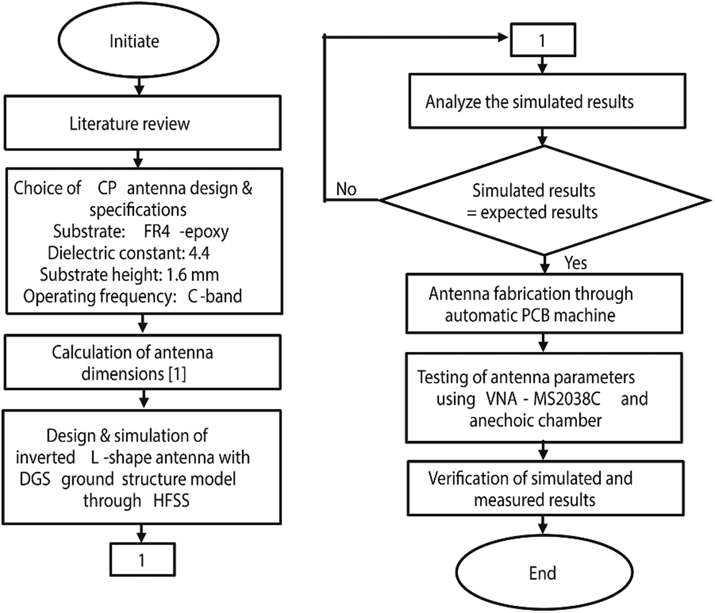
Fig. 1. Flowchart of antenna design steps.

Fig. 2. Geometry of top view (orange color) and bottom view (red color) of the proposed antenna.
In this work, the performance of the five different antenna designs (A1 – A5) is investigated and the antenna design (A5) is selected for C-band applications based on the simulated results closest to design considerations. The geometrical configuration of the proposed antenna (A5) and photographs of the proposed antenna after fabrication are presented in Fig. 2 and Figs 3(a) and 3(b), respectively.

Fig. 3. Photograph of the proposed antenna after fabrication: (a) top view (b) back view.
Evolution of the proposed structure
The effect of stub and antenna performance is presented in Figs 4 and 5, respectively. To optimize the antenna parameters, the ground plane structure of antennas A1 – A5 (cf. inset of Fig. 5(a)) has been modified and simulated to observe the behavior of inner square track, slits, notch, and stub/perturbation. Antenna A1 is obtained by removing a square track of (26 × 26 mm2) from the ground plane and a square-shaped slot (24 × 24 mm2) is removed from the ground of antenna A1 to get antenna A2. The geometry of antenna A3 is obtained by introducing the slits of (1 × 24 mm2) along with the x-axis of the ground plane of antenna A2. This geometry creates an electromagnetic coupling gap at the inner ground. Further, antenna A4 is obtained by creating a notch (3 × 2 mm2) onto the upper part of the inner ground of antenna A3. Finally, the proposed antenna A5 (cf. Fig. 2 and inset of Fig. 5(a)) is obtained by loading with a perturbation/stub (3 × 8 mm2) in between the slit and left corner of the inner ground of antenna A4.

Fig. 4. Inductive and capacitive effect between stub and proposed antenna.
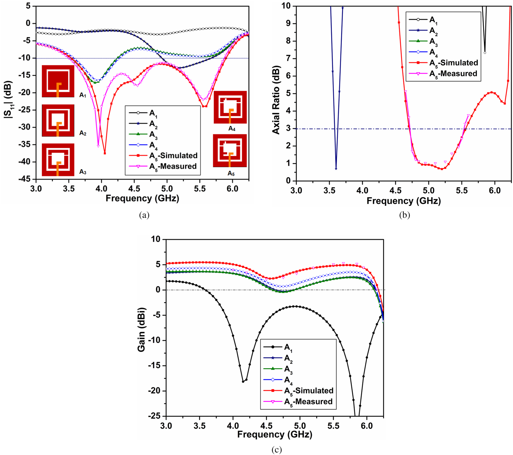
Fig. 5. Parametric analysis of (A1–A5) in terms of (a) return loss, (b) axial ratio, and (c) gain of antenna A5.
Removal of the outer square strip and inner square from the ground plane creates inductive and capacitive loading in input impedance of the proposed antenna respectively (cf. antennas A1 and A2). The additional, capacitive effect is introduced by incorporating slits in design A2, which leads to structure A3. Furthermore, introducing notch and stub on the ground plane changes the electrical behavior of the equivalent lumped element circuit of the proposed antenna. When a notch has been introduced a change in the current length path on the surface of the antenna takes place [Reference Singh, Mishra and Singh30].
The stub primarily governs the center frequency, power loss, and impedance bandwidth of the return loss and axial ratio of the proposed antenna. Due to stub loading, a T-network with an inductor (ΔLs) and a capacitor (ΔC S) is added between the stub and patch equivalent circuits [Reference Mondal, Maity, Ghatak and Bhadra Chaudhuri26]. The elemental values of patch and stub circuit are given after [Reference Mondal, Maity, Ghatak and Bhadra Chaudhuri26, Reference Singh, Mishra and Singh30, Reference Mishra, Singh and Singh31] and values of ΔLs and Cs in terms of patch length (Ls) and stub length (L 2) can be calculated after [Reference Mondal, Maity, Ghatak and Bhadra Chaudhuri26] and given as follows:


The formulation of equations (1) and (2) and represented in Fig. 4 is depicted and compared using return loss |S 11|, exhibited by perturbed psi (ψ)-shaped antenna [Reference Mondal, Maity, Ghatak and Bhadra Chaudhuri26], and the proposed inverted L-shaped antenna (A5) in Fig. 7(a).
After the introduction of the stub, the input impedance of the proposed antenna is changed significantly and matches the characteristics of feed-line impedance (50 Ω). The effect of the stub on return loss and the axial ratio is presented in Figs 5(a) and 5(b), respectively. In Fig. 5(a), a better-simulated impedance bandwidth (2.39 GHz) and return loss (−37.12 dB) for the proposed antenna-A5 (with stub) are observed as compared with the impedance bandwidth (0.72 GHz) and return loss (−16.4 dB) for antenna-A4 (without stub). Figure 5(b) demonstrates that the 3-dB axial bandwidth is achieved only for antenna-A2 and the proposed antenna-A5 with 3-dB axial bandwidth of 0.03 and 0.84 GHz, respectively, and no usable bands are obtained in C band for antennas A1, A3, and A4 (cf. Table 2).
Table 2. Performance analysis of antenna shape A1, A2, A3, A4, and A5.

S – simulated, M – measured, and A5 – proposed antenna.
The performance in terms of return loss, axial ratio, and 2D gain of antennas A1 – A5 is investigated and presented in Figs 5(a)–5(c), respectively. Simulated results of antennas A1, A2, A3, A4, and A5 are tabulated in Table 2. Antenna A1 does not offer any usable −10 dB emission band (S 11 <−10 dB), −3 dB axial ratio band and gain. In antenna A2, we observe −10 dB emission band (4.90–5.66 GHz) and −3 dB axial ratio band (3.6–3.63 GHz) but with a narrow bandwidth (0.76 GHz) and a narrow ARBW (0.03 GHz) in different regions of C band (cf. Figs 5(a) and 5(b)).
Antennas A3 and A4 are resonating in bands (3.54–4.21 and (3.54–4.21 GHz), respectively, (cf. Fig. 5(a)) with an improved gain (3.38 dBi) but no usable axial band is observed. In antenna A5, large −10 dB bandwidth (2.39 GHz) (cf. Fig. 5(a)) and ARBW (0.84 GHz) (cf. Fig. 5(b)) and improved 4.92 dBi (−10 dB band) and 5.08 dBi (3 dB axial band) gain (cf. Fig. 5(c)) is observed, respectively, without sacrificing the performance of other antenna parameters.
Antennas A3 and A4 are resonating in bands (3.54–4.21 and (3.54–4.21 GHz), respectively, (cf. Fig. 5(a)) with an improved gain (3.38 dBi) but no usable axial band is observed. In antenna A5, large −10 dB bandwidth (2.39 GHz) (cf. Fig. 5(a)) and ARBW (0.84 GHz) (cf. Fig. 5(b)) and improved 4.92 dBi (−10 dB band) and 5.08 dBi (3 dB axial band) gain (cf. Fig. 5(c)) is observed, respectively, without sacrificing the performance of other antenna parameters.
Results and discussion
The performance of the optimized proposed antenna (A5) in terms of S 11-parameter, axial ratio, gain, surface current density, and radiation pattern has been carried out in this section. Based on the parametric analysis of antenna shape as discussed in the preceding sections, antenna A5 is chosen as the optimum design for fabrication.
A comparative overview of reported CP antennas and the proposed antenna for C-band applications in terms of antenna size, operating band, percentage bandwidth, 3-dB axial ratio band, and ARBW, gain, and used substrate is presented in Table 1. It is established from the perusal of Fig. 6 that the total area of the proposed antenna (1024 mm2) is less by a factor of 7.45, 2.71, 1.97, and 9.76 as compared to the antennas reported in [Reference Bairami and Zavvari25] (8100 mm2), [Reference Mondal, Maity, Ghatak and Bhadra Chaudhuri26] (2776 mm2), [Reference Maddio27] (2025 mm2), [Reference Li, Zhang and Feng28], and (10 000 mm2), respectively, whereas greater than that of the antenna [Reference Ashraf, Tahir and Abbasi29] (800 mm2) by a factor of 1.28.

Fig. 6. Antenna size (mm2) of the proposed and reported antennas.
The proposed antenna has been fabricated on the FR4 substrate and parameters are measured using a vector network analyzer (MS2038C) (cf. inset of Fig. 7(c)) and test antenna placed in situ in an anechoic chamber (cf. Fig. 10). Reported in [Reference Bairami and Zavvari25–Reference Ashraf, Tahir and Abbasi29] and the proposed antenna's measured return loss have been compared and plotted in Fig. 7(a) and the associated parameters are tabulated in Table 1.
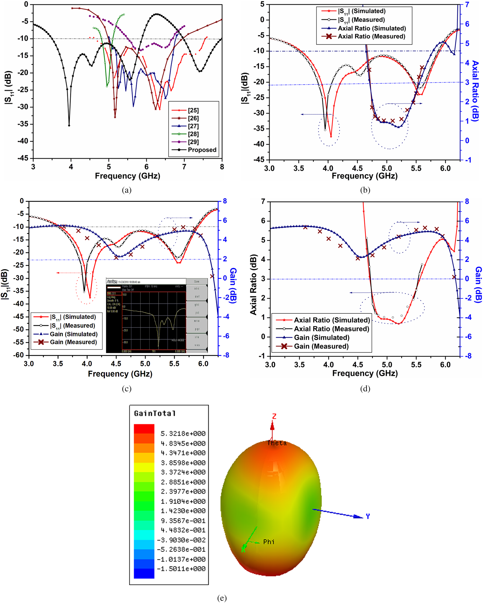
Fig. 7. (a) Comparative return loss plot of proposed and previously reported antennas, (b) return loss and axial ratio plot, (c) return loss and gain plot, (d) axial ratio and gain plot, and (e) 3D gain of antenna A5.
Simulated and measured return loss |S 11| and the axial ratio of the proposed antenna are illustrated in Fig. 7(b). The proposed antenna achieves 50.6% measured −10 dB (S 11 <−10 dB) impedance bandwidth (cf. Figs 7(a) and 7(b)) which is larger than the antennas reported in Table 1 [Reference Bairami and Zavvari25–Reference Ashraf, Tahir and Abbasi29] by 3% [Reference Bairami and Zavvari25], 10.9% [Reference Mondal, Maity, Ghatak and Bhadra Chaudhuri26], 21.9% [Reference Maddio27], 45.1% [Reference Li, Zhang and Feng28], and 31.7% [Reference Ashraf, Tahir and Abbasi29], respectively.
Due to loading of the stub, we observe (cf. Figs 5(a), 7(a) and 7(b), Table 1) a fairly wide bandwidth in case of perturbed psi (ψ)-shaped antenna [Reference Mondal, Maity, Ghatak and Bhadra Chaudhuri26] and the proposed inverted L-shaped antenna (A5). However, 16.2% ARBW is observed in Fig. 6(b) which is greater than the antennas [Reference Maddio27–Reference Ashraf, Tahir and Abbasi29] by 0.7, 10.2, and 1.8%, but smaller than the antennas [Reference Bairami and Zavvari25, Reference Mondal, Maity, Ghatak and Bhadra Chaudhuri26] by 25.8 and 3.2%, respectively. In comparison to reported antennas [Reference Bairami and Zavvari25–Reference Ashraf, Tahir and Abbasi29], better-measured return loss (−35.5 dB) is observed in the case of the proposed antenna (cf. Fig. 7(a)).
Figure 7(c) illustrates that the antenna gain is stable (5.3 dBi) in the entire frequency band (3.48–5.86 GHz) except at 4.54 GHz. Due to a ringing phenomenon (multiple resonant peaks occurring in the operating band) (cf. Figs 7(a)–7(c)) and antenna losses, we observe unstable gain (cf. Fig. 7(c)) in the ringing zone (4.0–5.4 GHz) as reported in [Reference Singh, Mishra and Singh32].
We observe an almost stable gain till 4.0 GHz. After 4.0 GHz it starts degrading and continues to degrade till the 4.55 GHz and thereafter, the gain starts improving (cf. Fig. 7(c)). Degradation of gain is attributed due to the ringing phenomenon and it conforms with the earlier findings as reported in [Reference Singh, Mishra and Singh32]. Interestingly, as the gain starts improving (≈4.55 GHz), we observe the emergence (start point) of the axial ratio band which is terminating at 5.54 GHz, the point from where the gain again starts degrading (cf. Fig. 7(d)). A measured 5.3 dBi (at 5.65 GHz) and 5.1 dBi (at 5.49 GHz) peak gain is observed in −10 dB band (3.48–5.86 GHz) and 3 dB axial ratio band (4.71–5.54 GHz), respectively. Simulated 2D and 3D gains of the proposed antenna are presented in Figs 7(c)–7(e) and agree with each other.
A better gain (6.25 dBi) and ARBW (42%) reported in [Reference Bairami and Zavvari25] as compared to the gain (5.35 dBi) and ARBW (16.2%) for the proposed antenna can be attributed due to the thickness of the substrate (T proposed−1.6 mm > T R−25,−0.8 mm). However, the impedance bandwidth (50.9%), antenna size (0.54λ 0 × 0.54λ 0), and return loss (−35.4 dB) of the proposed antenna are significantly better than the impedance bandwidth (47.9%), antenna size (1.87λ 0 × 1.87λ 0), and return loss (−30 dB) for the antenna reported in [Reference Bairami and Zavvari25]. Reported in [Reference Bairami and Zavvari25–Reference Ashraf, Tahir and Abbasi29] and proposed antennas show variation in their measured return loss, operating bands, impedance bandwidths, ARBW, and gains which are largely due to the different design parameters and substrate materials used.
The marginal deviation of 100 MHz is observed between the first simulated (4.05 GHz; S11: −37.5 dB) and measured (3.95 GHz; S11: −35.4 dB) resonant frequencies with not a significant difference in the return loss (cf. Figs 7(b) and 7(c)). However, at the second resonant peak (5.56 GHz) we observe an almost negligible difference between simulated and measured resonant frequencies as well as very little difference between simulated (−23.9 dB) and measured (−21.9 dB) return losses (cf. Figs 7(b) and 7(c)). Deviations observed are due to the tolerance in measuring instruments, dielectric, and conductor losses, impedance mismatch arising out of soldering of SMA connector and connecting probe.
Simulated surface current density distributions at the ground plane (magenta arrow) in the – Z-direction and the radiating patch (black arrow) in the + Z-direction at the axial resonant frequency of 5.1 GHz is presented in Fig. 8. In the + Z-direction, a clockwise rotation of current distribution corresponds to left-hand CP (LHCP), and counter-clockwise rotation refers to right-hand CP (RHCP) with the advancement of 90° phase shift and vice-versa in the – Z-direction. A counter-clockwise rotation (RHCP) on the radiating patch (black arrow) and clockwise rotation (RHCP) on the ground plane (magenta arrow) with 90° phase shift during 0°–270° is observed in Fig. 8. From the perusal of Fig. 8, it is concluded that the proposed antenna presents RHCP in the axial ratio band (4.71–5.54 GHz), and rotation of the ground plane (clockwise) and radiating patch (counter-clockwise) verify CP.

Fig. 8. Simulated surface current distribution at 5.1 GHz frequency for 0°, 90°, 180°, and 270°.
It has been observed in Fig. 8 that at 0° and 180° phase shift, the maximum current is flowing from left to right and right to left along with the x-axis on the inverted L-shaped patch, respectively. However, at 90° and 270° phase shift, maximum current is flowing in the upward and downward directions along with the y-axis on the radiating patch, respectively. At 5.1 GHz, surface current density and its direction on the radiating patch demonstrate that the antenna is operating in TM10 mode at 0° and 180° and TM01 at 90° and 270° phase shift.
Far-field simulated and measured radiation patterns of the proposed antenna at 5.1 GHz are shown in the x–z-plane (ϕ = 0°) and the y–z-plane (ϕ = 90°), as shown in Figs 9(a) and 9(b), respectively. To illustrate the direction of CP, both LHCP and RHCP patterns are plotted. The CP behavior of the proposed antenna is the same in the x–z and y–z planes at 5.1 GHz. The difference between the magnitude of LHCP and RHCP is in the acceptable range and the RHCP component is larger than the LHCP component at 5.1 GHz. The CP behaviors of Figs 8 and 9 are in consonance and confirm the RHCP waves of the proposed antenna. The measurement setup of the proposed antenna in an anechoic chamber is presented in Fig. 10.
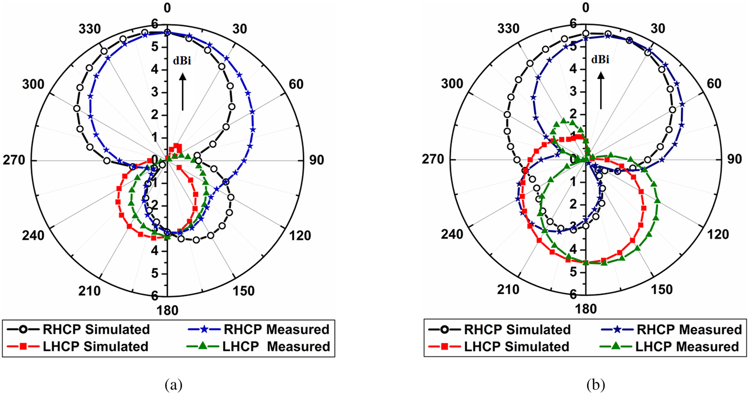
Fig. 9. Simulated and measured radiation patterns at 5.1 GHz: (a) the x–z-plane and (b) the y–z-plane.

Fig. 10. Measurement setup of the proposed antenna in an anechoic chamber.
Conclusions
A low cost and compact inverted L-shaped CP antenna for C-band applications is designed with 16.9% fractional bandwidth (S 11<−10 dB) and 16.2% ARBW (3 dB axial ratio). The introduction of the stub on the ground plane reduces the power loss of the proposed antenna and enhances the bandwidth. A large bandwidth (2.39 GHz) and good return loss (−37.12 dB) are observed with the introduction of the stub as compared to the bandwidth (0.72 GHz) and return loss (−16.4 dB) of the antenna-A4 without the stub.
The proposed antenna has been designed using a very low cost of the epoxy laminate material (FR4), exhibiting a fairly large impedance bandwidth (50.9%), and a reasonably good peak gain (5.35 dBi). However, it is rather difficult to achieve large bandwidth and gain simultaneously [Reference Mishra, Singh and Singh33], but in the proposed antenna, when a stub is introduced, we observe rather a nearly perfect trade-off between these two parameters which is a hallmark of the proposed design.
In future, the proposed antenna design can be tested for different applications covering more frequency bands either by implementing it by using an array of antennas or by using meta-materials and other substrate materials [Reference Jain, Kanaujia, Dwari, Pandey and Singh34] with varying heights and dielectric constants.
 Mr. Karunesh Srivastava received his B.Tech. degree in Electronics & Communication Engineering from Uttar Pradesh Technical University Lucknow, M.Tech. degree in Electronics Engineering Department from University of Allahabad, Prayagraj. He is currently pursuing his research work for his Ph.D. degree from the University of Allahabad, Prayagraj, UP, India. He has published more than 14 research papers in journals of international repute, international conferencesand book chapters. His current research interests include microwave filters, planar, and reconfigurable antennas.
 Dr. Brijesh Mishra received his M.Tech. (Electronics Engineering) and D.Phil. (RF and Microwaves) degrees from the University of Allahabad in 2012 and 2018. Dr. Brijesh Mishra worked as an Assistant Professor in the Department of Electronics and Communication Engineering at Shambhunath Institute of Engineering and Technology (SIET) during 2012–2013 and 2017–2018. Presently, he is working as an Assistant Professor (NPIU-MHRD) in the Department of Electronics and Communication Engineering at the Madan Mohan Malaviya University of Technology. He has published more than 35 research papers in journals of international repute, international conferences, and book chapters. He is the principal investigator and co-investigator in two NPIU and World Bank-funded projects. He is the recipient of awards like Excellence in Performance and Outstanding contributions. He has served as Organizing Track Chair and Organizing Secretary in IEEE Conference (ICE3–2020) and Springer Conference (ICVMWT-2021), respectively. He is a member of IEEE, ISTE, IE(I), IETE, IAENG, and IFERP. His research interest includes modelling, simulation, and fabrication of RF and microwave devices and their applications.
 Dr. Rajeev Singh received his B.Tech. (Electronics and Telecommunication) and M.Tech. (Electronics Engineering) degrees from the University of Allahabad in 1992 and 1994. He received the DAAD (Deutscher Akademischer Austausch Dienst-German Academic Exchange Service) in 2003 and worked for his Ph.D. degree in the Institute for Physics and Astronomy, Potsdam University, Germany and he again visited the Federal Republic of Germany in 2008. Participated in Meetings of Nobel Laureates in Lindau, Germany in 2004. He has more than 24 years of teaching and research experience. At present, he is a Professor and Head of the Department of Electronics and Communication, University of Allahabad. He has published more than 65 research papers in journals of international repute, international conferences, book chapters, etc. He has successfully supervised doctoral thesis leading to the award of degree to four students. He has served as an expert reviewer of different international journals in the field of antenna and microwave engineering. He has also served in various capacities such as member Board of Studies, Faculty Board, Academic Council, Director Administrative Computer Centre, the Chairman undergraduate admission committee at the University of Allahabad. He has also served as an expert member in various selection committees of the Universities and Public Service Commission. His current interest in research areas is micro-strip antenna, microwave engineering, microwave filters, polymer electronics, and soft matter.


