


I. INTRODUCTION
Traditionally, there are two methods used for electrically controlled rectangular waveguide switches at high frequencies. Either an electrical motor is utilized to break the waveguide path with a rotating block [Reference Kich and Ando1] or a p-i-n diode is incorporated inside the waveguide acting as a switch [Reference Henry, Heitzmann and Sillard2, Reference Craven3]. Motors are heavy and bulky in comparison to p-i-n diodes, which, however, exhibit poor radio frequency (RF) performance.
RF microelectromechanical systems (RF MEMS) allow for creating highly integrated reconfigurable geometries interacting with RF and microwave signals, and can also be utilized to interfere with wave propagation in a waveguide. Such a concept benefits from general advantages of RF MEMS devices such as excellent RF performance, very small size, fast response, and high-volume manufacturability [Reference Rebeiz4–Reference Lucyszyn6]. RF MEMS devices demonstrated so far include switches [Reference Rebeiz and Muldavin7–Reference Mahameed and Rebeiz11], tunable capacitors [Reference Nieminen, Ermolov, Nybergh, Silanto and Ryhänen12–Reference Borwick, Stupar, DeNatale, Anderson, Tsai, Garrett and Erlandson14], phase shifters [Reference Lakshminarayanan and Weller15–Reference Somjit, Stemme and Oberhammer17], three-dimensional micromachined inductors, and transmission lines [Reference Jiang, Wang, Yeh and Tien18–Reference Hong-Teuk, Sanghwa, Jae-Hyoung, Chang-Wook, Yong-Kweon and Youngwoo20].
To the knowledge of the authors, the Ku- and K-band waveguide switch presented by Daneshmand et al. [Reference Daneshmand, Mansour and Sarkar21] is the only publication which attempted using MEMS for waveguide switching. Here, MEMS electrothermal actuators have been integrated with a ridge waveguide to construct the switch. For this switch, a return loss of better than −15 dB, insertion loss of 1–2.8 dB and an isolation of better than 15 dB was achieved for frequencies below 30 GHz.
Table 1 summarizes the performance of some high-frequency commercial electrically controlled rectangular waveguide switches, and the MEMS waveguide switch presented by Daneshmand et al. [Reference Daneshmand, Mansour and Sarkar21].
Table 1. Examples of electronically controlled rectangular waveguide switches.

In this paper, we introduce a novel RF MEMS waveguide switch utilizing up to 1260 reconfigurable cantilever elements with up to 660 simultaneously switched contact points for short-circuiting the electric field lines of the TE10 mode of a rectangular waveguide. The MEMS waveguide switch is only 30 µm thick, supported by a 500 µm substrate which is inserted into the cross-section of a standard WR-12 waveguide.
II. CONCEPT AND ELECTROMAGNETIC DESIGN
Figure 1 shows a schematic of the proposed MEMS waveguide switch in both ON- and OFF-states. The reconfigurable surface is implemented in a WR-12 rectangular waveguide (3.099 mm × 1.549 mm) and consists of two sets of micromachined vertical contact cantilevers separated at every other line in the horizontal direction as shown in Fig. 1(a). The first set of contact cantilevers is fixated and the second set is movable synchronously in the horizontal direction. When the switch is in the ON state, as shown in Fig. 1(b), there is a gap between the fixated and moveable set of cantilevers which allows the wave to propagate freely through the reconfigurable surface, which is transmissive in this state. When the switch is in the OFF-state, as shown in Fig. 1(c), the movable set of contact cantilevers are laterally displaced by integrated MEMS actuators to short-circuit the electric field lines of the predominant TE10 mode. In this case, the wave propagation is blocked, i.e. the reconfigurable surface is total-reflective.

Fig. 1. Concept of novel MEMS waveguide switch: (a) cross-section of switch drawn for 3 moving and 2 fixed horizontal suspension bars and 10 cantilever columns (resulting in 60 contact points and 100 cantilevers); (b) ON-state (non-blocking), and (c) OFF-state (blocking) of waveguide switch.
The number of contact cantilevers can be optimized for achieving good RF performance both in the ON- and in the OFF-states, as a large number of vertical cantilevers increases OFF-state isolation but also affects ON-state insertion loss negatively.
A) Effect of short-circuiting bars on RF performance
The contact cantilevers are distributed uniformly in the waveguide. The number, i.e. density, of short-circuiting bars is expected to have an influence both on the isolation of the switch in the OFF-state, as well as the insertion loss in the ON-state.
The basic HFSS-simulation finite element model with a varying number of vertical short-circuiting bars is shown in Fig. 2(a). The width and thickness of the vertical bars are 50 and 30 µm, respectively. For simplifying the model, the bars have been modeled as completely filled gold blocks including metal losses (conductivity of 41 MSm−1). Simulation results for a number of vertical short-circuiting bars from 5 to 30 are shown in Figs 2(b) and 2(c).

Fig. 2. Basic simulation model to investigate the effect of the number of vertical bars on RF performance: (a) HFSS model; (b) S11 simulation results; and (c) S21 simulation results.
For this blocking configuration, it can be seen that the reflected power S11 is better than −0.05 dB and the isolation S21 is better than −23.5 dB for structures with more than 10 vertical bars, i.e. only a total blocking area of 16% of the waveguide cross-section is needed for achieving sufficient blocking of wave propagation. It is not the fill-factor which determines the isolation but rather the density of the vertical bars as compared to the field distribution in the waveguide.
B) Design with reconfigurable surface
For the reconfigurable surface, the vertical bars are split into smaller sections (cantilever pairs), and mechanically connected via horizontal suspension bars. The movable vertical cantilevers are designed to be laterally displaced by having their horizontal suspension bars connected to MEMS actuators, as shown in Fig. 1(a). Since the horizontal suspension bars are perpendicular to the electric field inside the waveguide, they have a negligible effect on RF performance of the structure even in the ON-state.
For the implemented designs, the width and thickness of the contact cantilevers are 5 and 30 µm, respectively. The overlap between the contact cantilevers in the OFF-state is 5 µm.
An HFSS model of the structure, with varying number of vertical cantilever columns and horizontal suspension bars, was set up as shown in Fig. 3. The reconfigurable surface is modeled with filled gold bars, including metal losses. The simulated S-parameters of the model, for four different configurations whose parameters are summarized in Table 2, are presented in Fig. 3. The designs A and B have 20 vertical cantilever columns, whereas the designs C and D utilize 30 columns. The number of horizontal suspension bars is 21 for designs B and D, and 9 and 17 for A and C, respectively. This results in a total number of parallel contact points of up to 660 for design D with 1260 cantilevers. Designs B–D achieve good simulated performance with reflected power S11 better than −0.04 dB and an isolation better than 24 dB in the blocking state, and a return loss of S11 better than −25 dB, and an insertion loss better than 0.08 dB for the transmissive state. It can be concluded that design B, with 21 horizontal suspension bars and 20 vertical cantilever columns, shows the best performance of these four designs in the ON-state; when designs D and C, with 30 vertical cantilever columns, are in the OFF-state.

Fig. 3. Complete HFSS simulation model of the reconfigurable surfaces, including all moveable cantilevers, suspension bars, and mechanical feedthroughs for the MEMS actuators, and S-parameter simulation results for the blocking and non-blocking states, for 4 basic designs A–D.
Table 2. Summary of design parameters of designs A–D.

Figure 4 shows the simulated RF performance of the novel waveguide switch with different number of horizontal suspension bars and vertical cantilever columns at 75 GHz. In the OFF-state (blocking), increasing the number of vertical columns blocks wave propagation better and improves performance noticeably while increasing the number of horizontal suspension bars has a small effect. However, in the ON-state (non-blocking), increasing the number of vertical cantilever columns degrades the performance due to increased blocking of wave propagation due to increased total capacitance in the waveguide, while increasing the number of horizontal suspension bars improves the performance. Increasing the number of horizontal suspension bars increases the number of contact cantilevers in each column, thus decreasing the total effective capacitance made by series combination of these capacitances in the non-blocking, i.e. transmissive, state.
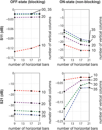
Fig. 4. Effect of number of vertical cantilever columns and horizontal suspension bars on RF performance, from ANSYS HFSS simulation of Fig. 3, extracted at 75 GHz.
III. ACTUATOR DESIGN AND PROTOTYPE FABRICATION
MEMS electrostatic comb-drive actuators [Reference Legtenberg, Groeneveld and Elwenspoek22, Reference Hou, Huang, Huang, Liao, Chen and Yeh23] with folded beam springs are placed on the same chip but outside the waveguide wall to move the contact cantilevers as shown in Fig. 1(a). The design is based on push–pull actuators and it is required to displace the contact cantilevers by a total of 25 µm to switch between the ON-state (transmissive, non-blocking) and the OFF-state (reflective, blocking) states. COMSOL multiphysics simulations resulted in design of three different actuators with spring constants of 2.21, 4.36, and 7.83 N/m and nominal actuation voltages of 50, 71, and 90 V, respectively.
The micromachining process flow of the waveguide switch, fabricated on a silicon-on-insulator (SOI) wafer with RF MEMS process which was developed by the authors [Reference Sterner, Roxhed, Stemme and Oberhammer24], followed by an additional back-etching process of the handle wafer, is summarized in Fig. 5. The elements of the reconfigurable surface, the suspension cantilevers, and the MEMS actuators are fabricated in the same process.

Fig. 5. Outline of fabrication flow of the MEMS waveguide switches, based on deep reactive ion etching from both sides of a silicon-on-insulator wafer, free-etching of the moveable parts and subsequent metallization.
Microscope photographs and a SEM picture of a fabricated chip are shown in Fig 6. The movable contact cantilevers are connected to a shuttle by the use of horizontal suspension bars and vertical grid structures parallel to the narrow wall of the waveguide. Applying an actuation voltage to the comb drives displaces the whole shuttle, which results in the displacement of the structure in direction parallel to the wider walls of the waveguide.
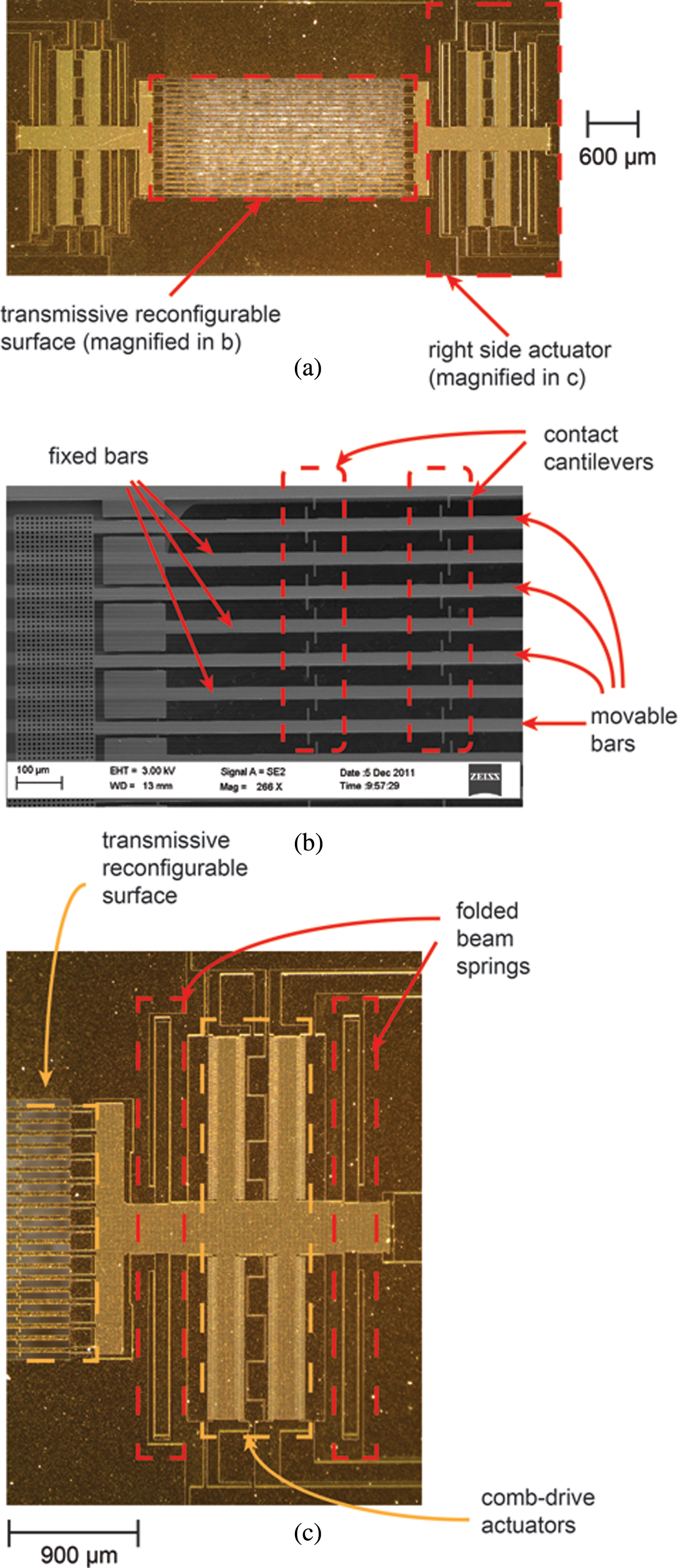
Fig. 6. Pictures of a fabricated prototype device: (a) microscope image of full chip including the reconfigurable surface in the middle and the MEMS actuators at the sides; (b) SEM image of magnified part of central reconfigurable surface; (c) microscope image of MEMS actuators on the right side of the waveguide reconfigurable surface including four-folded beam springs and two stages of comb-drive actuators.
IV. WAVEGUIDE INTEGRATION
A special section of a WR-12 rectangular waveguide flange, shown in Fig. 7, is fabricated for integrating the chips into the waveguide. The chip is fixated in the recess of a bottom waveguide flange and a double-side adhesive, compliant, and conductive polymer sheet (Ted Pella Silver Conductive Sheet 16086; nominal thickness of 125 µm; resistivity of 8 mΩcm) is applied on the front side of the chip before closing the top flange.

Fig. 7. Integration of the micromachined chips into a standard WR-12 waveguide: (a) assembled measurement setup; (b) schematic drawing and simulation model of different assembly parts, including modified waveguide flanges, an intermediate fixating device, and a prototype chip with conductive polymer interposers.
Utilizing the conductive polymer sheet in the assembly has numerous advantages. The main advantage is to provide electrical conductivity by filling the gap between the waveguide wall and the chip surface to decrease the loss, primarily by not interrupting the surface currents on the waveguide walls. In addition, the softness of the polymer allows for securely bonding the chip to the waveguide for a reliable mechanical connection, as it addresses the mismatch between macroscopic surface roughness of the precision-machined rectangular waveguide surface and the nanometer-scale surface roughness of the MEMS chip, by the soft interposer layer which drastically reduce the risk of breaking the brittle MEMS chip at local stress contact points. Furthermore, as this assembly method is non-permanent, it facilitates interchange of the MEMS chips for testing and calibration purposes.
Finite Element Method (FEM) simulations of the assembly concept were carried out in CST Microwave Studio, to show the performance improvement and design robustness of utilizing the conductive polymer sheet over the conventional air-gap interface.
In order to facilitate mechanical feedthroughs in the waveguide frame on chip, the effect of an opening in a waveguide wall was investigated. Figures 8(a) and 8(b) show simulation results investigating the influence of an air-gap in a waveguide junction, for different gap sizes and two different cases: gap between two WR-12 waveguides surrounding the whole waveguide circumference, and a gap only between the narrow walls. A gap on the whole circumference has a drastic effect on the loss even for distances as small as 50 µm. However, if an air gap exists only between the narrow walls of the waveguide, it has less influence on the performance even up to a gap of 500 µm in a WR-12 waveguide, as the wide waveguide walls are primarily carrying the surface currents.

Fig. 8. Simulated influence of air gaps between two WR-12 waveguides: (a) air gap around the whole circumference of the waveguide; (b) air gap only on the narrow sides of the waveguide.
Figure 9 shows the simulated performance of the assembly with a conductive polymer with parameter variation of the polymer sheet thickness. Also here two different cases, with the interposer layer covering all walls of the waveguides or only the wide walls, are investigated. When the conductive polymer is covering only the wide walls, a polymer thickness of up to 1.5 mm is degrading insertion loss only to about 0.44 dB over the whole E-band. Applying the conductive polymer on all walls of the waveguide improves the insertion loss to 0.2 dB for the same variation range. For a polymer layer thickness of 100 µm as used in this paper, the simulated insertion loss for both cases below 0.02 dB, is negligible.

Fig. 9. Simulated interface performance between two WR-12 waveguides with conductive polymer as interposer layer, with polymer thickness as parameter, for two cases: conductive polymer connecting only the wide walls of the waveguide, and conductive polymer ring around the whole circumference of the waveguide.
A simulation model for the complex chip assembly setup, as shown in Fig. 7, was created in CST Microwave Studio, considering both metal and dielectric losses, and the simulation results are shown in Fig. 10. Here, the influence of the polymer interposer is investigated, and compared to an ideal direct waveguide-to-chip connection. The polymer layer in the connection has near-ideal performance, and for polymer thickness in the order of 120 µm there is no significant difference between having the polymer interposer only on the wide sides of the waveguide, or along the whole waveguide circumferences.

Fig. 10. Simulated performance of the assembled microchip-in-waveguide setup shown in Fig. 7(b), for a polymer interposer only on the wide sidewalls of the waveguide, as utilized for device assembly in this paper, and with polymer interposer around the whole circumference of the waveguide, compared to an ideal direct waveguide to chip connection.
Figure 11 shows the measured performance of complete assembly setup with a dummy chip, i.e. a chip not containing the reconfigurable surface, measured for an assembly with the conductive polymer sheet and an assembly without the sheet. The assembly without the polymer interposer most probably results in an unavoidable, partial air gap. The measurements show that utilizing the conductive polymer interface improves the performance and results in stable measurements over the whole frequency range. The insertion loss of the whole assembly setup, including the conductive polymer interface is less than 0.5 dB for 60 GHz.

Fig. 11. Measured performance of complete assembly setup, including the two modified waveguide flanges, and a reference microchip without a reconfigurable surface as shown in Fig. 7(a). The measurement with the polymer interposer gives much more stable results than without the polymer, as the latter case might lead to partial air gaps between the chip and the waveguide.
V. EXPERIMENTAL CHARACTERIZATION OF RECONFIGURABLE SURFACES
As analyzed in Section 2, for providing good isolation in the OFF-state (blocking waveguide switch, i.e. the switches of the surfaces are closed), the most important design parameter is the number and distribution of vertical cantilever columns. For the ON-state, however, in addition to the number of vertical cantilever columns, the distribution and number of gaps between the non-touching cantilevers are important which is designed by the number of horizontal suspension bars.
Figure 12 shows the RF measurement results of prototypes of the four designs, whose parameters are summarized in Table 2, including the presented chip-to-waveguide assembly based on two modified flanges and the polymer interposer which is only applied between the top of the chip and wide side of the waveguide. The overall performance in comparison to the simulation is compromised by loss of the assembly setup alone, which can be seen from the reference measurement (chip without reconfigurable surface in assembled setup) which is included in Fig. 12. In the ON-state, the measured overall insertion loss (Fig. 12(d)) is better than 0.8 dB for design A and C, and better than 1.2 dB for designs B and D, for 60–70 GHz. The measured return loss of the switch in the ON-state (Fig. 12(b)) is better than 15 dB for designs A, C, and D, and better than 20 dB for design B up to 68 GHz. In the OFF-state, the measured isolation (Fig. 12(c)) is better than 30 dB for all designs. The measured reflected power in the OFF-state (Fig. 12(a)) is between 0.2 and 1.8 dB for the spectrum but inconsistent, most probably due to calibration difficulties of the complex waveguide assembly setup. Designs C and D show reflected power of better than −1 dB in the OFF-state.

Fig. 12. S-parameter measurement results of prototypes of the MEMS waveguide switches of designs A–D, including complete assembly setup, with a reference measurement with a reference chip not containing any reconfigurable surface.
Unfortunately, the MEMS comb-drive actuators did not properly actuate for the expected (simulated) actuation voltages of 50 V due to poor fabrication yield of the narrow and long mechanical springs. Therefore, for measuring the prototype samples in the OFF-state, the devices were fixated mechanically. The two major problems associated with the prototype fabrication run were over-etching of the mechanical springs in the deep silicon etching step and stiction after the critical point drying step. It is believed that both problems can be solved by design, in particular by improving the stability of the comb-drive actuators by having stiffer springs in-plane and in out-of-plane direction. Nonetheless, the RF measurement results of the mechanically fixated test devices are in good agreement with the simulation which supports the proof of concept.
VI. CONCLUSION
This paper reported on design, fabrication, and evaluation of a novel concept of a MEMS waveguide switch based on a reconfigurable transmissive surface of a thickness of only 30 µm, consisting of up to 1260 simultaneously reconfigurable cantilevers and 660 electrical contact points, and integrated into a conventional WR-12 waveguide. Unfortunately, the devices could not be actuated mechanically at the designed voltages and the characterization was performed in the fixated position. The measurement results of these novel waveguide switches show that the fabricated prototypes are clearly able both to block propagation in the OFF-states with over 30 dB isolation for all designs, and allow transmission with less than 0.65 dB insertion loss for the best design in the ON-state in the V-band. The simulated performance is even better, and the discrepancy between the simulation and measured results is mainly attributed due to the complexity of the chip-to-waveguide assembly which has been demonstrated by reference measurements.
ACKNOWLEDGEMENT
The research leading to these results has partly been funded from the European Community's Seventh Framework Programme under grant agreement n°267528 (xMEMS, grant holder: Göran Stemme).
 Zargham Baghchehsaraei was born in Tehran, Iran, in 1982. He received the B.S. degree in Electrical Engineering from Iran University of Science and Technology, Tehran, Iran, in 2006, and the M.S. degree in Electrical Engineering with emphasis on microsystem technology from Chalmers University of Technology, Gothenburg, Sweden, in 2009. Since 2009, he has been working toward a Ph.D. degree in the Micro and Nanosystem (MST) group, KTH Royal Institute of Technology under the supervision of Dr. Oberhammer. His research focuses include Microwave and RF-MEMS based switches, filters, and antenna arrays.
 Umer Shah was born in 1981 in Pakistan. He received his B.S. degree in Engineering from GIK Institute, Pakistan in 2003. After working at GIK Institute as a Researcher for one year, he went to pursue his Masters from Technical University of Denmark (DTU) in 2004. In 2007, he completed his Master of Science degree in Wireless Engineering with emphasis on RFIC, MMIC, and Antenna design. He worked with Interactive Sports Games (ISG) A/S for his Masters thesis. After his Masters degree, he worked on developing satellite front ends at a research organization. Since December 2008, he has been a Ph.D. student in the MST group under the supervision of Dr. Joachim Oberhammer. His research focuses includes RF MEMS-based filters, phase shifters, matching circuits, and antennas. His further interests includes MMIC, RFIC, and Antenna Design. He was the recipient of the Best Student Paper Award presented at the Asia Pacific Microwave Conference 2010, Yokohama, Japan.
 Jan Åberg started with microwave work 1973 at SATT, in 1975 he joined the start-up company IMA and doing very stable, and fast hopping oscillators. In 1983, he joined Ericsson and more specifically the electronic warfare group. There, he worked in both R/D and program management until he became an advisory engineer in microwave design, later the group became part of the SAAB group. In 2005, he and a fellow started MicroComp Nordic AB where he still works.
 Göran Stemme received the M.Sc. degree in Electrical Engineering and the Ph.D. degree in solid-state electronics from Chalmers University of Technology, Gothenburg, Sweden, in 1981 and 1987, respectively. In 1981, he joined the Department of Solid State Electronics, Chalmers University of Technology, where he became an Associate Professor (docent) heading the silicon sensor research group in 1990. Since 1991, he has been a Professor at KTH Royal Institute of Technology, Stockholm, Sweden, where he heads the Microsystem Technology Laboratory in the School of Electrical Engineering. His research is devoted to microsystem technology based on micromachining of silicon. He has published more than 260 research journals and conference papers and has more than 23 patent proposals or granted patents. He is a member of the Royal Swedish Academy of Sciences (KVA).
 Joachim Oberhammer was born in Italy in 1976, received his Ph.D. degree in 2004 for his work on RF MEMS switches and microsystem packaging. In 2007, he became an Associate Professor at the Royal Institute of Technology where he is heading a research team with activities in RF and microwave MEMS. In 2007, he was a research consultant at Nanyang Technological University, Singapore, and in 2008 he was a guest researcher at Kyoto University, Japan.
He is the author and co-author of more than 80 reviewed research papers and holds 4 patents. In 2004, he received an Ericsson Research Foundation Award and in 2007 a grant by the Swedish Innovation Bridge, respectively. In 2008, he received a scholarship by the Japanese Society for the Promotion of Science. The research work he is heading received the Best Paper Award at the IEEE European Microwave Integrated Circuit Conference in 2009, a Best Student Paper Award at IEEE Asia-Pacific Microwave Conference 2010, an Honorable Mention at IEEE Antenna and Propagation Symposium 2012, and Graduate Fellowships of the IEEE Microwave Theory and Techniques Society (MTT-S) in 2010 and 2011 and of the IEEE Antenna and Propagation Society (AP-S) in 2012. He served as TPRC member of IEEE Transducers 2009, IEEE International Microwave Symposium 2010, 2011, 2012, 2013, and IEEE Micro Electro Mechanical Systems 2011 and 2012. He has been Steering Group member of the IEEE MTT-S and AP-S Chapters Sweden since 2009.


