


I. INTRODUCTION
A major research effort is made to the integration of several functions on the same substrate. Complementary metal-oxide semiconductor (CMOS) integrated circuits have provided an increase in computation speed for several decades [Reference Rebeiz and Muldavin1, Reference Xu and Chowdhury2]. However, the leakage current of the transistor on the off state presents a real limitation for the integration density.
In the other side, the outstanding improvement of microelectromechanical system (MEMS) industrial maturity [Reference Morris wiSpry3, Reference Meindl, Chen and Davis4] makes this technology more and more attractive for reconfigurable systems, such as switching networks, portable wireless systems, phased arrays, low-noise oscillators, and amplifiers [Reference Rebeiz and Muldavin1–Reference Pethica and Tabor5]. This is because of the very low loss and the outstanding linearity of radio frequency (RF)-MEMS capacitors arrays [Reference Rebeiz6, Reference Newman, Ebel, Judy and Maciel7]. There are several examples of devices with excellent performances in the literature [Reference Nishijima, Hung and Rebeiz8–Reference Ke, Miao and Oberhammer14].
One promising concept is to integrate mechanical switches along with transistors, in the aim to achieve zero off-state power dissipation due to zero leakage current of mechanical switches [Reference Newman, Ebel, Judy and Maciel7].
However, the successful integration of mechanical switches into CMOS chips requires the pull-down voltage of RF-MEMS to be decreased under 10 V while still maintaining good contact force in the down-state position, since the contact resistance of the switch is directly proportional to this force based on the simplified Hertz contact model.
One possible solution developed in this paper to achieve high electrostatic force with a low actuation voltage, is to insert a dielectric layer between the actuation electrode and the mobile beam. Indeed, the generated electrostatic force is proportional to the relative permittivity of the media inside the electrostatic gap, as shown in equation (1) [Reference Rebeiz6]:
 $$F_e=\displaystyle{{\varepsilon _r \times \varepsilon _0 \times S \times V^2 } \over {2 \times g{}^2}}\comma \;$$
where F e is the electrostatic force, g is the electrostatic gap, V is the applied voltage, S is the surface of the actuator, ε 0 is the permittivity, and ε r is the relative permittivity.
Figure 1 shows a conceptual device cross-section with and without dielectric layer between the beam and the actuation electrode.

Fig. 1. (a) High actuation voltage with an air-gap (b) low actuation voltage using dielectric layer.
The electrostatic force is directly proportional to the relative permittivity for a given applied voltage. Moreover, the pull-down voltage is directly proportional to the gap to the power 3/2.
At the same time, working with low actuation voltage limits dielectric charging issues. This will limit the drift of the actuation voltage over time [Reference Rebeiz6].
 $$V_p=\sqrt {\displaystyle{{8\, K} \over {27 \times \varepsilon _0 \times S}} \times g_0^3 }\comma \;$$
Equation (2) illustrates the interest of reducing the initial gap g 0 (the influence of the dielectric layer is neglected for clarity). Indeed, the pull-down voltage is reduced with the initial gap, g 0, and also it is also possible to increase the switch spring constant K. It means that more force restores the switch to its initial position after bias voltage removal [Reference Patel and Rebeiz15]. In addition, the mechanical resonance frequency depends directly on the switch spring constant K and effective mass m (3) [Reference Lakshminarayanan, Mercier and Rebeiz16, Reference Verger17]:
 $$f_0=\displaystyle{1 \over {2\pi }}\left({\displaystyle{K \over m}} \right)^{\lpar 1/2\rpar }.$$
This resonance frequency will limit the switching speed of the switch, in fact, to reach a low switching time, the mechanical resonance frequency should be as high as possible [Reference Oberhammer and Stemme9]. In practice, this means that the device should be as small as possible.
II. SWITCH DESIGN
The miniature switch beam has been designed to be relatively insensitive to structural material built-in stress. It is separated from the actuation electrode by a 0.35 µm air-gap and a 0.2 µm thin dielectric layer (Fig. 2). In the on-state, the electrostatic force bends the cantilever beam to bring the 0.15 µm dimple into contact with the RF line placed on the dielectric layer. Then, as the applied voltage increases, the beam collapses around the dimple on the dielectric layer, providing a better contact force.

Fig. 2. Optical view and cross-section of the miniature RF MEMS metal-contact switch.
The pull-down voltage and the voltage V 2 able to collapse the beam on the dielectric layer are close, since the beam metal thickness is limited. Table 1 summarizes important parameters of the RF-MEMS switch simulated with a finite element method based software, ANSYS.
Table 1. Simulated parameters of the metal-contact RF-MEMS switch.

*Voltage able to collapse the beam on the dielectric layer.
The metal-contact switch presents two distinct spring constants, K 1 and K 2, depending on effective metal-to-metal contact. That can be explained by the three phases of switching: the first phase is up-state where the switch presents three anchors with a spring constant K 1, and the second upon actuation, with four anchors including the dimple, with a spring constant K 2 when the beam collapses on the dielectric layer.
The miniaturization and the round shape of the beam have the purpose of reducing the sensitivity against biaxial built-in stress [Reference Rebeiz18]. In [Reference Reines, Pillans and Rebeiz19], it is shown that the proposed circular design improves the uniformity on a wafer-scale and from wafer-to-wafer lots increasing yield and manufacturability compared to the standard design. In addition, the small size of areas facing each other between the beam and the RF line underneath results in high isolation when the device is in the up state.
III. FABRICATION PROCESS FLOW
Figure 3 details the process flow of the metal-contact switch. The substrate is fused silica for its very low loss performances. The process starts with a first SiCr (50 Å) metal layer deposition in order to pattern the bottom electrode (a). High resistivity (>2 kΩ/sq) is sought to minimize current leakage from bias network. Next, a 200-nm thick PVD alumina dielectric (ε r = 10) layer is deposited in order to reach a high electrostatic force on the down state (b). Then, a 100-nm bilayer Ti–Au is evaporated to define contact zone (c). The dimple (150 nm) and the gap (200 nm) are obtained by two successive molybdenum layers depositions (d–e). Then, a last gold layer is evaporated followed by electroplating and definition of the thick cantilever (0.95 µm) and the CPW lines (f). Finally, the device is released using a wet etching technique and dried in a CO2 critical point dryer (g).

Fig. 3. Schematic process flow of the MEMS switch.
IV. ELECTROMAGNETIC ANALYSIS
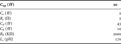
Figure 4 presents the physical structure of the switch from an electromagnetic perspective and its equivalent circuit model. The total series capacitance between the beam and the RF line is composed of a parasitic series capacitance C s and the up-state capacitance C up. C d is the capacitance between the actuated electrode and the RF line separated by the thin dielectric layer. C b is the parallel plate capacitance formed between the actuation electrode and the MEMS plate. Since R b is very large, the bias network has a negligible effect on the RF performance of the device. The element L s comes from the length of the input–output CPW line. R on represents the contact resistance. The different values of the lumped elements are given in Table 2.

Fig. 4. Lumped-element model of the RF MEMS contact.
Table 2. Lumped-element model parameters.
V. RF PERFORMANCE AND MEASUREMENT
A) Pull-down and release voltages
An automated test bench with Labview software has been used to measure the behavior of the electromechanical switch. The bench RF system determines the component state by modulating an RF signal by the height of the beam.
The pull-down and release voltages are detected by applying a triangular voltage bias signal. The beam position is known from measurement of the power level detected by a diode at the output of the RF-MEMS.
As it can be seen in Fig. 5, the RF-MEMS switch presents 6 V pull-down voltage and 3 V release voltage. Note that at 8 V, the beam collapses around the dimple.

Fig. 5. Pull-down V p and release voltage V r of the RF-MEMS switch experimental determination from P detected = f(V bias) curve.
B) S-parameters
All testing are done on a probe station in a standard laboratory environment without atmosphere or pressure control and with an SOLT calibration planes at AA' (see Fig. 2). Figure 6 presents measured and simulated S-parameters in up and down states position. It shows a high isolation of 30 dB at 2 GHz in the up state. The fitted off capacitance (composed from the C s in parallel with C up) C off is 22 fF in good agreement very well with Agilent-ADS simulations. When a 10 V bias voltage is applied, the insertion losses are 0.17–0.19 dB and return loss better than 33–35 dB at 2 GHz. The fitted contact resistance R on is <2 Ω (Au–Au contact). The insertion loss of 0.17–0.19 dB include both the resistance contact R on and loss of the whole circuit, it is demonstrated by measuring the S-parameters of a switch fabricated on the down state and as a result for that, it presents 0.1 dB of insertion loss. Then, the intrinsic R on contact resistance can be estimated at <1 Ω.

Fig. 6. Measured and simulated S-parameters (a) in down-state position at 10 V and (b) in up-state position.
The figure-of-merit for the RF-MEMS metal-contact switch can be expressed in two ways [Reference Stefanini, Chatras, Blondy and Rebeiz20]:
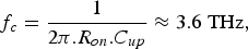 $$f_c=\displaystyle{1 \over {2\pi .R_{on} .C_{up} }} \approx 3.6\; {\rm THz\comma \; }$$
 $$R_{on} .C_{up} \approx 44\, {\rm fs}.$$
The two figures of merit of the resistive switch reflect the good RF performances of the device.
C) Switching time
One of the major advantages of scaling down MEMS cantilevers is significant reduction of effective mass resulting in an increase in the resonant frequency and a decrease in the switching time, even if the control voltage is low. Switching speed measurement has been done using the specific test bench shown in Fig. 7. In this setup, the MEMS component bias signal is generated by a frequency generator and amplified using a wide band high-voltage amplifier. The induced bridge motion over time can be detected by measuring the amount of RF signal reflected at the component input. This reflected signal is collected by a circulator, and then sent to a diode detector, and the bridge displacement can be detected using an oscilloscope. A wideband power meter with 8 ns resolution completes this test setup to accurately detect the beam switching delay compared to the actuation signal. MEMS structures have been tested under vacuum and actuated using a 10 kHz bipolar signal in order to limit dielectric charging issue and ensure time stable measurement. Switching speed measurement has been done for different actuation voltages. For an 8 V bias voltage, the switching time is 9 µs, and then as the applied voltage increases, the switching time decreases substantially to reach 4.5 µs at 11 V bias voltage as shown in Fig. 8.

Fig. 7. Switching speed measurement test bench.

Fig. 8. Switching time for different applied bias voltages.
The bouncing shown in Fig. 8 could be explained by the fact that the measurements are done in vacuum environment.
VI. RELIABILITY
The sensitivity of the device to dielectric charging has been tested using an automated test bench that records pull-in and pull-out voltages automatically. The MEMS device is left in the down state with 10 V (DC) applied and the pull-in and pull-out voltages are recorded every 3 s. The tests were conducted in vacuum and the results are plotted in Fig. 9.

Fig. 9. Evolution of V p over time.
It can be seen that the pull-in voltage has a very small evolution over time, from an initial value of 8.5 V, up to 9 V after 90 min. No specific optimization was done on the dielectric layer and the results are showing the small sensitivity of these devices to charge retention.
VII. CONCLUSIONS
This paper presents a new concept of metal-contact RF-MEMS switch using nanometer electrostatic gaps. The deposition of a dielectric layer allows achieving a relatively large electrostatic force in the down-state position for a given voltage. The pull-down voltage can be reduced substantially (below 10 V) by scaling down the gap and still ensuring a good contact force. The concept was validated by measuring the insertion loss on the down-state position which was below 0.2 dB at 2 GHz. The effective contact resistance is approximated to <2 Ω, resulting in a 44 fs figure-of-merit. Moreover, scaling down the gap permits reducing the pull-down voltage further and increase the stiffness of the device. It was demonstrated also that by having a low pull-down voltage, the charge retention issues are minimized, through pull-in voltage measurements.
Work is on-going in our laboratory for reliability testing and power-handling. In a long-term view, further miniaturization and integration into CMOS circuits will be conducted.
 Achref Yahiaoui received the Master's degree in circuits, systems, and micro and nanotechnology for optical and high-frequency communications from the University of Limoges, Limoges, France. He is currently toward the Ph.D. degree in high frequency communications in the XLIM laboratory, University of Limoges. He served a 6-month internship in the Electrical and Computer Engineering Department of the University of California at San Diego, La Jolla. His research interests include microelectromechanical systems devices.
 Emilien Lemoine received the Master's degree in Circuits, Systems, and Micro and Nanotechnology for optical and high frequencies telecommunications in 2011 from University of Limoges in France. He is currently toward the Ph.D. degree in reliability of RF MEMS in Xlim laboratory in the University of Limoges, Limoges, France.
 Arnaud Pothier received the Ph.D. degree in Electrical Engineering from the University of Limoges, Limoges, France, in 2003. He is currently a Full-Time Researcher with the Centre National de la Recherche Scientifique (CNRS), XLIM, University of Limoges. His current research activity is focused on the tunability functions development and implementation for analogical communication modules using RF MEMS components especially for reconfigurable/programmable filters and phase shifters.
 Pierre Blondy (M'99) received the Ph.D. and Habilitation degrees from the University of Limoges, Limoges, France, in 1998 and 2003, respectively. From 1998 to 2006, he was with the Centre Nationalde la Recherche Scientifique, as a Research Engineer with the Xlim Laboratory, where he began research on radio frequency microelectromechanical system (RF MEMS) technology and applications to microwave circuits. He is currently a Professor at the University of Limoges, leading a research group on RF MEMS and he is holding an Institut Universitaire de France chair, to conduct research on innovative microwave circuits. He was a Visiting Researcher at the University of Michigan, Ann Arbor, in 1997, and at the University of California at San Diego, La Jolla, in 2006 and 2008. He has authored or coauthored more than 150 papers in refereed journals and conferences proceedings. Dr. Blondy was an Associate Editor for the IEEE MICROWAVE AND WIRELESS COMPONENTS LETTERS in 2006. He has been a member of the IEEE International Microwave Conference Technical Program Committee since 2003. He was the recipient of the MTT-S “Outstanding Young Engineer Award” in 2011 for his research on RF MEMS.


