Introduction
In recent years, millimeter-wave (MMW) spectra (such as E-band, V-band, and Q-band) have been investigated for wireless backhauling application [Reference Dehos, González, De Domenico, Ktenas and Dussopt1, Reference Pi, Choi and Heath2]. These large continuous bandwidths provide a viable and cost-effective approach to data linkages between vast 5 G small cells and the core network. Waveguide power combiners are considered to boost the output power of MMW transmitters, to support their huge traffic load and atmospheric attenuation. The metal-pipe rectangular waveguide (MPRWG)-based power combiner [Reference Pi, Choi and Heath2–Reference Guo, Li, Huang, Shao, Ba, Xie, Jiang and Deng6] has lower loss than its planar transmission-line counterparts (such as the coplanar waveguide or microstrip). This merit makes MPRWG technology attractive for applications in which dissipative attenuation is critical. However, the manufacturing cost of such complex three-dimensional structures hinders their wider applications. This disadvantage is further exacerbated when the frequency moves upward to the MMW band. To overcome this constraint, several alternative manufacturing technologies for MMW MPRWG components [Reference Zhang and Zirath7–Reference Ermolov, Lamminen, Saarilahti, Wälchli, Kantanen and Pursula9] have been proposed, providing shorter lead-times, enhanced productivity, and reduced volume size. It is, however, essential that a cost-effective yet sufficiently accurate measurement technique is to be developed for low-cost, large-volume technology platforms to facilitate the widespread use of MMW MPRWG components.
The existing techniques for waveguide power combiner measurement fall into two main categories: hot tests (with driver unit amplifiers (UAs)) and cold tests. Hot tests require the coherent operation of numerous driver UAs, and thus are typically confined to final verification. Cold tests, conversely, provide economical alternatives for electrical performance monitoring and early fault detection. In term of hardware, a cold test is typically conducted by means of either a twin structure, comprising an interconnected, mirrored divider combiner, or a standalone combiner treated as a divider.
In the first cold test arrangement, although a back-to-back method is available for the two-port device under test (DUT) [Reference Martens10], there is currently no effective way to apply this method to multiport DUT cases. A slight variant of this method has been previously explored for the waveguide traveling-wave power combiner (TWPC) [Reference Li, Hilliard, Shafer, Daggett, Dickman and Becker11]; however, spikes on the frequency response proved to be problematic. Despite extra countermeasures to cope with the spikes, the application of this divide-by-two method to TWPC is confined to a limited frequency span.
In the second cold test arrangement, the non-coaxial interface of the combiner poses a critical obstacle to accurate scattering parameter measurement in terms of its densely populated parallel ports, the MMW operating frequency range and the resulting complexity of the test fixture. Due to the lack of a multiport counterpart for two-port thru-reflect-line calibration, the necessary de-embedding to move the reference planes of a vector network analyzer (VNA) to the intrinsic ports is difficult. To minimize the burden of test fixture fabrication and modeling, an indirect multiport method, referred to as the “port reduction method” (PRM), is revised here, which can be utilized effectively for the scattering parameter measurement of N-port MPRWG devices with a two-port VNA.
As delineated in Fig. 1, only the partial ports of the DUT are extended to VNA inputs through the test fixture, significantly reducing the fixture complexity. Additionally, all remaining DUT ports (usually ports that are difficult to access, or cannot be reached directly) are terminated using configurable auxiliary terminators. Moreover, a thorough examination of the multiport DUT can be achieved by using prearranged reflections of auxiliary terminators. As a result, the entire DUT scattering matrix can be obtained from the measurements acquired from the partial ports. This is known as the PRM method, and its working principle has already been deduced in [Reference Rolfes and Schiek12]. Therefore, considering the diverse configurable states of termination at an individual port, a set of well-chosen termination conditions should be established for measurement purposes. Multiple scanning measurements relying on these specified conditions provide sufficient intermediate data to reconstruct the entire scattering matrix of the DUT. Consequently, the obtained intermediate data (a set of low-dimensional matrix data) are utilized to reconstruct the DUT scattering matrix, which is an (N + 1) dimensional matrix, using a reconstruction algorithm. For instance, experimental verification has been previously reported on an X-band eight-way bus-bar divider/combiner [Reference Lonac, Melczarsky and Paganelli13], as well as on an HDMI digital bus [Reference Kam and Kim14]. In brief, the validity of the PRM method relies on two foundational aspects [Reference Chen and Chu15]: an accurate model of a custom-made auxiliary termination and the robustness of the reconstruction algorithm. However, the accuracy of reconstruction algorithm tends to be unstable and, therefore, the ultimate accuracy of the PRM method is limited [Reference Chen and Chu16]. This issue of accuracy may be monitored and remedied by exploiting the respective condition number associated with the crucial matrix inversion operations inside the algorithm. In practice, large condition numbers commonly lead to ill-conditioned numerical calculations. This is the reason that remedial works of error detection and recalculation are often researched. Specifically, with respect to MMW MPRWG component, the PRM method normally relies on an augmented second tier of VNA calibration by means of dedicated calibration kits ([Reference Jargon, Arz and Williams17, Reference Judaschke18]) to minimize the post-calibration residual errors, thereby ensuring accuracy. In summary, the two extant methods discussed above do not fully address the needs of TWPC characterization.

Fig. 1. Measurement setup for N-port non-coaxial device based on PRM method.
This paper proposes a cold test method, namely the “cushioned pair method”, which accommodates the design refinement of a TWPC. The cushioned pair method is not limited in terms of bandwidth and its formulation includes an alternative reconstruction algorithm which does not necessitate the unsettled matrix inversion. An in-situ implementation was conducted to validate the effectiveness of the proposed method under real-world requirements.
This paper is organized as follows: section “Problem description and working principle of cushioned pair method” describes the general problem of characterizing a multiway TWPC and presents the principle of the proposed method. Although the theoretical framework of our method bears resemblance to that of a previous work [Reference Gupta19], two crucial distinctions exist between the key formulas in this paper and that in the previous one. In brief, the improved expression has a wider applicable scope, making it better suited to the asymmetrical combiner exemplified by the TWPC. Moreover, a practical implementation of the cushioned pair method is quantitatively analyzed in section “Problem description and working principle of cushioned pair method”. Section “Fabrication and measurement” reports a representative example of a Q-band MPRWG-based TWPC and delineates each step of the proposed approach. Section “Conclusions” provides a brief summary and conclusion.
Problem description and working principle of cushioned pair method
Introduction to the waveguide traveling-wave power combiner
The TWPC is an asymmetric longitudinal one-dimensional spatial power combiner, which is flexible in its number of amplifier channels. A physical model of a combined amplifier module utilizing a TWPC is presented in Fig. 2. Its essential components are highlighted in Fig. 2(a) and its schematic is presented in Fig. 2(b). Entering from the left side, the input signal is coupled from the waveguide divider onto each microstrip, thereafter reaching each UA. After amplification, the signals from each UA are combined at the TWPC on the right side via a reverse process. The assembly of its E-plane split-block is shown in Figs 2(c) and 2(d). The bulky metal walls of the waveguides are merged with chip carriers for MMICs to provide electrical and thermal conductivity. A PCB incorporating the planar E-plane probes is mounted above the metal base. A key indicator representing the compactness of the combiner is the interval distance L UX (Fig. 2(a)). Its typical value is approximately 1/8 λ G, which is equal to 1.53 mm at a frequency of 36 GHz.

Fig. 2. Physical model of a combined amplifier module utilizing TWPC. (a) Essential components of a combined amplifier based on TWPC; (b) schematic diagram of the combined amplifier; (c) overall view of a representative combined amplifier module realized by E-plane split-block assembly; (d) bottom half of E-plane split-blocks.
One of the advantages of the combiner, in addition to its low volume and weight, is that its compactness reduces the insertion loss. However, such compactness also gives rise to challenges in its testability. A compact combined amplifier module lacks sufficient space for a test fixture containing a parallel row of end-launch coaxial connectors in parallel [20]. An enlarged variant of the prototype in Fig. 2 can be built separately for measurement purposes, but in-situ measurement carried out on the prototype itself is more advantageous, due to its rapid operation and the elimination of the repeatability concern related to second sample fabrication. Rotational symmetry between the divider and combiner, illustrated in Fig. 2, was therefore utilized in this study to suit the proposed method.
Working principal of the cushioned pair method
In this study, an RF system in which multiple coherent sources collectively drive a single load through a passive (N + 1) port power-combining network, as shown in Fig. 3, was investigated. The input ports of the network are labeled sequentially while the output port is labeled “o”. The network is represented by an (N + 1) dimensional S-matrix S C, and a crucial vector (CV)  ${\mathop{\zeta} ^{\hskip-4.4pt\vskip-2.5pt \rightharpoonup}}$ within S C is defined in equation (1) to facilitate subsequent deductions. The coherent sources are represented by an excitation signal vector (ESV)
  ${\mathop{b^G}\limits^{\rightharpoonup}}$, the components of which are denoted as
  $b_k^G $. Here, the power-combining efficiency of the power combiner termed as η C is expressed in terms of
  ${\mathop{\zeta} ^{\hskip-4.4pt\vskip-2.5pt \rightharpoonup}}$ and
  ${\mathop{b^G}^{\hskip-7pt\vskip-2.4pt\rightharpoonup}} $ in equation (2).
 $$S^C = \left[ {\matrix{ {\matrix{ {s_{11}} & {s_{12}} & \cdots & {s_{1N}} \cr {s_{21}} & {s_{22}} & \cdots & {s_{2N}} \cr \vdots & \vdots & \ddots & \vdots \cr {s_{N1}} & {s_{N2}} & \cdots & {s_{NN}} \cr}} & {\matrix{ {s_{1o}} \cr {s_{1o}} \cr \vdots \cr {s_{No}} \cr}} \cr {\underbrace{{\fbox{{\matrix{ {\hskip1pts_{o1}} & {\hskip1pts_{o2}} & \hskip2pt\ldots & { s_{oN}} \cr}}}}}_{\mathop{\zeta}\limits^{\rightharpoonup}} {\hskip9pt s_{oo}\hskip-23pt}}}} \right],$$
 $$\eta _{C} = \left.{\displaystyle \big \vert { {\sum s_{ok} \cdot {b_k^G}} \big \vert}^2 \over \sum {{ {\big \vert} {b_k^G}} {\big \vert}}^2} \right\vert _{k\, = \, 1,2,\cdots, N} = \displaystyle{1 \over {\left \Vert {\mathop {b^G}\limits^{\rightharpoonup}} \right \Vert _2^2}} \bigg \langle {\mathop {\zeta}\limits^{\rightharpoonup}} \cdot {\mathop {b^G}\limits^{\rightharpoonup}} \bigg \rangle.$$
Fig. 3. Representation of general N-way power-combining circuit.
As per equation (2), combining efficiency η C depends not only on the intrinsic property of the combiner (CV  ${\mathop{\zeta}^{\hskip-4.4pt\vskip-2pt \rightharpoonup}} $), but also on the input signal (ESV
  ${\mathop{b^G} ^{\hskip-7pt\vskip-2.4pt\rightharpoonup}} $). According to the inner product computation in equation (2), the negative impact of numerical error propagation – as is manifested in the outcome of the accumulated error of η C – increases along with the path amount N. Equation (2) can be rewritten to alleviate this by defining two sets of variables: magnitude variable
  ${\kappa_{k_s}}$ and phase variable
  ${\rho_{k_s}}$ as in equations (4a) and (4b), respectively.
 $$\eta _C = \left \vert \sum \big \vert {b_k^G} \big \vert ^2 \kappa_k \cdot \exp \,(\,j\rho_j) \right \vert^2\cdot \left \Vert {\mathop{\zeta}\limits^{\rightharpoonup}} \right \Vert _2^2, $$
 $$\kappa _k = \left(\displaystyle {\Big\vert s_{ok} \Big\vert \over \Big\Vert {\mathop{\zeta}\limits^{\rightharpoonup}} \Big\Vert_2 }\right){\bigg /} \left( {\displaystyle \Big\vert b_k^G \Big\vert \over \Big\Vert {\mathop{b^G}\limits^{\rightharpoonup}} \Big\Vert_2 }\right),$$
 $$\rho_k = Arg\lpar {b_k^G \cdot s_{ok}} \rpar.$$
Next, the effect of κ ks and ρ ks within equation (3) can be represented by three statistical parameters of κ ks and ρ ks, namely M T, M V, and δ RMS, as defined over κ ks and ρ ks in equations (5a)–(5c); respectively. As a result, equation (3) is further reformulated as equations (6a)–(6d), thereby establishing a confidence interval estimation of η C that supersedes the previous single point estimation. The individual contribution of each statistical parameter is also explicitly distinguishable. Specifically, the lower bound of η C interval estimation, termed as Η, is decomposed into three constituent factors: HM, HP, and HD in equation (6a). These factors are provided individually. HM, which represents the effect related to κ ks, is mapped to a function of M T and M V. Similarly, HP, which represents the effect related to ρ ks, is mapped to a function of δ RMS, while HD represents the other effect of dissipative loss. By way of further clarification, stddev in equation (5c) represents the standard deviation function and Geomean in (6c) represents the geometric mean function. A proof of equations (6a)–(6d), based on general inequality theorems [Reference Drachman and Cloud21–Reference Mitrinovic, Pecaric and Fink24], is provided in the appendix.
 $$M_T = {\rm Max}\lpar {\kappa_1,\kappa_2,\cdots, \kappa_n} \rpar,$$
 $$M_V = {1 / {\min \lpar {\kappa_1,\kappa_2,\cdots, \kappa_n} \rpar }},$$
 $$\delta _{RMS} = stddev\lpar {\rho_1,\rho_2,\cdots, \rho_n} \rpar,$$
 $$\eta _c \ge H{\rm}={\rm } H^M\cdot H^P\cdot H^D,$$
 $$H^M = \displaystyle{{4M_VM_T} \over {{\lpar {1 + M_VM_T} \rpar }^2}},$$
 $$\eqalign{&\displaylines{H^P\approx \lsqb {Geomean\lpar {\cos \lpar {\rho_1} \rpar,\cdots, \cos \lpar {\rho_n} \rpar } \rpar } \rsqb ^2, }\cr& \quad\approx \cos ^2\lpar {\delta_{RMS}} \rpar } $$
 $$H^D = \left \Vert {\mathop{\zeta}\limits^{\rightharpoonup}} \right \Vert _2^2.$$
With respect to the practical application of the formulation in equations (6a)–(6d), HD is usually determined once by the implementation process, in relation to the material properties or combiner architecture. HD is therefore not considered during the design refinement process. HM and HP are closely related to the experimental design optimization of the combiner performance. In typical cases, HP outweighs HM as the dominant factor in η C degradation.
To provide an intuitive understanding of equation (6), η C dependence with respect to M T and δ RMS is illustrated in Fig. 4. The dependence of M V is omitted due to the symmetrical form of equation (6b). Three contour lines (0.975–0.925) mark the most commonly used zone while the color maps represent the gradient vector. The 0.975 contour line, as an example, intersects the axes at M T of 1.3 dB and δ RMS of 9°.

Fig. 4. Power-combining efficiency η C contour plots associated with M T and δ RMS.
The data collection process of κ ks and ρ ks is discussed in the next section.
In-situ implementation and associated methodical errors
The above methodology as it applies to a general power combiner was implemented in a TWPC (Fig. 2) by means of a set of test circuits. A flowchart of the three-step measurement procedure is shown in Fig. 5. The first measurement on circuit-A (Fig. 6(a)) was utilized to assess the overall performance of the power combiner. In the event of a defect within the combiner, although a declined overall performance can be observed, the position of the defect must also be located. As supplementary means, the latter two measurements on circuit-B and circuit-C (Figs 6(b) and 6(c), respectively) may be used successively to determine the position and severity of the defect.

Fig. 5. Flowchart of TWPC measurement during the design cycle.

Fig. 6. Schematic diagram of TWPC test circuits. (a) Schematic diagram of test circuit for η C measurement marked as circuit A; (b) schematic diagram of test circuits for measurement of ρ ks marked as circuit B; (c) schematic diagram of test circuits for measurement of κks marked as circuit C.
Considering the resemblance between Figs 6 and 2(b), an in-situ realization of the test circuit (Fig. 6) was achieved by adopting miniature components. In this case, the space reserved for UAs (Fig. 2(d)) was reused. First, the reserved space could accommodate pairs of attenuator chips (Figs 6(a) and 6(b)). Second, the schematic in Fig. 6(c) can be realized in a similar way – although the original PCB (Fig. 2(d)) should be replaced by a subtly modified PCB to draw out the output voltages of the power detectors. The primary advantage of the in-situ implementation is that the planar transmission-line interface of the combiner is directly used, thereby avoiding a coaxial-to-non-coaxial fixture. This in-situ implementation also basically eliminates any methodical errors due to the inherently poor return loss of the TWPC input ports. A quantitative analysis of the methodical errors associated with this in-situ implementation is provided below for comparison against other methods.
First, a calculation equation of η C was derived based on the cushioned pair structure in Fig. 6(a). Accordingly, the η C outcome was determined by the composite transmission coefficient of the entire structure. The methodical error associated with the equation, termed as ɛη, is also provided here. Let α L and α R denote the attenuation value of the attenuator array on the left and right, respectively, and let SD and SC denote the scattering matrices of the power divider and combiner (Fig. 6(a)), respectively. To facilitate subsequent formulations, SD and SC are partitioned into block matrices in the form of equations (7a) and (7b), where S BB and S CC are matrices of order n × n, and S AB and S CD are matrices of order 1 × n and n × 1, respectively. Diagonal matrices Λ L and Λ R are defined in equations (7c) and (7d) to represent the transmission response of the attenuators, wherein db2mag denotes the decibel to linear magnitude conversion function.
Based on the above terms, the transmission coefficient of the entire structure in Fig. 6(a) (termed as TG) is derived in equation (8) by means of the multiport network theory [Reference Mongia, Bahl and Bhartia25]. For ease of comparison, η C is also expressed by S AB and S CD in equation (9). The comparison indicates that the middle term on the right side of equation (8), which is denoted as f(α L, αR), impedes the calculation of η C from TG. In essence, the f(α L, αR) function explicitly represents the damped multiple reflections within the structure.
 $$S^D = \left[ {\matrix{ {\matrix{ {S_{AA}} & {} \cr {} & {} \cr}} & {\matrix{ {S_{AB}} \cr {} \cr}} \cr {\matrix{ {S_{BA}} & {} \cr}} & {S_{BB}} \cr}} \right],$$
 $$S^C = \left[ {\matrix{ {\matrix{ {S_{CC}} & {} \cr {} & {} \cr}} & {\matrix{ {S_{CD}} \cr {} \cr}} \cr {\matrix{ {S_{DC}} & {} \cr}} & {S_{DD}} \cr}} \right],$$
 $$\Lambda _L = {\rm db2mag}\,{\rm (}-\alpha _L{\rm )}\cdot U,$$
 $$\Lambda _R = {\rm db2mag}\,{\rm (}-\alpha _R{\rm )}\cdot U,$$
 $$T^{_G} = S_{AB}\Lambda _L\lsqb {U-\lpar {\Lambda_LS_{BB}\Lambda_L} \rpar \lpar {\Lambda_R\cdot S_{CC}\Lambda_R} \rpar } \rsqb ^{-1}\Lambda _RS_{CD},$$
 $$\eta _{\rm C}{\rm}={\rm } \displaystyle{{S_{AB}S_{CD}} \over {S_{AB}S_{AB}^T}}. $$
To address this issue, f(α L, αR) is first expanded into a Taylor series and, subsequently, matrix Taylor series truncation [Reference Higha26] is used to simplify the formula. The relation between η C and TG is thus established by linear approximation. The Taylor series expansion of f(α L, αR) presented in equation (10a) is established only under its convergence condition, which is also provided alongside in equation (10b). The consequent calculation equation is shown in equation (11). The associated methodical error ɛη produced by the series truncation can also be estimated by means of the corresponding matrix spectral radius in equation (10b). For instance, when α L and α R are set to 6 dB, the produced ɛη is around 3.1%. In view of such a minor ɛη, the calculation of η C from TG may be considered to satisfy common requirements.
 $$\eqalign{\,f\lpar {\alpha_L,\alpha_R} \rpar &= [U-\lpar {\Lambda_LS_{BB}\Lambda_L} \rpar \lpar \Lambda_RS_{CC}\Lambda_R \rpar ]^{-1} \cr & = U + \sum\nolimits_1^{\infty} \lpar \Lambda_LS_{BB}\Lambda_L \cdot \Lambda_R S_{CC} \Lambda_R \rpar^k \cr & \approx U,}$$
 $$\eqalign{\left \Vert \Lambda_L S_{BB}\Lambda_L \cdot \Lambda_R S_{CC} \Lambda_R \right \Vert_2 \le \left \Vert \Lambda _L \right \Vert_2^2 \left \Vert \Lambda _R \right \Vert _2^2 \left \Vert S_{BB} \right \Vert_2\left \Vert S_{CC} \right \Vert_2 \cr \le {\rm db2mag} \lpar {-\alpha_L-\alpha_R} \rpar,} $$
 $$\eta _C = {\rm db2mag}\left[ {\displaystyle{{\lpar {\alpha_L + \alpha_R} \rpar } \over 2}} \right]\cdot \sqrt {\vert {T^G} \vert }. $$
Similarly, the methodical error related to ρ ks, referred to as ɛρ, can also be assessed by a Taylor series expansion. When α L and α R (Fig. 6(b)) are 6 dB, the resultant error ɛρ is around 1.8°.
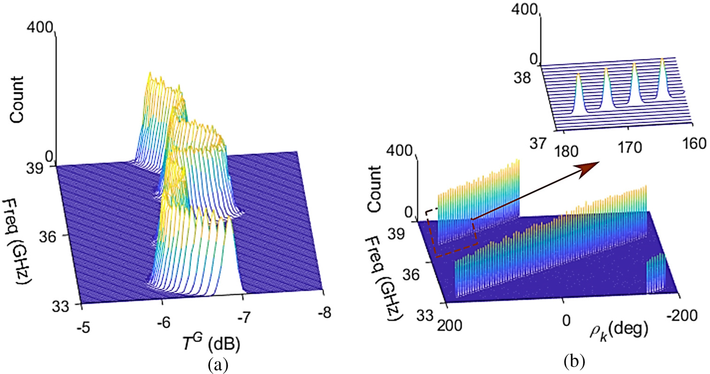
A quantitative analysis was also conducted in this study by means of Monte Carlo (MC) simulation with respect to the negative impact of attenuator variation. Considering the standard deviation values of δ(T G) and δ(ρ k) shown in Figs 7(a) and 7(b), respectively, the typical values are unveiled as δ(T G) <0.088 dB and δ(ρ k) <0.19°, on the condition that regular chip attenuators are employed. These modest values suggest that the impact of attenuator variation is estimable and treatable.

Fig. 7. Histograms of typical MC simulation results (1500 trials). (a) TG fluctuation owing to attenuator variation; (b) ρk fluctuation owing to attenuator variation.
The methodical error of κ ks (termed as ɛκ) is determined from the expression of κ ks in equation (12), wherein γ V is the voltage sensitivity of the power detectors, while  $v_k^L $ and
  $v_k^R $ are output voltages of the power detectors in Fig. 6(c).
 $$\kappa _k = \left( {\displaystyle{1 \over {\gamma_V}}} \right)\cdot \left( {\displaystyle{{v_k^R} \over {v_k^L}}} \right)$$
 The main error source of ɛκ is ascribed to γ V, whereas the contributions of  $v_k^L $ and
  $v_k^R $ are negligible. To enhance the accuracy of γ V, the response of a power detector is usually calibrated by a power meter. Therefore, the error of γ V depends on individual variations in a set of power detector, as well as the error of the power meter. In a typical case at the MMW band, the variation [27] contributes 0.10–0.20 dB, while the power meter error [28] contributes 0.13–0.17 dB to ɛκ. Thus, a typical ɛκ ranges from 0.23 to 0.37 dB.
The typical values of the three error terms discussed above are listed in Table 1. The proposed method provides sufficient precision for regular applications. The specific requirements of auxiliary hardware can also be determined according to the targeted measurement deviations.

Fabrication and measurement
A Q-band four-way waveguide TWPC with a 33–39 GHz operational frequency was evaluated by means of the proposed method. Photographs of the entire prototype module, as well as microphotographs of the chip mounting, are provided in Fig. 8. Split-block geometries of the waveguide combiner and UAs are shown in Figs 8(a) and 8(b). Microphotographs of the amplifier MMIC mounting and chip attenuator mounting are shown in Figs 8(c) and 8(d), respectively.

Fig. 8. Photograph of the fabricated prototype. (a) Photograph of entire combined amplifier module; (b) photograph of bottom half of E-plane split-blocks; (c) microphotograph of amplifier MMIC mounting; (d) microphotograph of chip attenuator mounting.
The mechanical part of the waveguide TWPC was fabricated on a 6061 aluminum alloy plate by a computer numerical control machining. A conventional carbide drill was used for the cut. The positional accuracy of the device is 20 µ and the roughness R a (arithmetic mean surface roughness) is within a range of between 0.8 and 1.6 µ. The E-probe array and microstrip were realized on 0.254 mm-thick TLY-5 substrate (Taconic) with 17 µm electrodeposited copper cladding.
The in-situ implementation of the test circuits (Figs 6(a) and 6(b)) is shown as a close-up photograph in Fig. 8(d) in the context of Fig. 8(b). A thin film attenuator ATN3580 series (Skyworks) [29] was used in the test circuits. To facilitate the measurements, 6 dB attenuators were used consistently for the through path, while 12 dB attenuators of equal footprint were used for load termination (Fig. 6(b)). Switching from the test circuits shown in Fig. 6(a) to those shown in Fig. 6(b) was achieved simply by replacing the passive chips. The dimensions of the PCB apertures for MMIC are 2.15 × 1.80 mm, and the footprint of the attenuator is 0.69 × 0.74 mm. The measurements were accomplished by means of a two-port VNA with a pair of WR-22 waveguide-to-coax adapters.
Figure 9 shows both the simulated and measured data of the transmission coefficient TG and their derived values of power-combing efficiency η C. The simulated data were obtained by co-simulation with Ansys HFSS and Keysight ADS. The gap between the simulated and measured results reflects mainly the extra conductive loss owing to the random rough metal surface. The measured power-combining efficiency η C is close to 90%, with the exception of a slight dip at the low end of the frequency span. Based on an empirical estimation, the measured η C of the prototype is consistent with the expected value derived from the process capabilities of the constituent parts: the MPRWG component by an E-plane split-block process [Reference Stil, Fontana, Lefranc, Navarrini, Serres and Schuster30, Reference D'Auria, Otter, Hazell, Gillatt, Long-Collins, Ridler and Lucyszyn31] and a planar E-plane probe [Reference Samoska32]. Furthermore, the η C performance of this prototype is relatively close to that of a counterpart with a more sophisticated process [Reference Chu, Kang, Wu and Mo33].

Fig. 9. Simulated and measured transmission coefficient TG and corresponding η C values.
Figure 10(a) shows the simulated and measured phase shift ρ ks of the individual branches. Figure 10(b) provides the δ RMS and HP values obtained from measured ρ ks. In view of the consistent curves in Figs 8 and 10(b), the frequency responses of η C and HP are in sufficiently close agreement. Taken together, these data may provide a workable reference for the further TWPC design refinement. For instance, according to the value of ρ ks, suitable phase trimmers [Reference Li, Hilliard, Shafer, Daggett, Dickman and Becker11] can be attached to the input interface of the TWPC.

Fig. 10. Simulated and measured data of ρ ks along with measured δ RMS and HP. (a). Frequency response of simulated and measured ρ ks. (b). Frequency response of measured δ RMS and HP.
The κ ks measurement depicted in Fig. 6(c) remains unfinished due to a shortage of power detector chips. Although the data of κ ks and their corresponding HM values are absent, the proposed method is still delineated by this example because the contribution of HM is independent and subordinate to HP, as indicated by the contour plot in Fig. 4. In addition, the contribution of HM in this example is minor owing to the attractive coupling mechanism of the E-plane waveguide probe (which has been evaluated empirically in [Reference Eshrah, Kishk, Yakovlev and Glisson34]). Assuming that the waveguide TWPC is realized in an alternative form of longitudinal slots [Reference Jiang, Ortiz and Mortazawi35, Reference Pérez, Kosmopoulos and Goussetis36], a less agreeable κ k characteristic should emerge due to its more complex coupling mechanism, thus enlarging HM.
Table 2 shows a comparison of the cushioned pair method against other state-of-the-art methods at the MMW band. The most notable advantages of the proposed method include quicker hardware fabrication and simpler post processing of the acquired data.
Table 2. Comparison with previous methods

Conclusions
This paper presents the cushioned pair method for MMW TWPC characterization up to the intrinsic ports. The primary advantage of this method is that all measurements are performed in-situ, thereby precisely revealing all impacting factors in real time. The prototype fabrication and measurement processes under the proposed method can also be accelerated by supplementary commercial off-the-shelf components, thereby precluding the time-consuming work of fabricating and modeling customized terminators.
Acknowledgement
This work was supported by the National Natural Science Foundation of China under Grant 61671149.
 Honglei Sun received his B.S. degree in Electronic Engineering in 2004 from Tianjin University, Tianjin, China. He is currently working toward his Ph.D. at the State Key Laboratory of Millimeter Waves, Southeast University, Nanjing, China. His research interests include RF/microwave/millimeter-wave power amplifiers (PA) and linearized transmitters for wireless communication. From 2005 to 2008, he held a Development Engineer position with Huawei Technology, where he was involved in the design of PAs for the GSM macro base-station. From 2011 to 2013, he was employed as a radio design engineer with Ericsson China, where he was involved in several power amplifier projects for WCDMA and LTE base-station.
 Xiao-Wei Zhu (S'88-M'95) received his M.E. and Ph.D. degrees in Radio engineering from Southeast University, Nanjing, China in 1996 and 2000, respectively. He has been with Southeast University since 1984, where he is currently a professor at the School of Information Science and Engineering. Dr. Zhu has authored and co-authored more than 90 technical publications, and holds 15 patents. His research interests include RF and antenna technologies for wireless communications, microwave and millimeter-wave theories and technologies, as well as power amplifier (PA) non-linear character and its linearization research with a particular emphasis on wideband and high-efficiency GaN PAs. Dr. Zhu is the President of the Microwave Integrated Circuits and Mobile Communication Sub-Society, the Microwave Society of CIE, and Secretary of the IEEE MTT-S/AP-S/EMC-S Joint Nanjing Chapter.
 Xuesong Shi was born in Xi'an, Shaanxi Province, China, in 1993. He received the B.S. degree in Communication Engineering from Southeast University in 2016 and he is currently working toward his M.S. degree at the State Key Laboratory of Millimeter Waves, Southeast University, Nanjing, China. His specific focus is electromagnetic field and microwave technology, and his study direction includes RF/microwave passive circuits such as filters, couplers, and mixers.
 Ruijia Liu was born in Nanjing, Jiangsu Province, China, in 1995. He received his B.S. degree in Electronic Information Science and Technology from Southwest Jiaotong University, Chengdu, China, in 2017. He is currently working toward his Ph.D. degree at the State Key Laboratory of Millimeter Waves, Southeast University, Nanjing, China. His research interests include wideband microwave PA design and wideband millimeter-wave PA MMIC design.
Appendix
The lower bound of η C is established through its decomposition into a product of two factors: η a related to ρ ks and η b related to κks. With respect to η a, the superimposed effects of ρ ks rely solely on  $\lpar {\rho_k-\bar{\rho}} \rpar $, the relative deviation from their mean value, which is termed as δ k in equation (A2). Thereupon, the η C expression in equation (A1) is decomposed into separated expressions of η a and η b, given in equations (A3) and (A4).
 $$\eta _C = \eta _a\cdot \eta _b = \left \vert \sum \big\vert b_k^G \big\vert ^2 \kappa_k \cdot \exp \lpar {\,j\rho_j} \rpar \right \vert ^2\cdot \left \Vert {\mathop{\zeta}\limits^{\rightharpoonup}} \right \Vert _2^2, $$
 $$\delta _k = \rho _k-\bar{\rho}, $$
 $$\eqalign{\eta _a &= \displaystyle{{{\left \vert {\sum {\big \vert {b_k^G s_{ok}} \big \vert \exp \lpar {\,j\rho_k} \rpar }} \right \vert} ^2} \over {{\left( {\sum {\big \vert {b_k^G s_{ok}} \big \vert }} \right)}^2}} \cr &= \displaystyle{{{\left \vert {\sum {\big \vert {b_k^G s_{ok}} \big \vert \exp \lpar {\,j\delta_k} \rpar }} \right \vert} ^2} \over {{\left( {\sum {\big \vert {b_k^G s_{ok}} \big \vert }} \right)}^2}},} $$
 $$\eta _b = \displaystyle{{{\left( {\sum {\big \vert {b_k^G s_{ok}} \big \vert }} \right)}^2} \over {\sum {\vert {b_k^G} \vert }}}. $$
η a can be bound as follows: since the magnitude of a complex number is no less than its real part, η a in equation (A3) is estimated by equation (A5). Subsequently, the weighted arithmetic mean-geometric mean (weighted AM-GM) inequality theorem [Reference Drachman and Cloud21] is applied to equation (A5), thereupon inducing equation (A6). The superscripts in equation (A6), namely the weight factors, are already normalized and their sum is 1.
 $$\eta _a \ge \displaystyle{{{\left \vert {\sum {\big\vert {b_k^G s_{ok}} \big\vert \cos \lpar {\delta_k} \rpar }} \right \vert} ^2} \over {{\left( {\sum {\big \vert {b_k^G s_{ok}} \big \vert }} \right)}^2}},$$
 $$\eta _a \ge \left[ \prod \cos \lpar {\delta_k} \rpar ^{\big \vert b_k^G s_{ok} \big \vert \big / \big \Vert b_k^G s_{ok} \big \Vert_1} \right] ^2.$$
In practical cases, the values of these weight factors are close to each other because power combiners are usually designated for identical driving amplifiers. For this reason, these weight factors may be approximated as 1/N, leading to the geometric mean function in equation (A7). In this case, the contributions of κ ks to η a are completely omitted.
 $$\displaylines{\eta _a \ge \left[ {\prod {\cos {\lpar {\delta_k} \rpar }^{{1 / N}}}} \right]^2 \cr = \left [{Geomean\lpar {\cos \lpar {\delta_1} \rpar, \cos \lpar {\delta_2} \rpar, \cdots} \rpar }\right]^2.} $$
Intuitively, a root mean square (RMS) function is somewhat similar to a geometrical mean function; the RMS mean is usually preferable. An RMS alternative of equation (A7), which is expressed in equation (A8), is developed to enable a quicker calculation.
 $$\eqalign{&\displaylines{\eta _a \ge \left[ {Geomean\lpar {\cos \lpar {\delta_1} \rpar, \cos \lpar {\delta_2} \rpar, \cdots} \rpar } \right] ^2 }\cr& \quad \approx \left[ {\cos \lpar {\sigma_{RMS}} \rpar } \right]^2.} $$
 Additionally, the approximate equality between (A7) and (A8) can be proved by the Taylor's theorem in multiple variables [Reference Moskowitz and Paliogiannis22]. Let  ${\mathop{\delta}\limits^{\rightharpoonup}} = \left( {\matrix{ {\sigma_1,} \quad {\cdots,} \quad {\sigma_N} \cr}} \right)$ and consider two functions,
  $g\lpar {\vskip4pt \mathop{\vskip-3pt\delta}\limits^{\rightharpoonup}} \rpar $ and
  $\lpar {\vskip4pt\mathop{\vskip-3pt \delta}\limits^{\rightharpoonup}} \rpar $, as expressed in equations (A9) and (A10). In the ball zone around
  ${\mathop{z_r}\limits^{\rightharpoonup}} = \left( {\matrix{ {0,} \quad {\cdots,} \quad 0 \cr}} \right)$, a comparison between
  $g\lpar {\vskip4pt \mathop{\vskip-3pt \delta}\limits^{\rightharpoonup}} \rpar $ and
  $f\lpar {\vskip4pt \mathop{\vskip-3pt \delta}\limits^{\rightharpoonup}} \rpar $ can be carried out based on the first-order multivariable Taylor series expansion. The approximate equality can then be identified through the cross-examination of
  $g\lpar {\mathop{z_r}\limits^{\rightharpoonup}} \rpar $ and
  $f\lpar {\mathop{z_r}\limits^{\rightharpoonup}} \rpar $ in equation (A12) and that of the derivatives in equations (A13) and (A14).
 $$g\lpar {\vskip4pt \mathop{\vskip-3pt \delta}\limits^{\rightharpoonup}} \rpar = \prod {\cos {\lpar {\delta_k} \rpar }^{{1 / N}}}, $$
 $$f\lpar {\vskip4pt \mathop{\vskip-3pt \delta}\limits^{\rightharpoonup}} \rpar = \cos \left[ {{\left( {\displaystyle{1 \over N}\cdot \sum {\delta_k^2}} \right)}^{{1 / 2}}} \right],$$
 $$f\lpar {\vskip4pt \mathop{\vskip-3pt\delta}\limits^{\rightharpoonup}} \rpar = f\lpar {\vskip4pt\mathop{\vskip-3pt z_r}\limits^{\rightharpoonup}} \rpar + \nabla f\lpar {\vskip4pt \mathop{\vskip-3pt \delta}\limits^{\rightharpoonup}} \rpar \cdot \lpar {\vskip4pt\mathop{\vskip-3pt\delta}\limits^{\rightharpoonup}} -{\vskip4pt\mathop{\vskip-5pt z_r}\limits^{\rightharpoonup}} \rpar,$$
 $$f\lpar {\vskip4pt \mathop{\vskip-2pt z_r}\limits^{\rightharpoonup}} \rpar = g\lpar {\vskip4pt \mathop{\vskip-2pt z_r}\limits^{\rightharpoonup}} \rpar = 1,$$
 $$\displaystyle{{\partial g} \over {\partial \delta _k}} = \left( {-\displaystyle{1 \over N}} \right)\cdot g\lpar {\vskip4pt\mathop{\vskip-3pt\delta}\limits^{\rightharpoonup}} \rpar \cdot \tan \lpar {\delta_k} \rpar,$$
 $$\displaystyle{{\partial f} \over {\partial \delta _k}} = \left( {-\displaystyle{1 \over N}} \right)\left[ {\displaystyle{{\sin \lpar {\delta_{RMS}} \rpar } \over {\delta_{RMS}}}} \right]\cdot \delta _k.$$
Next, a lower bound for η b can be generated as follows: initially, the κ k range defined in equations (5a) and (5b) is restated into a single in equation (A12). Subsequently, equation (A12) is utilized to deduce equation (A13), which meets a weak precondition for the certain inequalities theorem complementary to Cauchy's inequality [Reference Diaz and Metcalf23, Reference Mitrinovic, Pecaric and Fink24].
 $$\displaystyle{1 \over {M_V}} \le \kappa _k \le M_T,$$
 $$\eqalign{& \big \vert {b_k^G} \big \vert ^2 \left( {\kappa_k- \displaystyle{1 \over {M_V}}} \right) \lpar{M_T-\kappa_k}\rpar \left(\big \Vert \zeta \big \Vert _2^2 / {\big \Vert {b^G} \big \Vert}_{2}^{2} \right) \cr & = \left( {\big \vert {s_{ok}} \big \vert - {1 \over {M_V}}\big \vert {b_k^G} \big \vert } \right) \bigg({M_T\big \vert {b_k^G} \big \vert - \big \vert {s_{ok}} \big \vert } \bigg ) \cr & \ge 0.}$$
Equation (A14) is then derived from equation (A13).
 $$\displaystyle{{{\left( {\sum {\big \vert {b_k^G s_{ok}} \big \vert }} \right)}^2} \over {\sum {{\big \vert {b_k^G} \big \vert } ^2\cdot \sum {{\big \vert {s_{ok}} \big \vert } ^2}}}} \ge \displaystyle{{4M_TM_V} \over {{\lpar {1 + M_TM_V} \rpar }^2}}.$$
By combining equations (A14) and (A3), a lower bound for η b can be derived in equation (A15).
 $$\eta _b \ge \displaystyle{{4M_TM_V} \over {{\lpar {1 + M_TM_V} \rpar }^2}} \big \vert \zeta \big \vert _2^2. $$
In summary, substitution of equations (A8) and (A15) into equation (A1) yields the lower bound of the combining efficiency η C in equations (6a)–(6d).