Introduction
Numerous wireless systems operate at several different frequency bands. For example, satellite system and modern GNSS systems employ signals at several frequency bands. For these systems, it is possible to utilize a few single-band circularly polarized antennas, with one antenna covering each frequency band independently. This, in any case, will prompt a large size, weight, and high cost of antenna and wireless systems. It is much more attractive if a single multi-band CP antenna can be employed for these applications, as it can result in a significant reduction in size, weight, cost, and complexity of wireless systems. The basic benefits of circular polarization are its high penetration capability compared with linear polarization and its ability of creating a reliable signal link irrespective of the antenna orientation of the device. The CP wave acquires two degenerated orthogonal modes with different resonant frequencies and there is a phase difference of 90° between two orthogonal modes.
Multi-band antenna with circular polarization plays an important role in wireless and satellite communication area because they can be used to reduce the loss of polarization mismatch and cover operation frequencies of various wireless communication systems. Thus, multi-band CP antennas have become a hot research topic in recent decades and a variety of techniques have been developed. There are different techniques for designing multi-band CP antennas, including multi-band CP microstrip patch antennas, multi-band CP slot antennas, multi-band CP DRAs, multi-band CP loop antenna [Reference Narbudowicz, Bao and Ammann1–Reference Hirose, Omori and Nakano8], and so on. Multi-band CP antennas can be obtained by utilizing the stacked patch arrangement. Multi-band CP antennas can be realized by using single-feed or multi-feed patches. The use of multi-feed patches can suppress undesired higher order modes and has higher polarization purity and broad bandwidth. But due to the expense of complicated feed network and a large feed size, single-feed design has advantages of a simple feed structure, compact size, and low fabrication cost. Single-feed slot-loaded patches and the dual-loop antenna are attractive for dual-band CP operations due to their advantages of a simple structure and easy fabrication.
There were several methods available in open literature to achieve broadband, dual-band, and multi-band operation for microstrip antennas [Reference Kanaujia and Vishvakarma9–Reference Kunwar, Gautam and Kanaujia16], because of their low profile with simple structure. Moreover, by specially designing of a microstrip line-fed wide-slot antenna, they can produce multiple operating frequency bands and CP radiation. Several technologies have been proposed to produce circular polarization [Reference Kumar, Gautam and Kanaujia17–Reference Sze and Pan22], all these designs only realize CP radiation at a single frequency. However, relatively few designs of dual-frequency slot antenna with dual orthogonal circular polarization have been reported in [Reference Rui, Li and Wei23–Reference Gautam and Kanaujia25]. In [Reference Khandelwal, Kanaujia, Dwari, Kumar and Gautam26], asymmetric slits loaded irregular-shaped microstrip patch antenna with good triple-band CP radiation characteristics. Further antennas with various shapes of microstrip feed line and rectangular wide slot have been introduced for triple impedance bandwidths with CP radiations [Reference Wang, Guo and Sheng27–Reference Bao and Ammann31]. A single-feed tri-band CP annular slot antenna is designed to operate at the L1 and L2 bands that are presented in [Reference Wang, Guo and Sheng27]. Paper [Reference Falade, Rehman, Gao, Chen and Parini28] reported a novel design of a CP antenna for multiband GPS receivers. The design of a triple-band CP hexagonal slot antenna with L-shaped slits is presented in [Reference Baek and Hwang29]. A novel single-layer single-probe feed asymmetrical fractal boundary microstrip antenna is considered for tri-band CP operation [Reference Reddy and Sarma30]. The triple-band wide CP frequency ratio is achieved by appropriate adjustment of patch sizes as presented in [Reference Bao and Ammann31].
This paper presents a novel low-profile triple-band CP wide slot antenna that utilizes a rectangular patch with T-shaped notch and asymmetric wide slot on the ground plane. Compared with the previous triple-band antenna design, the proposed antenna is easy to fabricate and has the flexibility to obtain arbitrary polarization at each frequency. A good triple impedance bandwidths and radiation characteristics can be achieved by proper designing of the proposed antenna for multi-band wireless communication systems.
Antenna structure and design
The proposed antenna has a simple structure. The proposed antenna featured for triple-band CP radiation characteristic has been simulated with high-frequency simulator software (HFSS 13.0). The analysis of some antenna prototypes is implemented, and simulated results are presented and discussed in this section.
Antenna configuration
The schematic configuration of the proposed microstrip line-fed wide slot antenna for triple-band CP operation is shown in Fig. 1. For the design studied here, the radiating patch with T-shaped notch and ground plane with a modified wide slot are etched on the opposite sides of a square FR4 substrate with a dielectric constant of 4.4 and a thickness of 1 mm. A T-shaped notch-loaded radiator is printed on the upper surface of the substrate and used to generate three resonance frequency bands. The T-shaped notch of parameters s 5, s 6, and g 3 etched on the right side of the radiating patch (L p × W p) with 90° shift from x-direction. The modified wide slot-loaded ground is printed on the lower surface of the substrate. Two rectangular strips (L 1 × W 1, L 2 × W 2) are added at the opposite corner of the lower ground to produce CP waves with different polarization. To control the surface current distributions, a small rectangular strip (s 1 × s 2) is added at the left side rectangular strip with gap g 1, and a small rectangular slit (s 3 × s 4) is cut at the right side rectangular strip with gap g 2 from the ground frame.
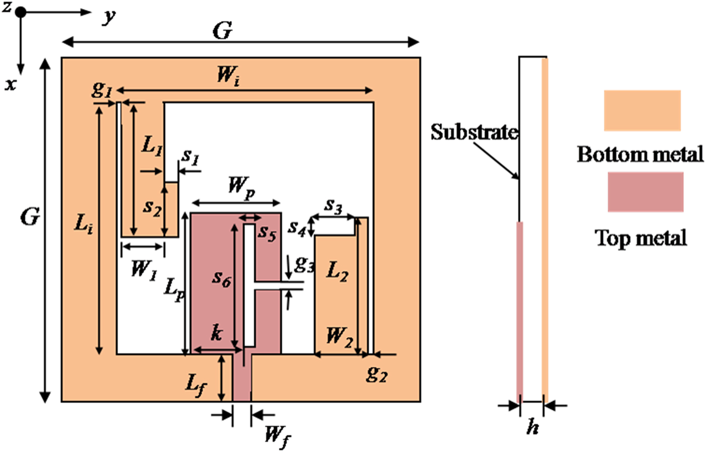
Fig. 1. Geometry of proposed antenna: (a) top view and (b) side view.
The parameters for the proposed triple-band CP antenna are listed in Table 1.
Table 1. Dimensions of the proposed antenna
Antenna prototypes
The antenna prototypes to realize the proposed antenna design is represented in Fig. 2. The overall volume G mm × G mm × h mm is constant across the design process of desired antenna. To explain the design process of this low-profile triple-band CP wide slot antenna clearly, four design steps are analyzed for the impedance bandwidth and axial ratio bandwidth (ARBW). Design 1 has only a straight x-axis-directed rectangular patch and a framed (L i × W i) lower ground. Design 2 moves the rectangular patch to negative y-direction (k) and adding a horizontal T-shaped notch on the rectangular patch from y-direction. This is a common method to achieve dual-band operation. Design 3 adds two opposite x-axis-directed strips on the ground frame for improving multiband operation with CP radiation. The proposed antenna is designed after introducing two main structures in design 3: one is the rectangular strip that is added on the x-axis-directed (left-sided) rectangular strip and the second is the rectangular slit that is cut on the negative x-axis-directed (right-sided) rectangular strip at lower ground frame.
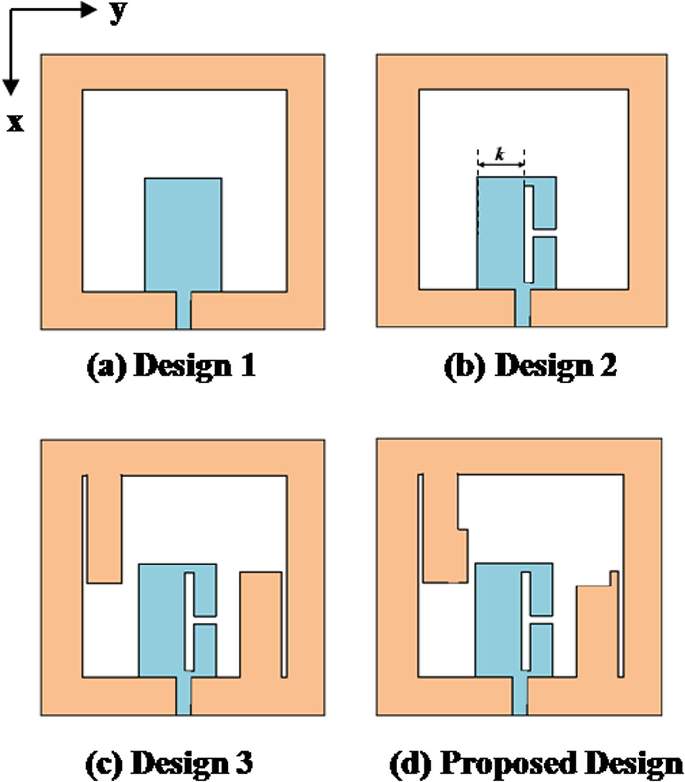
Fig. 2. Three improved prototypes with the proposed antenna.
Design simulation
Simulated results of all three prototypes with proposed antenna for return loss, axial ratio, and total gain, are discussed in this section. It is observed from Figs 3 and 4 that the designs 1 and 2 show bad return loss performance with linear polarization. The return loss performance of design 3 improved a lot in the three impedance bandwidths because the input impedance is greatly changed after adding two opposite x-axis-directed rectangular strips, and the middle ARBW is achieved. However, the lower and upper ARBWs are still poor. A small rectangular strip added on the left-sided rectangular strip and a small rectangular slit cut on the right-sided rectangular strip can significantly develop the lower and middle ARBWs. Finally, the proposed design gives triple band with improved ARBW as right-hand circular polarization (RHCP) wave for lower and middle bands with left-hand circular polarization (LHCP) wave for the upper band of the impedance bandwidth. Figure 5 shows satisfactorily total gain for desired triple band of proposed antenna.
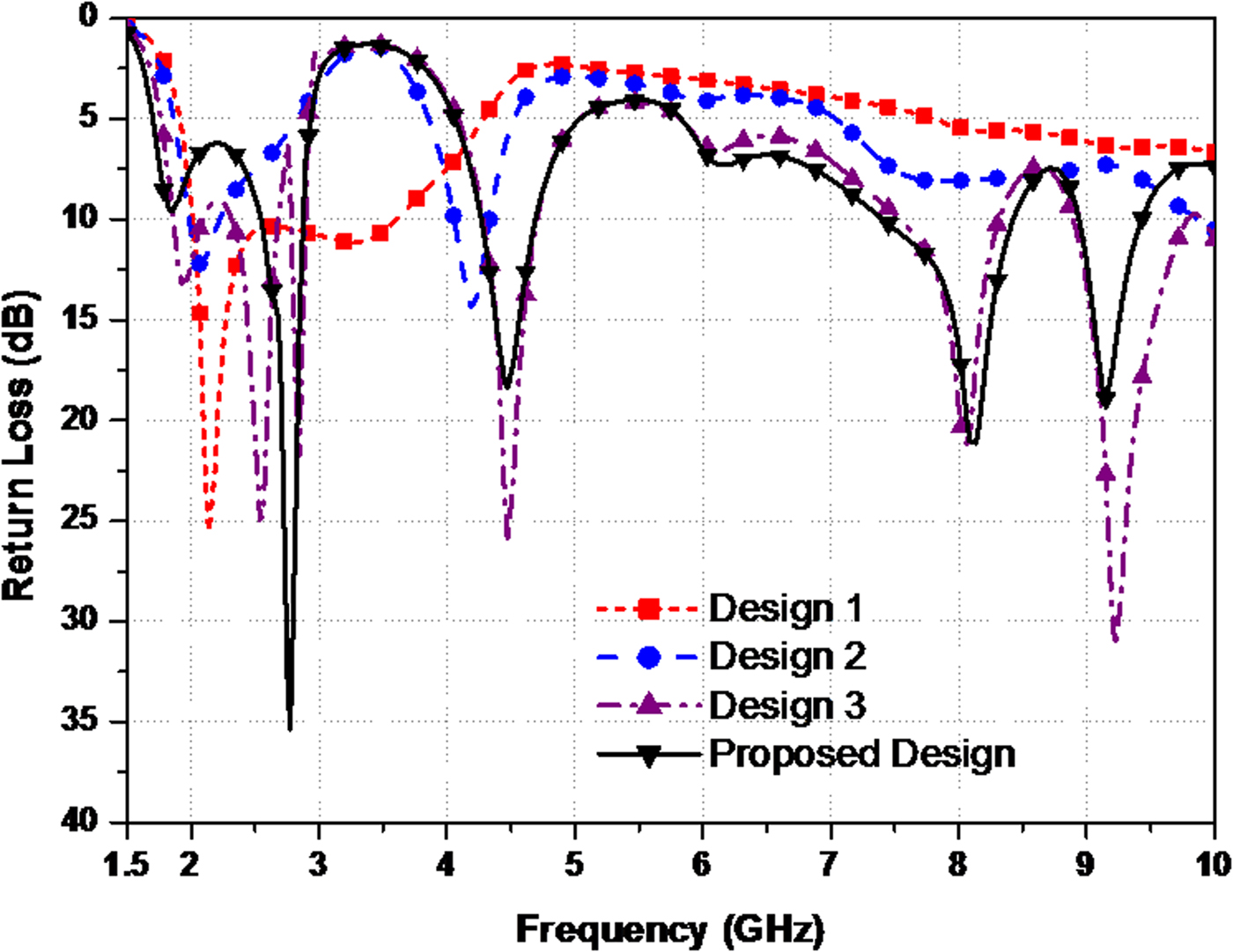
Fig. 3. Simulated results of return loss for three designs with the proposed design.
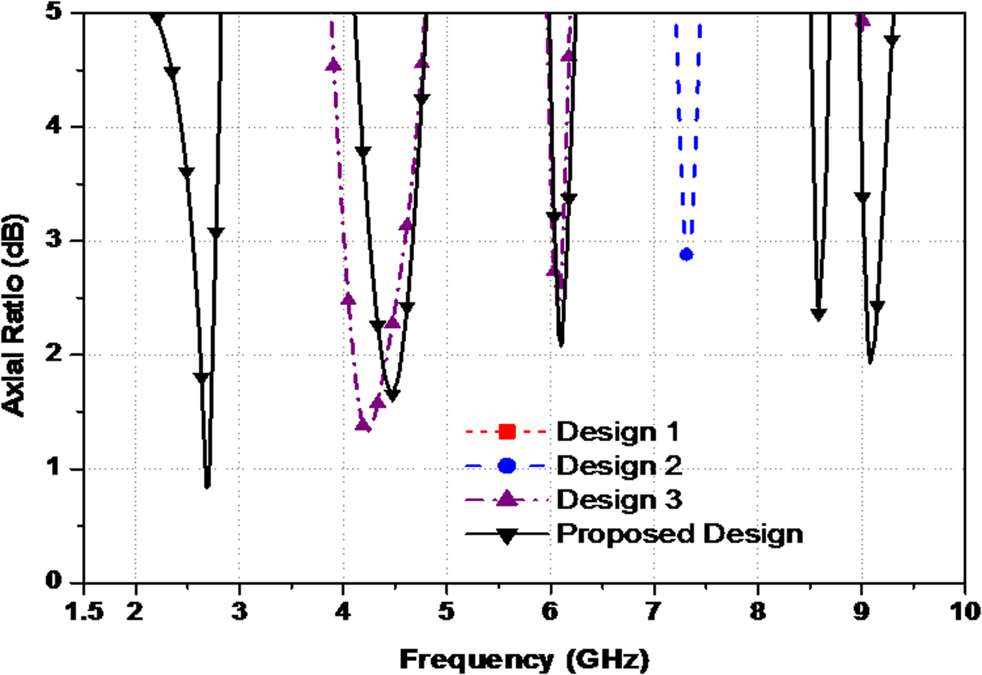
Fig. 4. Simulated results of axial ratio for three designs with the proposed design.
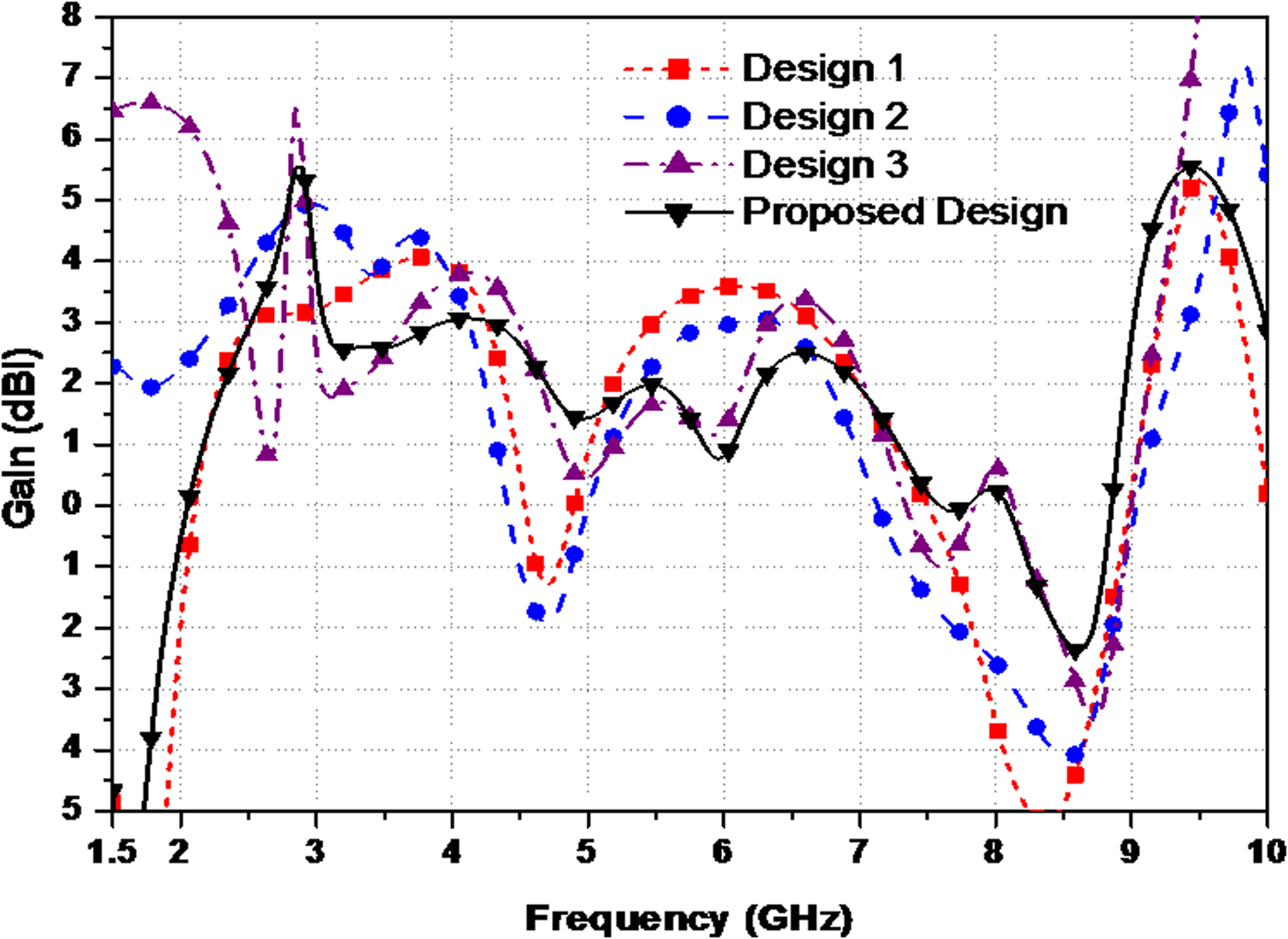
Fig. 5. Simulated results of gain for three designs with the proposed design.
Surface current distribution
To study the generation of resonant modes, surface current distributions on the antenna at 2.65, 4.45, and 9.09 GHz are presented in Fig. 6. In Fig. 6(a), maximum currents are localized mainly in the upper left corner of the slotted ground and in bottom part of the patch to produce resonant modes at 2.65 GHz. At 4.45 GHz, the bottom part of the patch mainly contributes to the resonance from Fig. 6(b). In Fig. 6(c), the maximum current is distributed mainly along the lower right corner of the ground and in a small part of the patch to excite the resonant mode at 9.09 GHz.
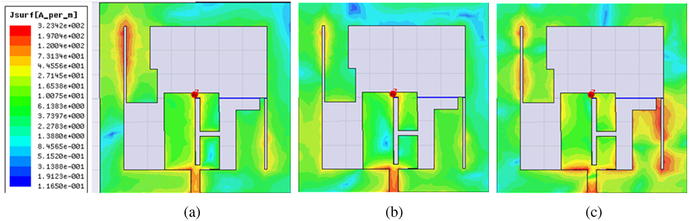
Fig. 6. Simulated surface current distributions of proposed antenna: (a) 2.65 GHz, (b) 4.45 GHz, and (c) 9.09 GHz.
Figure 7 shows the magnetic current distributions for different time phases of ωt = 0°, ωt = 90°, ωt = 180°, and ωt = 270°, at 2.65, 4.45, and 9.09 GHz, respectively. Two orthogonal resonant modes with a 90° phase difference and equal amplitude can realize CP radiation. It signifies the direction of the magnetic current vector at time phases ωt = 0° and 90°, which are equal in magnitude and opposite to time phases 180o and 270o, respectively. As shown in Figs 7(a) and 7(b), it can be observed that the combined effect of magnetic current vectors of a notched patch and ground plane gives CP wave rotation in the right-hand direction for the first and second bands, at 2.65 and 4.45 GHz, respectively; whereas the simulated magnetic current vectors of the proposed antenna in Fig. 7(c) give CP wave rotation in the left-hand direction for the third band, at 9.09 GHz.
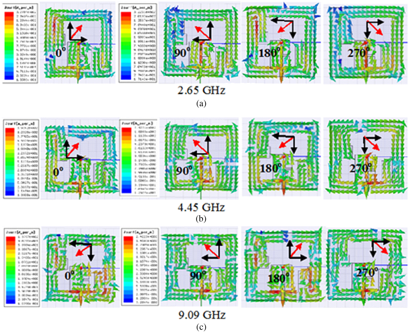
Fig. 7. Simulated magnetic current distributions for 0 and 90o: (a) at 2.65 GHz, (b) at 4.45 GHz, and (c) at 9.09 GHz.
Parametric analysis
In this section, a parametric analysis of the proposed antenna for further study was conducted. The results provide a useful guideline, to achieve desired operating bands with CP radiation. To know the effect of antenna parameters in the parametric analysis, at a time, only one parameter was varied, while other parameters were kept constant.
First studied parameters are the left rectangular small strip (s 1 × s 2) at the lower ground. Figure 8 shows the influence on return loss and axial ratio with the increase of s 1. As shown in the figure, s 1 has no effect on return loss. However, the influence on the axial ratios is considerable. By varying s 1 from 1 to 1.5 mm, the first two ARBWs are significantly changed from 2.77–2.84 to 2.56–2.7 GHz and 4.19–4.68 to 4.12–4.54 GHz, respectively. The ARBW becomes poor with the further increase of s 1 from 2 to 2.5 mm. Figure 9 shows the influence on return loss and axial ratio with the increase of s 2. The variation of length s 2 has no effect on return loss. However, the influence on the axial ratio is drastic. The second ARBW becomes wider with the increase of s 2 from 6 to 8 mm.

Fig. 8. Effects of varying s 1 on return loss and axial ratio.
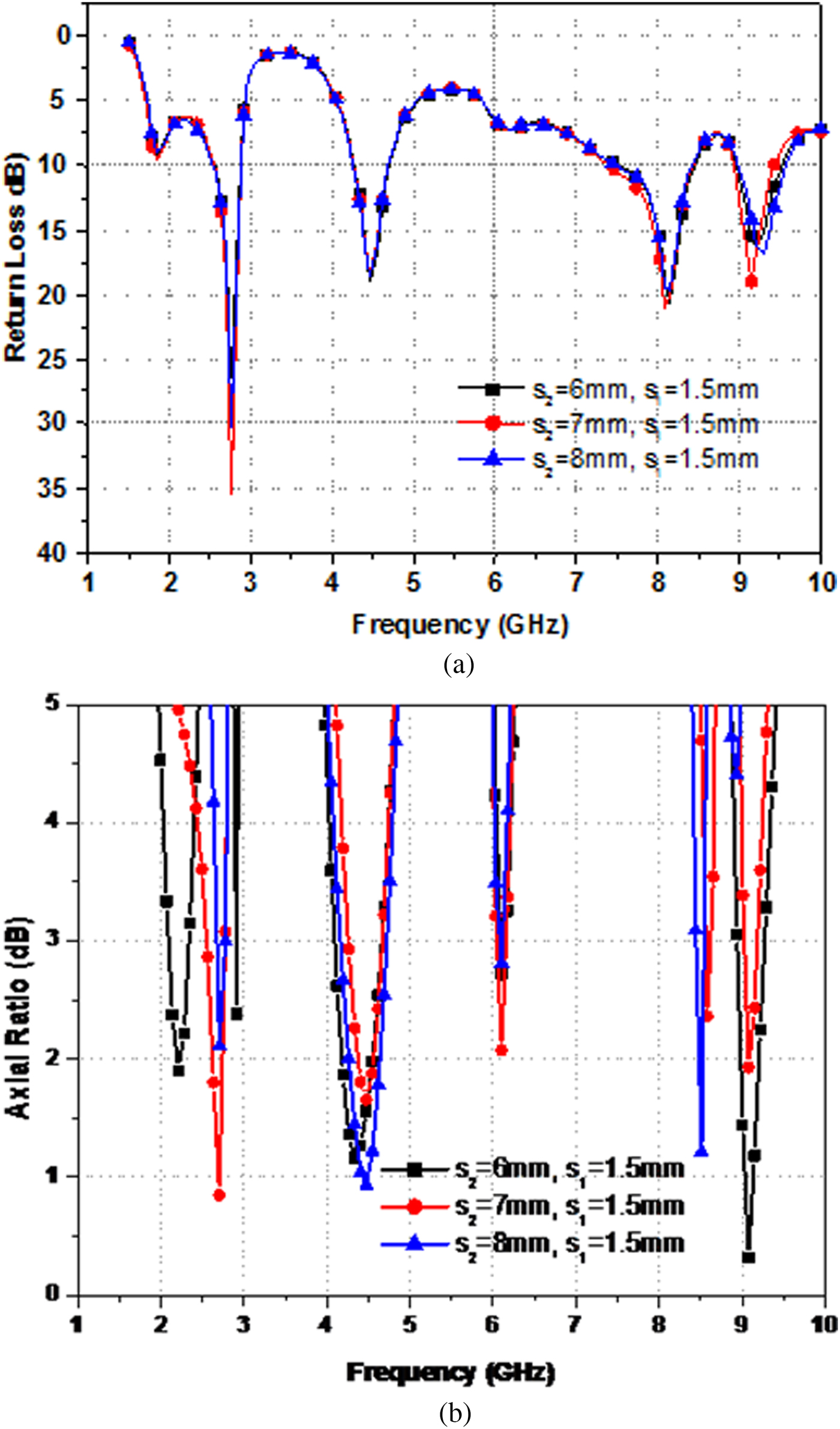
Fig. 9. Effects of varying s 2 on return loss and axial ratio.
Now, the second studied parameters are the right rectangular small slit (s 3 × s 4) at the lower ground. The effects of the length s 3 on the impedance bandwidth and ARBW are presented in Fig. 10. As shown in Fig. 10, s 3 has influence on both return loss and axial ratio. When s 3 increases, the last impedance bandwidth is shifted toward the upper frequencies. In Fig. 11, the effects of s 4 on return loss and axial ratio for the proposed antenna are also investigated. It is found that s 3 and s 4 play an important role in circular polarization property of the antenna. As shown in Fig. 11, significant improvement of the axial ratio is observed by tuning s 4 and s 4.
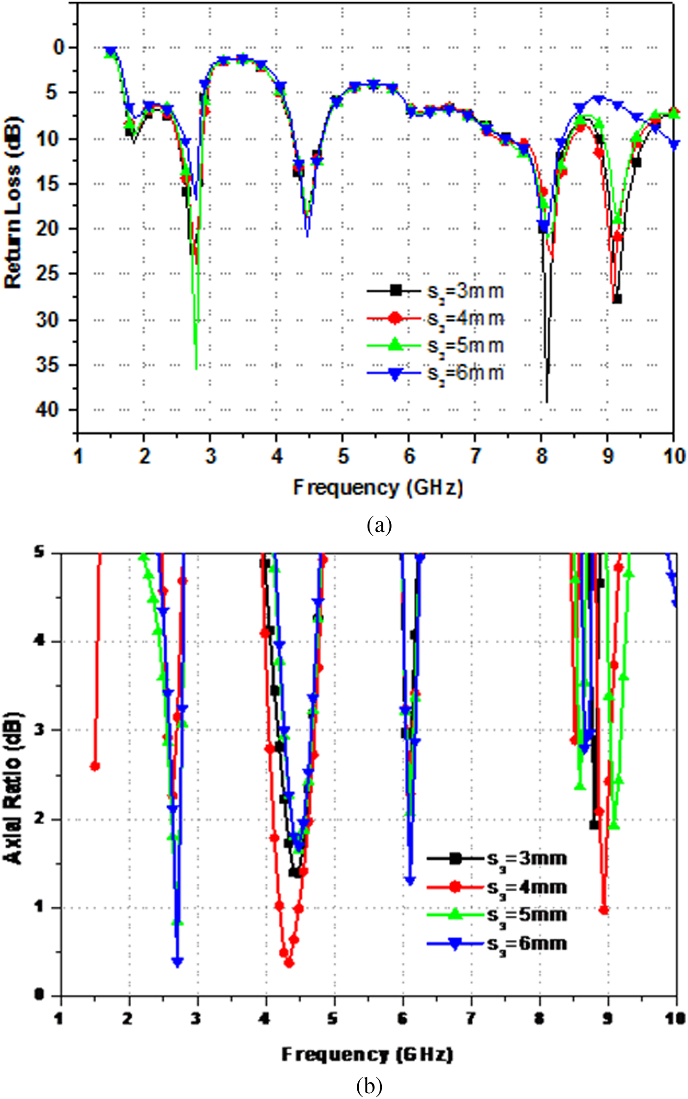
Fig. 10. Effects of varying s 3 on return loss and axial ratio.
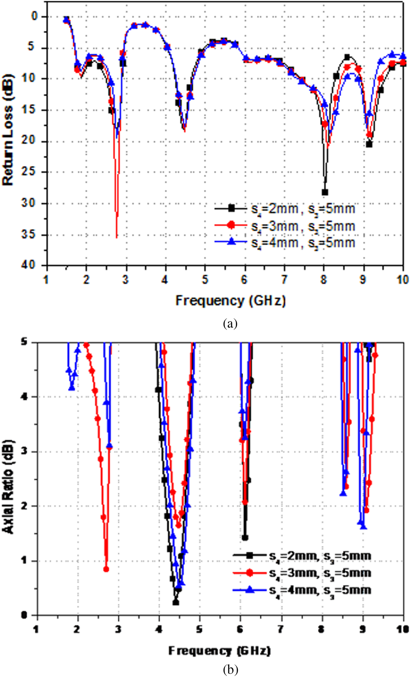
Fig. 11. Effects of varying s 4 on return loss and axial ratio.
Experimental results and discussion
This section explained the experimental results of the proposed antenna. Based on the optimized parameters, the antenna is fabricated and measured. The designed antenna has a total size of 40 mm × 40 mm × 1 mm that operates over triple impedance bandwidth of 340, 430, and 490 MHz. The 3 dB ARBWs are 200, 400, and 150 MHz, respectively, corresponding to the appropriate resonant frequencies over the three operating bands.
Fabricated antenna
The proposed antenna is fed using 50 Ω SMA connector placed along the microstrip feed line. The fabrication of proposed antenna is complete with optimized parameters, and measurement has been performed with the help of Agilent™ vector network analyzer of PNA-L series. The image of top and bottom views of the fabricated triple-band CP wide slot antenna prototype are shown in Figs 12(a) and 12(b).
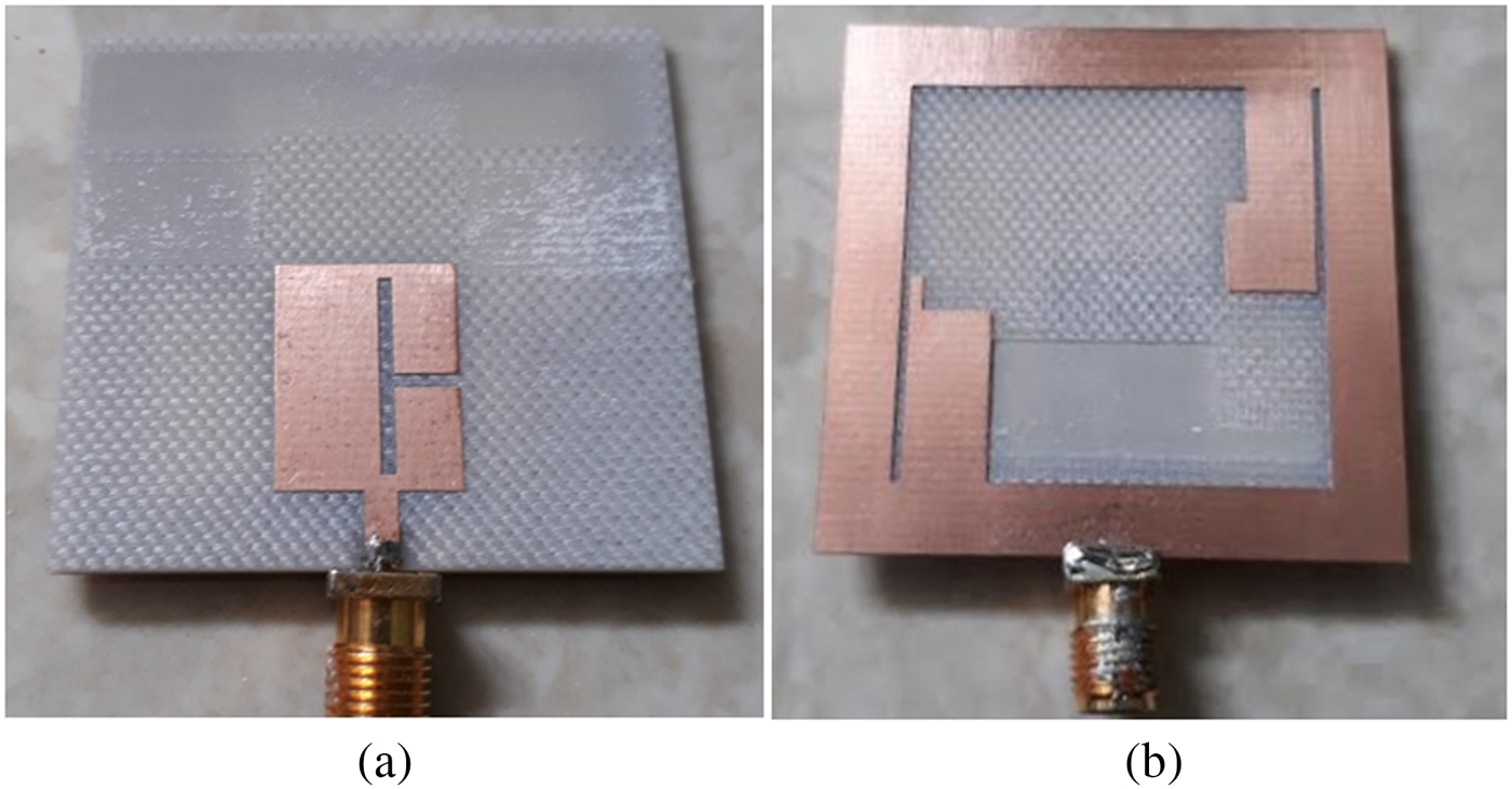
Fig. 12. Fabricated image of the proposed antenna: (a) top view and (b) bottom view.
Return loss and axial ratio
The results of the proposed triple-band CP wide slot antenna are discussed in this section. Figure 13 shows the variation of return loss with the frequency of the designed antenna. It is clear from the result that the antenna operates in a triple frequency band which is from 2.56 to 2.9 GHz for the first band, from 4.25 to 4.68 GHz for the second band, and from 8.93 to 9.42 GHz for the third band. Measured center frequencies have more than −10 dB return loss and are 2.73, 4.46, and 9.18 GHz for the first, second, and third bands, respectively. Due to the single-feed structure, a spurious resonant mode is generated at 8.18 GHz. This resonant mode is discarded, because of lack of gain and desired 3 dB ARBW. Furthermore, Fig. 14 shows the plots of measured and simulated ARBW against frequency. The measured result shows the 3 dB ARBW of about 200 MHz (2.55–2.75 GHz), 400 MHz (4.25–4.65 GHz), and 150 MHz (9.02–9.17 GHz) at center frequencies of 2.65, 4.45, and 9.09 GHz, respectively. It seems that the simulated results agree reasonably well with the measured results.

Fig. 13. Variation of return loss with frequency.
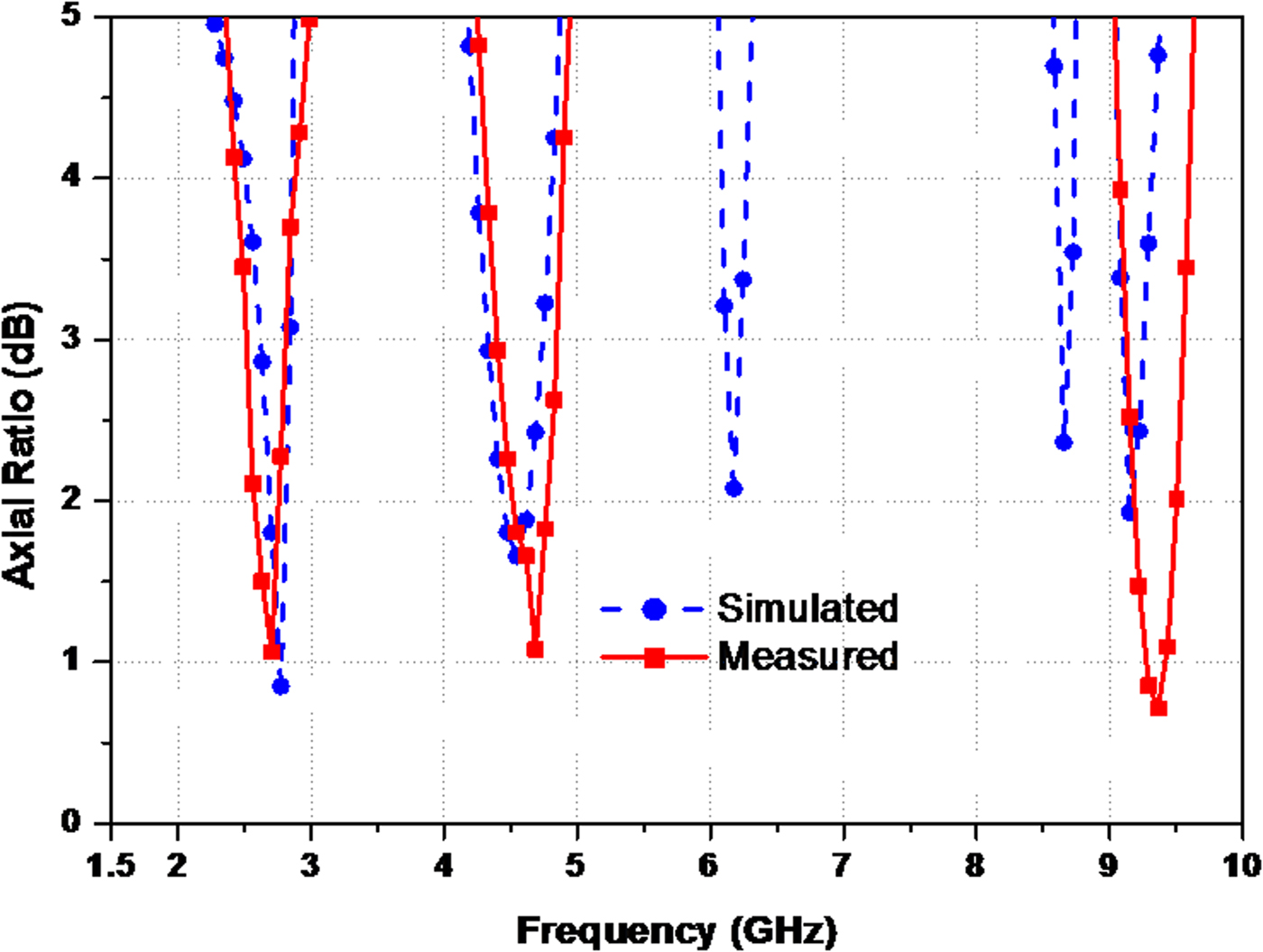
Fig. 14. Variation of axial ratio with frequency.
Gain, radiation efficiency, and radiation pattern
Figure 15 shows an excellent agreement between the plots of measured and simulated total gain against frequency. It is observed that the antenna having highest peak gain of 3.03, 3.5, and 5.64 dBi at 2.65, 4.45, and 9.09 GHz center frequencies of CP band, respectively. Figure 16 gives the simulated and measured antenna efficiency performance of the triple-band CP antenna. The antenna efficiency is about 83% over the desired operating bands.
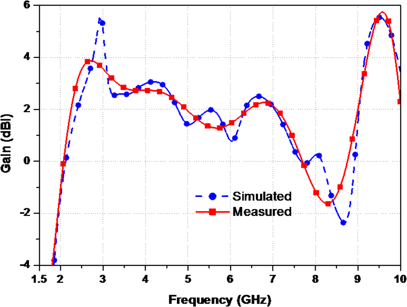
Fig. 15. Variation of gain with frequency.
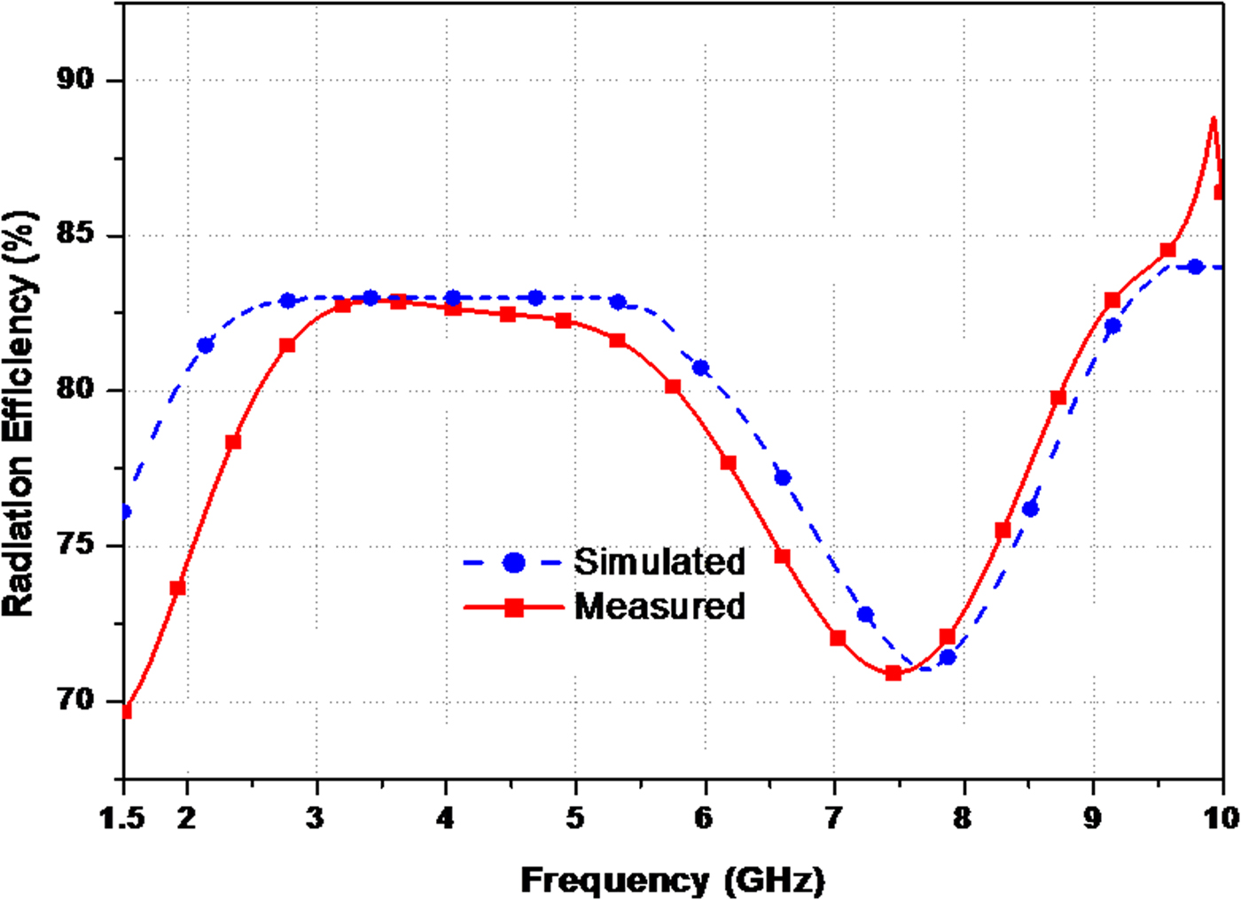
Fig. 16. Variation of radiation efficiency with frequency.
Radiation pattern of the proposed antenna in the xz- and yz-planes at 2.65, 4.45, and 9.09 GHz are shown in Figs 17(a)–17(c), respectively. The close observation of radiation pattern for desired operating triple frequencies illustrates that the RHCP wave is generated in the first two bands and LHCP wave in the third band. Almost boresight radiation patterns are observed at the lower and middle bands; however, the patterns at the upper band show a slight deviation from the broadside direction. This is mainly due to the effect of the currents on the lower right corner of the ground plane. The half-power beam-width (−3 dB) of the antenna in the xz- and yz-planes at 2.65 GHz are 57 and 75° (from −21 to 36° and from −34 to 41°°), at 4.45 GHz are 86 and 75° (from −46 to 40° and from −45 to 30°), and at 9.09 GHz are 17 and 52° (from −6 to 11° and from −48 to 4°).
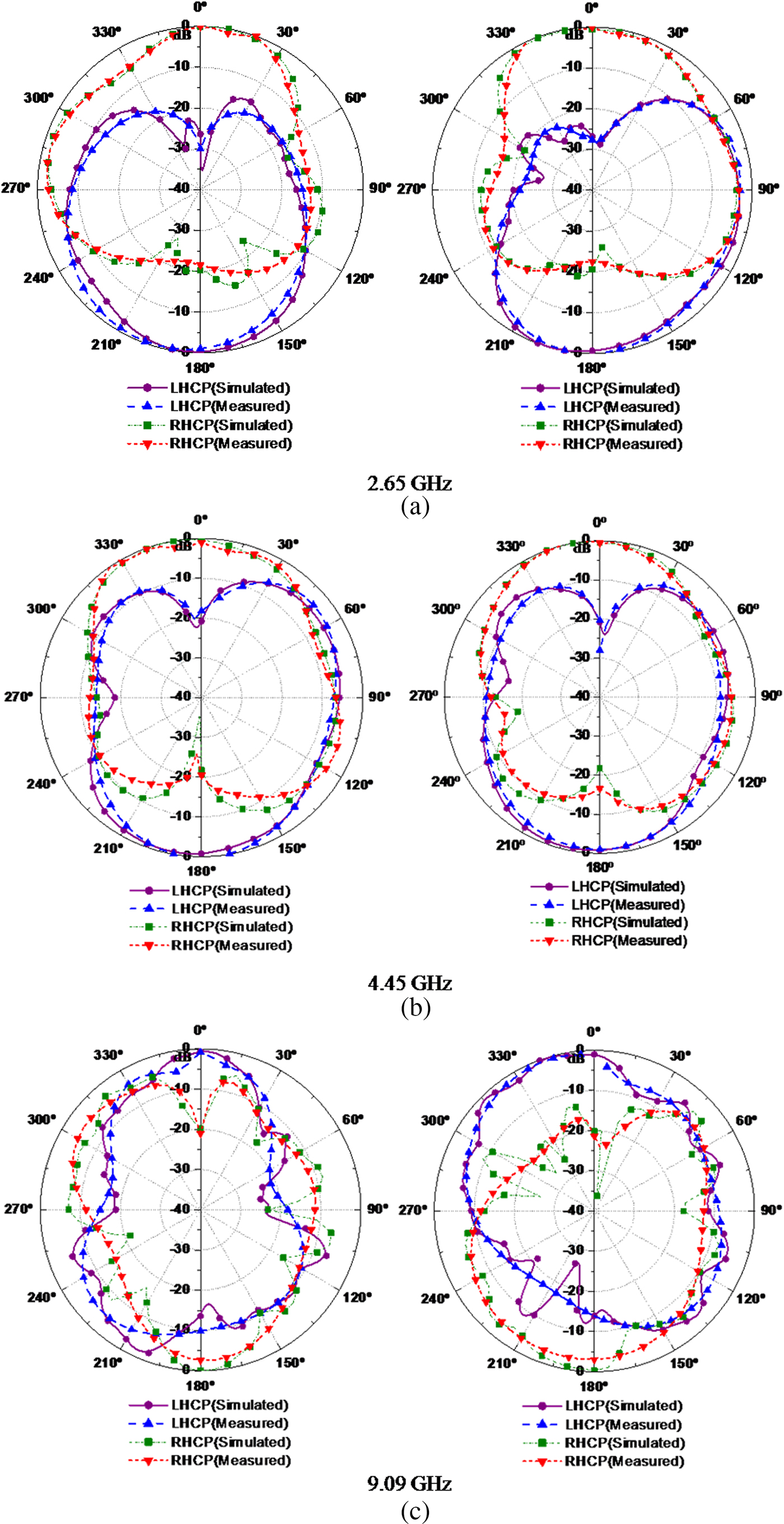
Fig. 17. Simulated and measured radiation pattern in the xz- and yz-planes: (a) at 2.65 GHz, (b) at 4.45 GHz, and (c) at 9.09 GHz.
To conclude the senses of the two CP waves, the left-hand and the right-hand components at all three frequencies are measured and are recorded in Fig. 17. At 2.65 and 4.45 GHz, the RHCP component is more than 20 dB higher than the LHCP component in the bore sight direction on the xz- and yz-planes. Otherwise, at 9.09 GHz, the LHCP component is more than 20 dB higher than the RHCP component in the bore sight direction on the xz- and yz-planes. As a result, the antenna radiates RHCP in the bore sight direction, at 2.65 and 4.45 GHz, and LHCP in the bore sight direction, at 9.09 GHz. The results of simulated radiation patterns are validated by comparing them with measured radiation patterns, to demonstrate the stability of radiation patterns at all three considered frequency. The simulated and measured results show good agreement between them. Minor differences shown in the simulated and measured results are due to the fabrication imperfections and measurement errors.
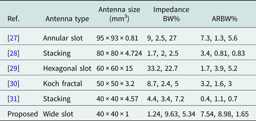
Table 2 illustrates the comparison of proposed triple-band triple-sense CP antenna and the previous triple-band CP antennas. It shows that this antenna has a simpler structure, more compact size, and good impedance bandwidths with suitable ARBWs.
Table 2. Comparison of triple-band circularly polarized antennas

Conclusion
A microstrip-fed, rectangular patch loaded with T-shaped notch, wide slot antenna featured for triple-band CP has been designed and successfully implemented. The simulated antenna structure is quite capable in producing three frequency bands with desired 3 dB ARBWs. The measured gains are comparatively stable across all three CP bands. From the measured and simulated results, it is observed that the proposed antenna offers higher isolation between adjacent bands with good radiation pattern characteristics. The results obtained by simulation are acceptable with measured results. In addition with the feature of a simple and compact topology, the antenna is low-cost and is suitable for multi-band wireless communication.
 Shilpee Patil received her B.Tech. degree in Electronics and Communication Engineering from AKTU (formerly UPTU), Lucknow, India, and the M.Tech. degree in Digital Communication from GGSIP University, Delhi, India, in 2009. She is currently pursuing her Ph.D. degree in Electronics Engineering from AKTU, Lucknow, India. Her research interests are microstrip antennas, slot antennas, and circularly polarized microstrip antenna for wireless communications.
 Anil Kumar Singh was born in Jamalpur, Mirzapur (UP), India in 1976. He completed his M.Tech. degree in Instrumentation and Control Engineering from NITTTR Chandigarh, India, and Ph.D. degree on Some Study on Annular Ring Microstrip Antenna from Electronics Engineering Department, Indian School of Mines (ISM), Dhanbad, India. He joined the Department of Electronics and Instrumentation Engineering, Institute of Engineering and Technology, M. J. P. Rohilkhand University, Bareilly, India, as a Lecturer in 2002. He has published more than 20 papers in national and international journals and conferences. His current research interest includes design and analysis of microstrip antennas.
 Binod Kumar Kanaujia is working as a Professor in the School of Computational and Integrative Sciences, Jawaharlal Nehru University, New Delhi since August 2016. Dr. Kanaujia had completed his B.Tech. in Electronics Engineering from KNIT, Sultanpur, India, in 1994. He did his M.Tech. and Ph.D in 1998 and 2004, respectively, from the Department of Electronics Engineering, I.I.T. B.H.U., Varanasi, India. He has keen research interest in design and modeling of reconfigurable and circular polarized microstrip antenna. He has been credited to publish more than 150 research papers with more than 430 citations with h-index of 12 in peer-reviewed journals and conferences. He had successfully executed four research projects sponsored by several agencies of Government of India, i.e. DRDO, DST, AICTE, and ISRO. He is a member of several academic and professional bodies, i.e. IEEE, Institution of Engineers (India), Indian Society for Technical Education, and Institute of Electronics and Telecommunication Engineers of India.
 R. L. Yadava is working as a Professor in the Department of Electronics and Communication Engineering, Galgotias College of Engineering and Technology, Greater Noida, Uttar Pradesh India. He received his Ph.D. degree in Electronics Engineering from I.I.T. B.H.U., Varanasi, India. He joined Vellore Institute of Technology (VIT) University, Vellore, India, in 2001 and served as Head of the Microwave Division, Coordinator (R&D) and Coordinator (UG) of Electrical Sciences. He has organized several guest lectures, short-term training programs and conferences in the field of microwave and antennas. His research areas include waveguides, microwaves, and microstrip antennas. Presently, he is working on fractal antennas, superstrate-loaded and AFFS antennas, and RECTENNAS in collaboration with ISM DHANBAD and other reputed universities. He has 65 publications to his credit in international/national journals, conferences, and symposiums. He is an Associate Editor of Journal of Information, Intelligence and Knowledge, USA and also a member of ISTE, STE, SEMCE(I), and IEEE.