I. INTRODUCTION
Recently, the demand for phased array systems has been steadily increasing [Reference Parker and Zimmermann1], particularly for emerging millimeter (mm)-wave applications, such as 5 G, 60 GHz Wi-Fi, automotive radar, and land mobile satellite communication. The electronic beam-scanning capability is the major advantage of the large-scale phased array antennas. However, this capability requires a high-cost, high-power consumption, and complex feeding network with a large number of tuning elements such as phase shifters, amplifiers, and switches. The phase shifter is the most critical element and the bottleneck toward reducing the cost and the complexity of the phased array system and significantly enhances the performance of such systems. There are many factors that are used to evaluate a phase shifter. Phase shift variation range, insertion loss, insertion loss variation, size, cost, speed, integration, bandwidth, passivity, and high-power handling are the most crucial properties that should be considered in the choice of the phase shifter [Reference Norvell, Hancock, Smith, Pugh, Theis and Kriatkofsky2, Reference Wu3].
The phase shifters are typically divided into analog and digital types. Despite their main attractive feature, namely their accurately predictable phase shift, digital phase shifters are a suitable choice only for applications that require discrete phase shift and for which power consumption is not a concern. The most desirable characteristics of a phase shifter, particularly for large phased array applications, include low insertion loss, low insertion loss variation, wide operating frequency band, compact size, and reciprocity. Such phase shifters are key elements for realizing a low-cost, low-power consumption, and low-complexity phased array antenna. In particular, for a mm-wave-phased array system with (0.5 λo×0.5 λo) cell size, it is quite important that the phase shifter has such a small footprint that it can be placed directly underneath the antenna element and share the power amplifiers and low-noise amplifiers among a group of antennas. Furthermore, these characteristics facilitate antennas and phase shifters to be shared between the transmitter and the receiver, thereby highly reducing the cost, power consumption, complexity, and the size of the phased array systems [Reference Norvell, Hancock, Smith, Pugh, Theis and Kriatkofsky2, Reference Pillans, Coryell, Malczewski, Moody, Morris and Brown4]. Therefore, a low-cost, compact, and integrated phase shifter with minimal insertion loss variation is essential for high-performance telecommunication phased array systems.
Micro-electro-mechanical systems (MEMS)-based phase shifters are mainly of digital type. The analog MEMS phase shifters are large and show a low figure of merit (FOM) [Reference Pillans, Coryell, Malczewski, Moody, Morris and Brown4–Reference Chicherin, Sterner, Lioubtchenko, Oberhammer and Räisänen7]. Passive-type monolithic microwave-integrated circuit phase shifters suffer from high insertion loss, limited resolution, and limited operating bandwidth [Reference Shin8–Reference Lambard, Lafond, Himdi, Jeuland and Bolioli12]. An alternative approach is to use tunable dielectric-based phase shifters such as ferroelectrics [Reference De Paolis, Payan, Maglione, Guegan and Coccetti13–Reference Zhao, Wang, Choi, Lugo and Hunt16], and liquid crystal (LC) [Reference Jost17–Reference Bulja, Mirshekar-Syahkal, James, Day and Fernández19]. These materials have dielectric properties that change when exposed to an electric field, causing a phase change. All the aforementioned phase shifters can potentially be low cost, and compatible with planar circuits. However, they show a low FOM performance <50°/dB especially at the frequency bands of interest. Additionally, ferroelectric-based phase shifters show a poor return loss–phase relation over the operating frequency bandwidth [Reference Zhao, Wang, Choi, Lugo and Hunt16], and phase shifters based on common LC materials suffer from slow response to the applied electric field [Reference Jost17]. Adding a perturber to the top of a planar transmission line and using a mechanical actuator to change the phase shift [Reference Wu3, Reference Romano, Araromi, Rosset, Shea and Perruisseau-Carrier20–Reference Kim, Yun and Chang23] is the basis of another type of continuous phase shifter. Among these, elastomer-based phase shifters require a very high biasing voltage [Reference Romano, Araromi, Rosset, Shea and Perruisseau-Carrier20] and the device occupies a large area. A metallic perturber, used in [Reference Wu3], generates a large-phase shift variation and reduces the size of the device. However, the insertion loss rapidly increases with frequency. Furthermore, the measured insertion loss variation is substantially high. In [Reference Kim and Chang21, Reference Kim, Yun and Chang23], a low dielectric slab is used to tune the phase of a planar transmission line, but the length of the device should be sufficiently large to achieve the required phase shift, also the insertion loss increases with frequency. Similarly, phase shifters using a magneto-dielectric disturber suffer from large size and high insertion loss at high frequency [Reference Yang and Sun22].
As a highly promising response to these challenges, the authors presented a novel low-loss phase shifter based on very high dielectric constant materials, such as Barium Lanthanide Tetratitanates (BLT) ceramics in [Reference Abdellatif24] and [Reference Abdellatif25]. Based on this new concept, low insertion loss and compact phase shifters with minimal insertion loss variation have been developed. The phase shifter consists of a coplanar waveguide (CPW) line on a high resistivity silicon substrate loaded by a BLT rectangular slab. By changing the gap between the CPW and BLT, the propagation constant of the CPW mode is perturbed causing a substantial change in phase. Among the proposed designs, the CPW-serpentine line loaded with BLT slab is more compact and offers higher phase shift ~369° at 30 GHz. However, it suffers from impedance mismatches that limit the operating frequency bandwidth, especially when it is loaded by a BLT slab with high dielectric constant εr > 100. To solve this problem, the BLT slab is tapered from both ends to minimize reflections [Reference Abdellatif25]. Although this technique is successful in enhancing the operating bandwidth (more than 20 GHz), it degrades the phase shifter dynamic range and increases the complexity of the fabrication process. Moreover, due to the use of non-standard-fabrication methods, the proposed designs in [Reference Abdellatif24] and [Reference Abdellatif25] might not be suitable for high-volume low-cost phased array systems.
In this paper, a more cost-effective approach is proposed for the phase shifter, particularly for large-scale mm-wave phased arrays. The proposed phase shifter is simple, compact, and easy to integrate to the array beam-forming network. For demonstration, it is designed for two-way Ka-band satellite communication (downlink from 19 to 21 GHz and uplink from 28.5 to 30.50 GHz). Moreover, an experimental demonstration of voltage–phase control is presented at both frequency bands. No geometry scaling, matching/transition techniques are required over the entire tuning range in both operating frequency bands. Inspired by the approach presented in [Reference Abdellatif24], a small dielectric slab made of ceramic material covers a grounded coplanar waveguide (GCPW) structure. The GCPW's gap line is modified under the dielectric slab to overcome the mismatch limitation of the previous design.
II. DESIGN
A) Phase shifter analysis
Since the phase shifter will be integrated into the antenna element that has 5 mm×5 mm area at 30 GHz, this area should house the proposed phase shifter and part of the feed circuit. This area is set as the upper bound of maximum size obviously; we try to make the phase shifter smaller than this limit to facilitate circuit assembly and packaging. On the other hand, the lower bound on the size of the phase shifter is limited by the required phase variation, which is 360°.
The physical values of the proposed phase shifter can be obtained based on the area assigned for the phase shifter, maximum phase variation, and dielectric permittivity of the BLT slab. The design steps can be summarized as follow:
1. The trace width and the gap of the 50 Ω GCPW line are calculated at the operating frequency.
2. Calculating the thickness and the length of the dielectric slab to achieve 2π phase shift variation based on equation (1).
3. Full-wave simulation to evaluate the performance of the phase shifter.
4. Routing the GCPW line under the BLT slab within the assigned physical area to facilitate the maximum physical length of the GCPW line within assigned area to maximize the achievable phase shift variation.
5. Modification of the GCPW gap size under the BLT slab to improve the impedance matching of the proposed phase shifter due to the effect of BLT slab proximity to the GCPW line.
6. Fabrication and measurement to validate the theoretical results.
A full-wave simulation using high frequency structure simulator (HFSS) was used to develop a simple analytical formulation between the phase shifter performance and its physical dimensions. Accordingly, we found that a simple formula extracted (equation (1)) to predict the maximum phase variation of the proposed phase shifter with return loss <10 dB over the operating frequency band and minimum insertion loss. In this analysis, the air gap size is limited to 1–10 µm, which is the displacement range of the piezoelectric transducer (PET).
 $$\Delta \emptyset _{max} = k \times L_s \times \sqrt {\varepsilon r}, $$
where  $\Delta \emptyset _{max} $ is the maximum phase shift variation at design frequency 30 GHz, K is the proportionality constant, which depends on the dielectric slab thickness (h s), L is the dielectric slab length in mm, and εr is the dielectric permittivity of the BLT slab.
Dielectric slab thickness is chosen to maximize the phase shift variation with minimum insertion loss over the operating frequency h s = 0.13 × λg slab where  $\lambda g_{slab} = (c/f \times \sqrt {\varepsilon _r} ).$ Figure 1 shows the phase shifter circuit used to validate the extracted design equation. In this simulation, a BLT slab with 1 mm width and thickness of hs = 0.13×λg slab at 30 GHz, is used with a 50 Ω GCPW line.
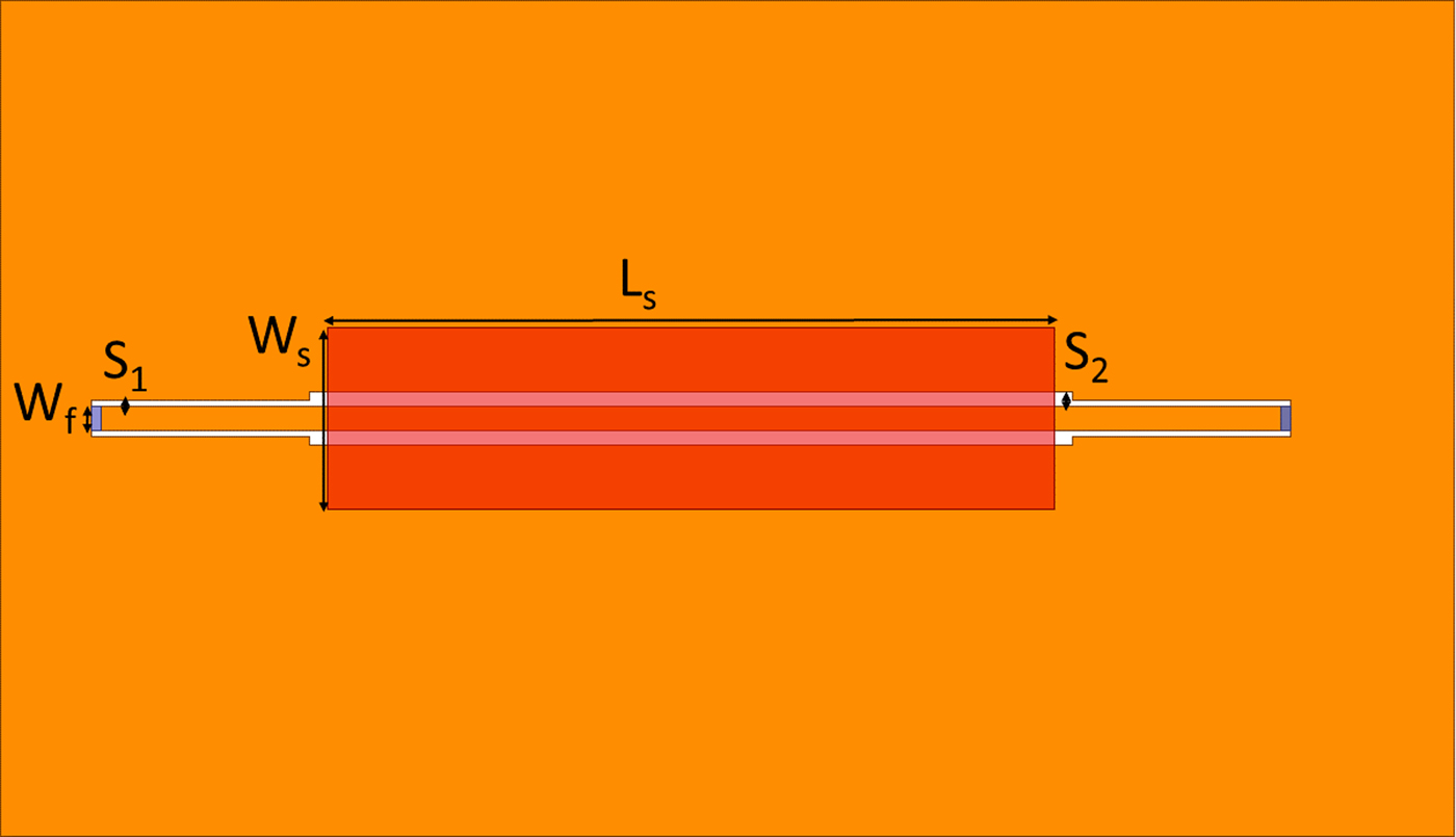
Fig. 1. Phase shifter structure labeled with the design parameters W f = 0.14 mm, S 1 = 0.03 mm, S 2 = 0.1 mm, W s = 1 mm.
The BLT dielectric permittivity is varied between 40 and 80, and the length varied between 3 and 4 mm. The air gap between the BLT slab and the GCPW line is varied between 1 and 10 µm. The simulation results of the phase–gap relation of different cases are shown in Fig. 2.
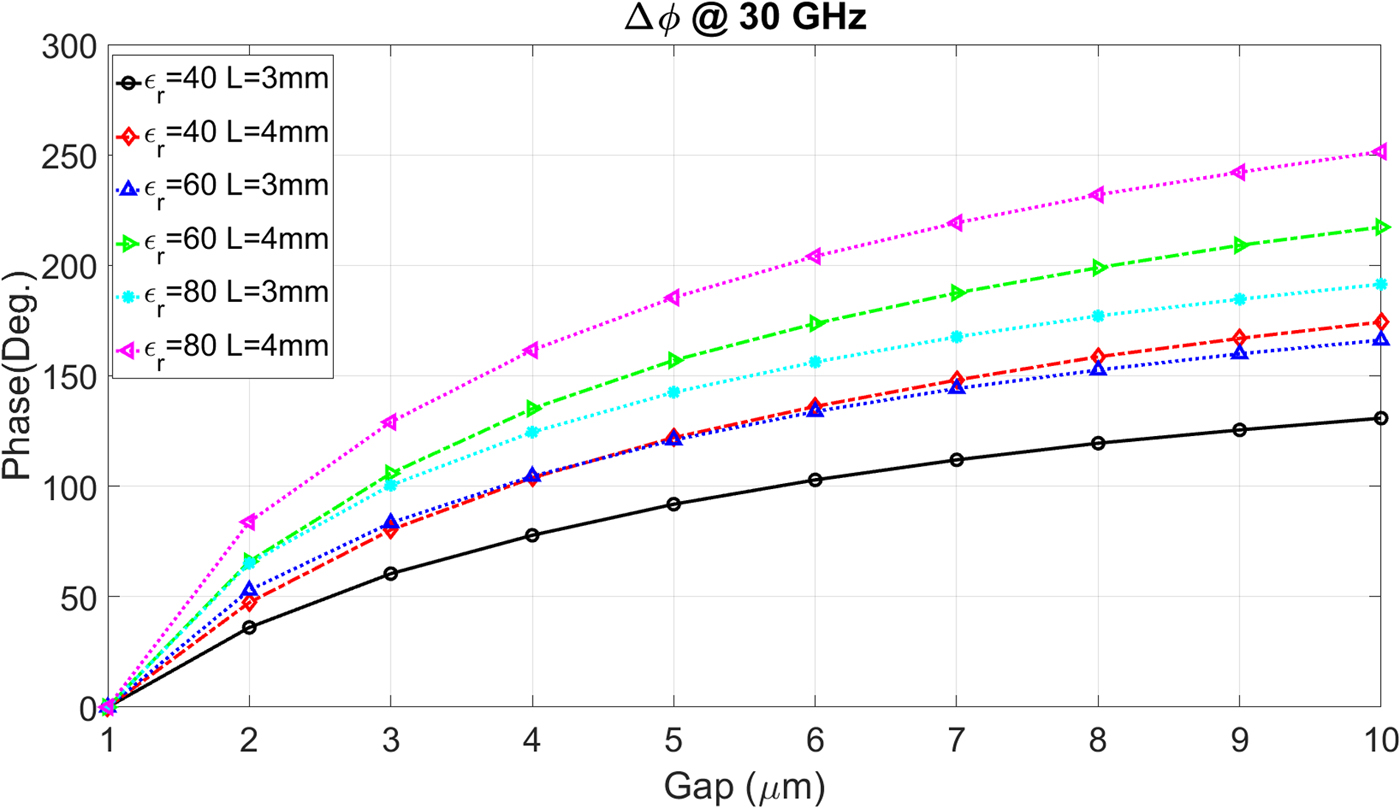
Fig. 2. Phase shifter simulation results with different dielectric permittivity and slab length.
Table 1 compares the analytical maximum phase variation versus the full-wave results. The analytical formula predicted the maximum phase variation accurately within ±2% variation.
Table 1. Comparison of analytical maximum phase variation with the simulation results.

B) Meander line-based phase shifter
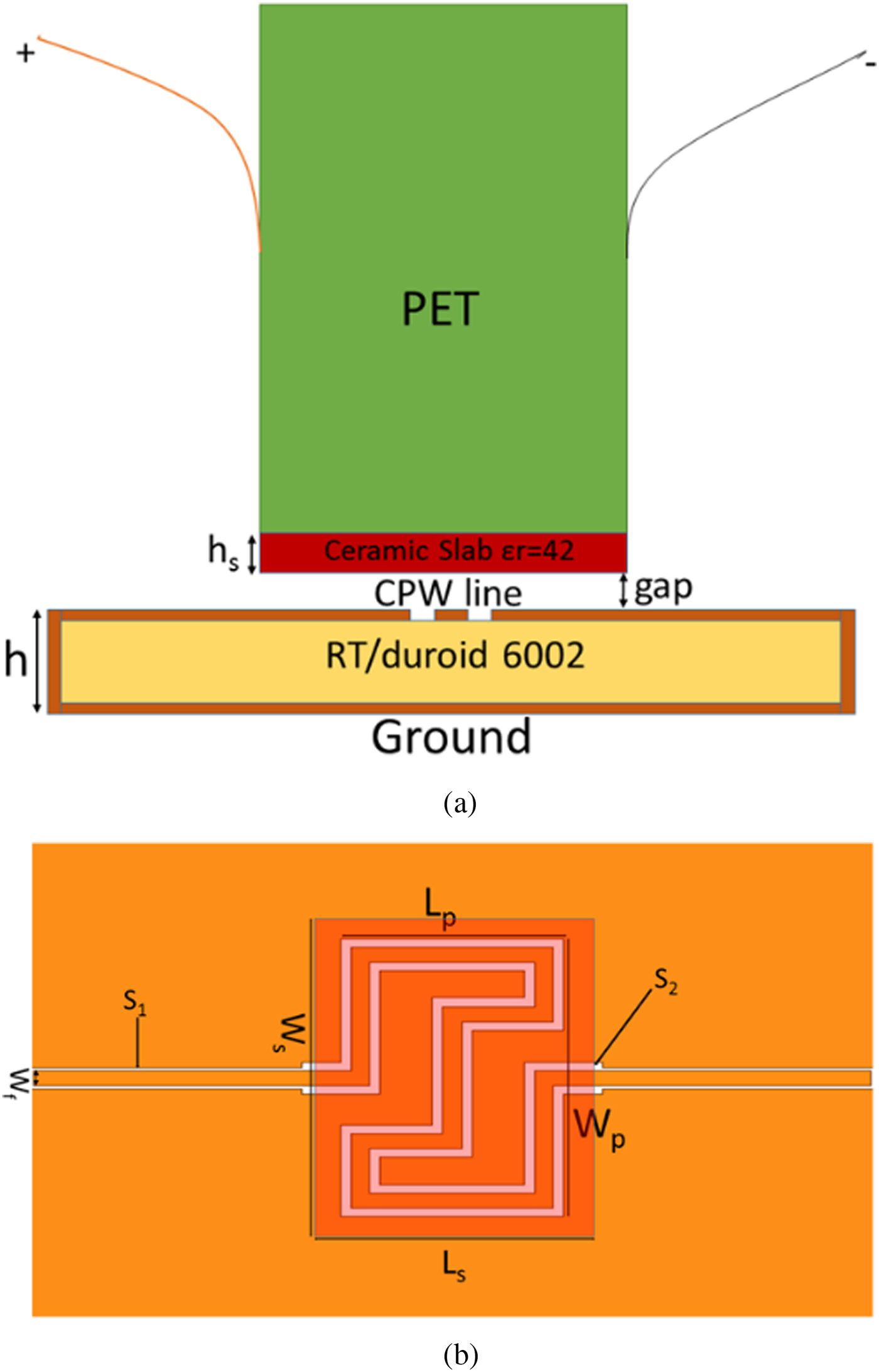
The proposed phase shifter prototype consists of a high dielectric ceramic slab that is placed on the top of the GCPW line with a tunable height (gap) as shown in Fig. 3(a). As a proof of concept, a PET controls the air gap between the dielectric slab and the GCPW line. The GCPW line is designed on RT/duroid 6002, which has an electric permittivity ε r = 2.94, tanδ = 0.0012, and 35 µm copper thickness. The sidewalls of the substrate are plated to ensure an electrical connection between the top and the bottom grounds of the GCPW line. The substrate is light, easy to fabricate and integrate within multilayer printed circuit board (PCB) feeding networks. The other advantage of using a low dielectric constant substrate in the proposed design is that it creates a high contrast between the GCPW substrate and the dielectric slab. This contrast makes the phase shift more sensitive to the air gap variation, thereby increasing the dynamic range of the phase shifter. The relative phase shift is varied as a function of the gap height.

Fig. 3. Proposed phase shifter structure labeled with the design parameters: h = 0.5 mm, W f = 0.14 mm, S 1 = 0.03 mm, S 2 = 0.1 mm, L p = 1.7 mm, W p = 2.6 mm, L s = 2.1, W s = 3 mm, h s = 0.2 mm. (a) Cross-section of the proposed phase shifter. (b) Top view of the GCPW and the BLT slabs.
Due to its extremely high dielectric constant (42–250), the dielectric slab plays the role of a perfect magnetic conductor (PMC) medium, which is almost impenetrable for the propagating mode. The propagation mode is mainly guided in the air gap between the perfect electric conductor (PEC) strip and the extremely high dielectric constant slab (effectively a PMC medium). The propagation constant of this PEC–PMC waveguide is essentially changed as a function of the air gap height. The main advantages of this new phase shifter include: (1) the insertion loss is quite small due to the fact that the wave is propagating mainly in the air gap, (2) because of the same reason, the insertion loss has a minimal variation with phase shift, (3) the footprint in terms of wavelength is quite small since a high dielectric slab is used, (4) a small actuation height (12 µm) is required to attain a highly relative phase shift, which highly reduces the PET size.
It is noted that as the air gap height varies, there is an increase in the input and the output return loss mismatch, particularly at smaller air gap heights. In this paper, a simple, wideband, and effective matching method, based on optimization of the width of the gap and the line width of the GCPW segment under the slab, is presented to significantly reduce the return loss mismatch of the phase shifter over the operating frequency band. A highly desirable feature of this new phase shifter is that the same device can be used for both receiver and transmitter without significant deterioration of the performance. This feature is necessary for interleaved arrays, where the cost and complexity of the feed circuit and the phase shifter integration are important issues. Moreover, a compact configuration, where the phase shifter is directly integrated within the feeding network with no extra wire bonding or ball grid array (BGA), is presented.
The interesting aspect of the proposed phase shifter is that its operation is based on traveling wave delay, which is essentially given by the length of the phase shifter divided by the speed of the electromagnetic wave in the wave-guiding region. With the fact that the GCPW line has minimal dispersion over the range of frequency 19–31 GHz, this delay is almost constant over this entire bandwidth, thereby generating an almost linear phase–frequency response over this band. In the proposed configuration, a stronger field concentration in the air gap between the planar line and the slab is essential to attain a high phase shift tuning. It is therefore clear that the GCPW line is a better choice than a microstrip line for this particular application. In addition to its lower insertion loss, the other advantage of the GCPW configuration for high-performance antenna arrays is that the phase shifter and active devices can be integrated on one side, and the other side (bottom ground) can be used as a ground plane to reduce the interference between the feed circuit and the radiating antennas.
The GCPW line is designed and optimized to operate over the required frequency band 19–31 GHz. The GCPW line can be divided into two parts: a 50 Ω GCPW line with a width of W f and a spacing of S 1 at the input and output ports, and a middle phase shifting segment with a width of W f and a gap of S 2. The space size (S 2) is optimized to achieve a low return loss over the operating frequency bands that overcome the limitation of the previous works that were based on the similar phase shifting concept.
To house a full-range phase shifter within a compact area in the range of 2.1 mm×3 mm, which is required for K a-band phased array with antenna footprint in the range of 5 mm×5 mm, the GCPW line, is designed in a meander line configuration. This configuration achieves a longer physical length and therefore a larger phase shift within a smaller area (W p×L p), and it can be easily fabricated with a low-cost fabrication process. The dielectric constant and the dimensions of the ceramic slab are chosen to optimize the size, dynamic range, and input and output return losses. For a sample design, a low-cost ceramic material is chosen; it has a dielectric constant of (ε r = 42), a low-loss tangent (10−3), high thermal stability, and low surface roughness. This material is an appropriate choice for high-performance miniaturized phase shifters. The ceramic dielectric slab has a length of L s, a width of W s, and a thickness of h s. The optimized design parameters of the proposed phase shifter are shown in Fig. 3(b).
C) Sensitivity analysis
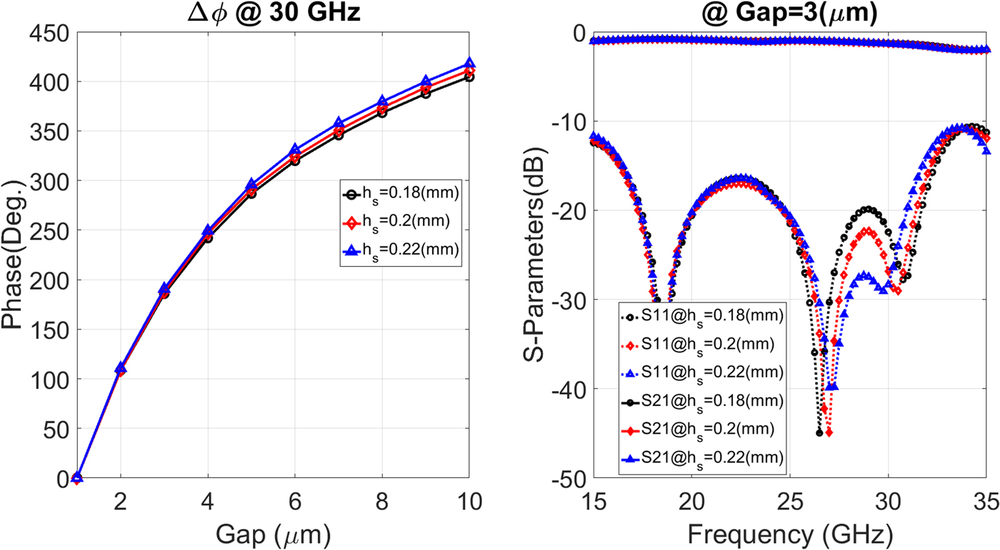
Full wave HFSS simulation was used to perform sensitivity analysis on the proposed phase shifter, which is shown in Fig. 3. A ±5% variation of the dielectric permittivity of the BLT slab demonstrates at 30 GHz ±3.2% variation of the maximum achievable phase variation. Moreover, the proposed phase shifter shows ±1.8% insertion loss variation and ±1.5% frequency shift of return loss. Figure 4 illustrates the effect of the dielectric permittivity variation of the BLT slab on the phase and S-parameters.
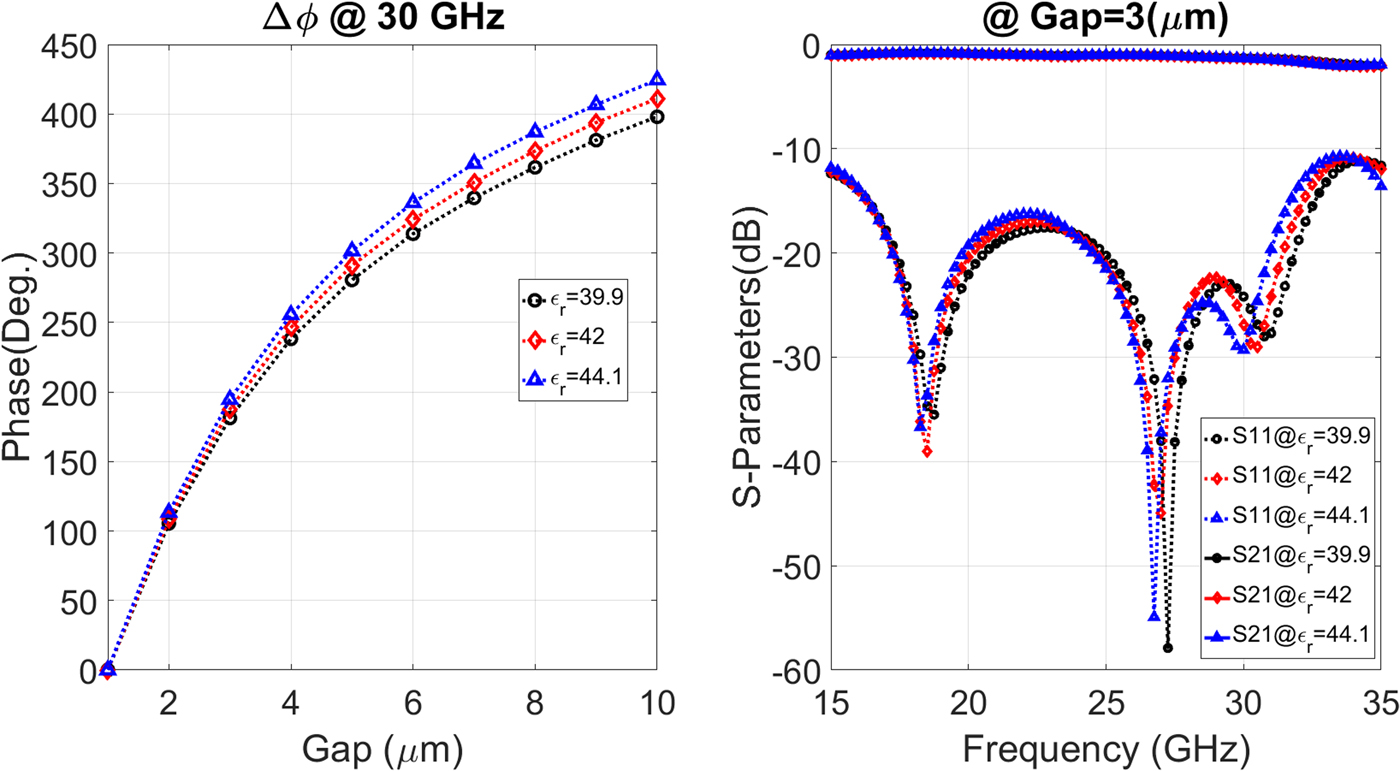
Fig. 4. The effect of the dielectric permittivity variation of the BLT slab on the phase and S-parameters.
Similarly, ±10% variation of the BLT slab thickness demonstrates at 30 GHz ±1.6% variation of the maximum achievable phase variation and ±2.7% insertion loss variation. Figure 5 depicts the effect of the BLT slab thickness variation on the phase and S-parameters.

Fig. 5. The effect of the BLT slab thickness variation on the phase and S-parameters.
Furthermore, misalignment between the BLT slab and the GCPW line shows the most critical case among other variations. A ±100 µm (~±5%) misalignment of the BLT slab in both X and Y leads to 13% increase in the insertion loss of the proposed phase shifter at 30 GHz with the small deterioration of the return loss. However, the maximum achievable phase shift is reduced only by 0.25%. Figure 6 shows the phase shifter performance with misalignment effect on both phase and S-parameters.
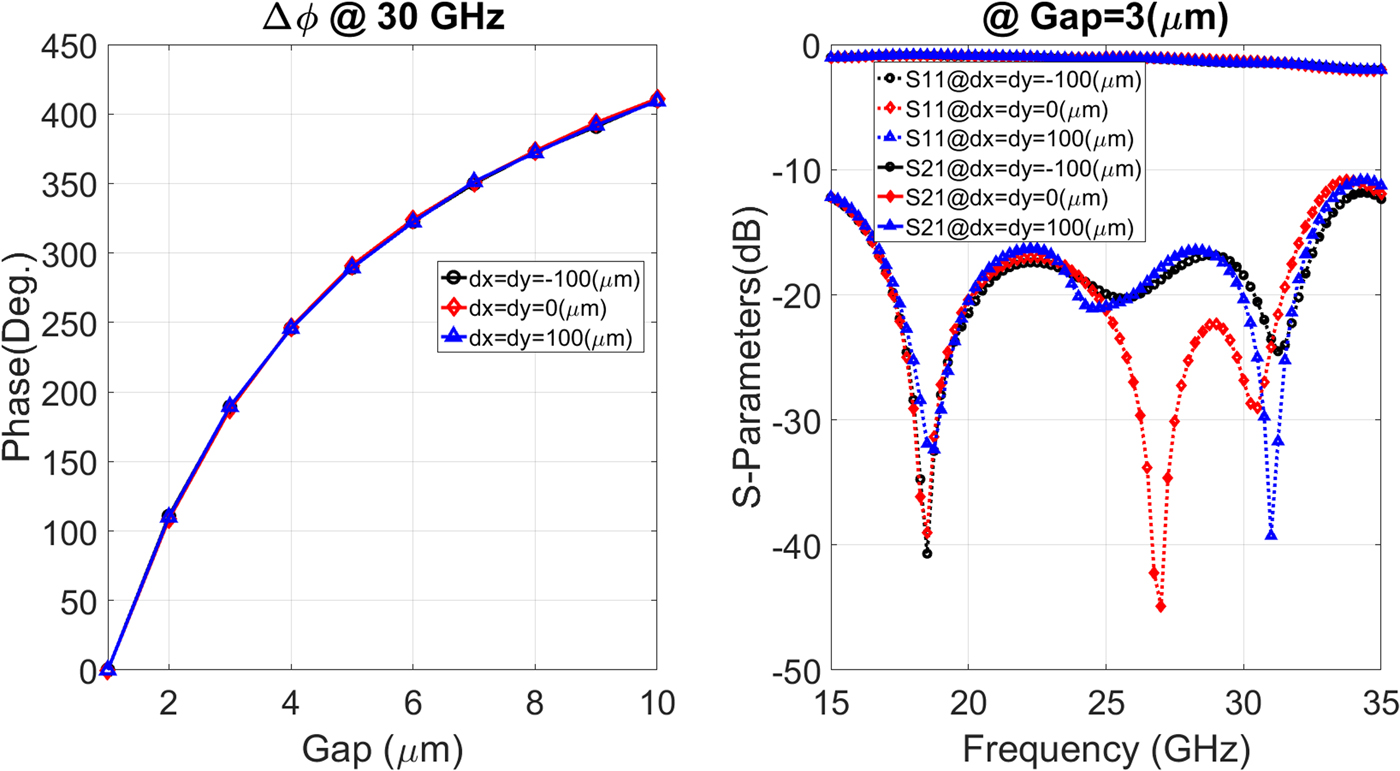
Fig. 6. The phase shifter performance with misalignment effect on both phase and S-parameters.
PET tolerance variation is directly affecting the air gap range that leads to the accuracy of the phase shifter state. The surface roughness issue is another important factor that limits the operation of the proposed phase shifter. However, the accurate model of the surface of the GCPW line and the BLT slab is not available to perform sensitivity analysis due to the surface roughness.
Based on the sensitivity analysis, the proposed phase shifter demonstrates low sensitivity to the fabrication and material tolerance. The insertion loss is highly affected by the misalignment of the BLT slab. On the other hand, phase accuracy is limited by the accuracy and repeatability of the actuation system.
III. FABRICATION PROCESS AND MEASUREMENTS SETUP
A) Fabrication process
The fabrication and measurements are performed at the Centre for Intelligent Antenna and Radio Systems (CIARS), University of Waterloo, Canada. This phase shifter is analyzed at two frequency bands. The GCPW line is fabricated using an LPKF laser machine and the sides are coated with a copper to avoid parallel plate modes. Laser machining is a fast, low-cost, chemical-free, and mask-free process that offers a very precise fabrication capability with the accuracy better than 2 µm. Since the laser fabrication is a non-contact process, the surface of the GCPW line is not damaged or scratched in this fabrication process. The smooth surface is crucial for the proposed phase shifting mechanism as depicted in Fig. 7(a). The power and the movement speed of the laser beam are adjusted to etch the cladding copper completely while providing vertical walls for the traces. In addition to the GCPW line, the laser machine is also used to make high-precision cuts on the ceramic dielectric slab. Since the amount of the phase shift depends on the gap between the ceramic slab and the GCPW line, the surface roughness of both the ceramic and the GCPW lines has to be minimized. In particular, the first few microns of the spacing exhibit the largest phase variation with respect to gap height.

Fig. 7. The fabricated GCPW line and the system fixture. (a) Microscopic image of the fabricated GCPW line, (b) phase shifter assembly with aluminum fixture and PET.
A potentially low-cost and compact PET (AE0203D08F form NEC Cooperation) is used to precisely change the air gap height between the GCPW line and the dielectric slab. This transducer generates 0–9.1 µm continuous displacement by applying 0–150 V DC voltage to its poles. This amount of displacement is sufficient for the proposed phase shifter to achieve more than 360° phase shift variation at 30 GHz. The PET is capable of moving lighter loads at frequencies of more than 10 kHz. In the proposed phase shifter, the PET can reach its nominal displacement within 30 µs. An aluminum fixture is designed to hold the phase shifter substrate and to support the PET. The proposed phase shifter prototype structure including the aluminum fixture is demonstrated in Fig. 7(b).
B) Measurements setup
The measuring setup is shown in Fig. 8, which consists of a 50 GHz PNA-X from Keysight (Agilent), an aluminum fixture to support the GCPW substrate and the PET, a DC power supply from Keysight, and probes with 500 µm pitch. The assembly procedure is as follows. First, the transducer is attached to the fixture arm and the height of the arm is adjusted through the adjusting screw to give the minimum gap for the GCPW substrate and the ceramic dielectric. In the second step, the GCPW substrate is fixed to the base of the fixture and centered underneath the PET. Then, a 100 V DC is applied to the PET to expand the transducer to its recommended maximum length, and finally the ceramic dielectric slab is inserted between the PET and the phase shifter substrate and an adhesive material is used to fix the slab to the PET. Despite all the misalignments, the surface roughness of the GCPW substrate, and manual assembly, the measurement results are in good agreements with those of the simulations. A comparison between the measurements and the theoretical results is presented in the Results section. Then a comparison between the proposed work and alternative continuous, passive phase shifting technologies is also presented.

Fig. 8. Measurement setup.
IV. RESULTS
A) Simulation and measurements results
Extensive full-wave simulations are performed by using HFSS in order to optimize the dimensions of the GCPW line and the dielectric slab. The optimal design is fabricated and tested at room ambient temperature. The measured S-parameters of the phase shifter over the downlink band when 35 V was applied to the PET are presented in Fig. 9(a). The measurement shows a reflection coefficient <−20 dB with insertion loss <0.66 dB over the frequency band. A good agreement between the experimental results and simulation results is observed. Similarly, Fig. 9(b) shows a comparison between the measurements and simulations over the uplink band. The phase shifter exhibits a reflection coefficient <−13 dB with an average insertion loss <2.38 dB over the uplink frequency band. There are some discrepancies between the simulation and measurements are observed, which is mainly due to the slab misalignment to the GCPW line. However, the measurements still match the simulation trends and are sufficiently accurate.

Fig. 9. A comparison of the simulated and measured S-parameters of the phase shifter with control voltage 35 V. (a) Insertion and return loss measured and simulated results @ downlink band. (b) Insertion and return loss measured and simulation results @ uplink band.
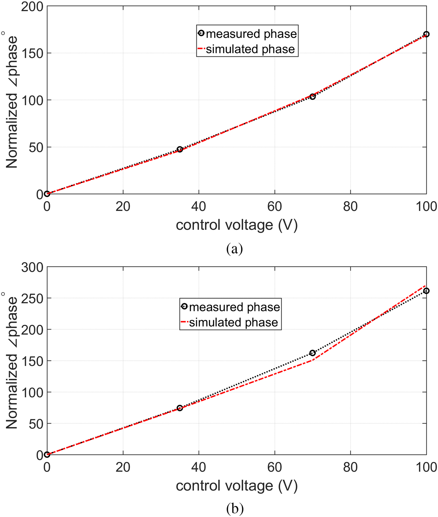
Figures 10(a) and 10(b) show the normalized phase shift variation (with respect to zero applied voltage) versus control voltage at 20 and 30 GHz, respectively. A good agreement between the simulation and measurements is observed over the whole range of the control voltage variation except small discrepancies at few points, which are mainly due to the fact that in the simulations, the control voltage is represented by its equivalent actuation displacement based on the datasheet of the PET besides the misalignment between the BLT slab and the line in the experiment. The proposed phase shifter shows that a 170° phase variation is at 20 GHz and 270.5° at 30 GHz. The realized phase variation is limited in this experiment due to surface roughness of the ceramic slab and PCB substrate, and limited actuation displacement ~0–7 µm when the applied voltage varies between 0 and 100 V. Accordingly, a better surface finish is required; also a larger actuation displacement PET is needed to achieve the 2π phase variation.

Fig. 10. Comparison of the phase delay versus control voltage measurement and simulation (a) phase delay at 20 GHz, (b) phase delay at 30 GHz.
Figure 11 shows the measured S-parameters of the phase shifter over the downlink band for different actuation voltages. A reflection coefficient <−17 dB with low average insertion loss ~0.53 dB and low average insertion loss variation ±0.22 dB is observed, as shown in Fig. 11(a) over the entire phase shift range. Furthermore, the measured average phase shift variation of 170° is achieved, when the control voltage varies between 0 and 100 V at downlink band, as shown in Fig. 11(b) (the phase state at 0 V is considered as a reference).

Fig. 11. Downlink measured results with different control voltages. (a) Insertion and return loss, (b) phase variation.
Similarly, the phase shifter is tested over the uplink frequency band, where it exhibits a good reflection coefficient <−10 dB over the entire phase shift range with average insertion loss ~2.35 dB and the average insertion loss variation is <±0.35 dB over the frequency band, as shown in Fig. 12(a). Additionally, the measured average phase shift variation of 260° is achieved, when the control voltage varies between 0 and 100 V, as shown in Fig. 12(b) (the phase state at 0 V is considered as a reference).

Fig. 12. Uplink measured results with different control voltages. (a) Insertion and return loss, (b) phase variation.
B) Summary of the results
The proposed phase shifter demonstrates a continuous monotonic linear phase–voltage response. It operates over a wide frequency range with acceptable return loss and insertion loss performance over the entire range of the phase shift. The repeatability of the proposed structure has been tested by re-measuring the phase shifter under test with the same voltage settings for different samples repeatedly. This phase shifter can be implemented on any low-cost PCB substrate with almost no impact on its performance. The comparison of the proposed phase shifter with the state-of-the-art phase shifters developed by other technologies is shown in Table 2.
Table 2. Comparison of state-of-the-art phase shifters.
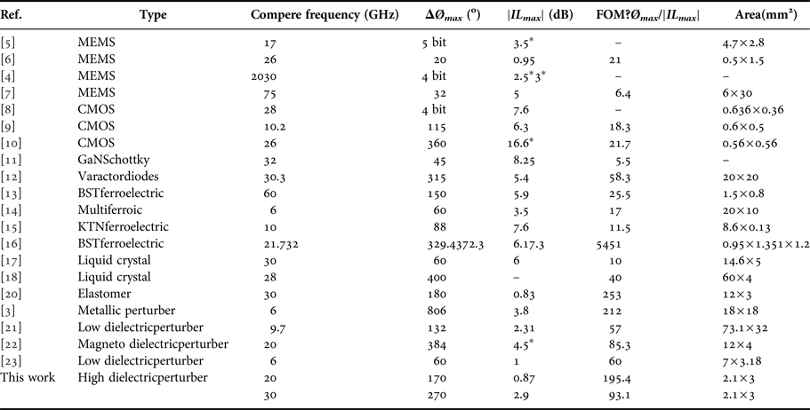
*Estimated from the results
IV. CONCLUSION
In this paper, a high-performance phase shifter structure is proposed and implemented in a low-cost standard two-layer PCB technology. The development of the proposed phase shifter enables the realization of a low-cost mm-wave passive phased array, which is in high demand for numerous emerging mm-wave applications. This paper presents a proof of the concept for a high performance mm-wave phase shifter. The proposed phase shifter shows that high-performance capabilities can be achieved with low-cost PCB technology, but there are some challenges that should be addressed in integrating the current phase shifter prototype in the practical communication systems. The PET size and the driving voltage can be one of the most important challenges for large-scale antenna systems. Misalignment and surface roughness are other important challenges of the proposed phase shifter. A planar low-profile and efficient packaging system based on MEMS and three-dimensional printing technologies are currently under development to overcome the PET challenges and misalignment issues. The results of the new packaged system will be demonstrated in a future paper by the authors. Surface roughness problem can be minimized by either using appropriate surface treatment technology, using low surface roughness copper foil materials or increasing the air gap range. The proposed design concept offers a promising performance over two frequency bands. A higher dielectric constant slab (ε r = 80 or 100) and a PET with more actuation displacement (15 µm) can be used to increase the phase shift variation at both bands within the same footprint. The proposed phase shifter shows a high FOM of 195.4°/dB at 20 GHz and a FOM of 93.1°/dB at 30 GHz, respectively. The main contributions in this work as compared with the work presented in [Reference Abdellatif24, Reference Abdellatif25] are: the proposed phase shifter is developed on a low-cost PCB GCPW meander line, which reduces the fabrication and integration cost significantly; also GCPW is a preferable choice for multilayer phased array antenna as compared with CPW line. In this research, a simple matching technique is presented to overcome the limitation of the previous works. A simple analytical formula is developed to calculate the dielectric permittivity and the length of the BLT slab to obtain the required phase variation at the operating frequency. The proposed phase shifter can be directly integrated into the feeding network, which means no BGA or wire bonding required. Therefore, it can be used in high-power handling feeding networks. Moreover, a wide phase–voltage variation has been experimentally demonstrated in this paper at two different frequency bands.
ACKNOWLEDGEMENTS
This work was supported by the Iraqi Ministry of Higher Education, C-Com Satellite Systems Inc., and the National Science and Engineering Research Council (NSERC) of Canada.
 Hussam Al-Saedi received his M.Sc. degree in Electronic Engineering from The Polytechnic University of Turin, Italy in 2010. He is a Ph.D. candidate in the Electrical and Computer Engineering at the University of Waterloo, Canada, since 2013. His main research interests are phased array antennas, tunable reflectarray antennas, and millimeter passive circuit components. He has authored more than 20 peer-reviewed journal and conference papers. Hussam Al-Saedi serves as a technical reviewer for many journals, such as IEEE Antennas and Propagation Magazine, The Journal of Infrared, Millimeter, and Terahertz Waves, and the International Journal of Antennas and Propagation.
 Wael M. Abdel-Wahab received the Ph.D degree in Electrical and Computer Engineering from the University of Waterloo (UW), Canada in 2011 in microwave and antenna engineering. From 2011 to 2014, he was a Cross-appointed Postdoctoral Fellow with Electrical and Computer Engineering, University of Waterloo and Department of Electrical, Computer and Software Engineering, University of Ontario Institute of Technology, Canada. Currently, he is a Researcher with ERI and a Visiting Scientist at the Centre of Intelligent Antenna and Radio Systems (CIARS) at UW, ON, Canada. His current research interests focus on low-cost emerging technologies for millimeter-wave phased array antenna and multilayer passive circuit components. He has authored many research papers in highly cited journals and conferences. Dr. Abdel-Wahab serves as a technical reviewer for many journals, such as IEEE Transaction on Antenna and Propagations (IEEE TAP), IEEE Antenna and Wireless Propagation Letters (IEEE AWPL), IEEE Microwave and Wireless Components Letters (IEEE MWCL).
 Suren Gigoyan received the M.S. degree from the Physics Department, Yerevan State University, Yerevan, Armenia, in 1980, and Ph.D. degree in Electrical Engineering from the Institute of Electrical Engineering, Moscow, Russia, in 1991. From 2005 to 2006, he was a visiting Fulbright scholar at the University of Tennessee. He is currently a Visitor Scientist at the Microwave and Photonics Integrated System Lab, University of Waterloo, Waterloo, ON, Canada. His current research interests are millimeter and THz spectroscopy, sub-millimeter frequency range devices and system design, application of MEMS structures in THz spectroscopy, sensing, cancer, and DNA detection. He has published more than 60 peer-reviewed journal and conference papers.
 Aidin Taeb He received the B.Sc. degree in Electrical Engineering from Tabriz University, Tabriz, Iran, in 2003; the M.Sc. degree in Electromagnetic and Antennas from Amirkabir University of Technology (Tehran Polytechnique), Tehran, Iran, in 2006, and the Ph.D. degree in Electrical and Computer Engineering from the University of Waterloo, Waterloo, ON, Canada, in 2015. Between September 2006 and August 2007, he was with Microwave/Antenna Group, Fanamoj Co., Tehran, Iran. Currently, he is a Postdoctoral Fellow with the Centre for Intelligent Antenna and Radio Systems (CIARS) Group, University of Waterloo. He is currently investigating the new generation of sub-mmWave and terahertz components. His interests include mmWave/THz biosensors, more specifically DNA, and protein sensors. Other areas in which he has worked are design of satellite antennas, mmWave cancer detector, and mmWave/THz silicon on-chip/in-package circuits.
 Safieddin Safavi-Naeini received Ph.D. degrees from the University of Illinois at Urbana–Champaign, Champaign, IL, USA, in 1979, respectively, all in Electrical Engineering. He is currently a Professor in the Department of Electrical and Computer Engineering, University of Waterloo, Waterloo, ON, Canada, and the NSERC/C-COM Industrial Research Chair in Intelligent Radio/Antenna and Novel Electromagnetic Media, where he is also the Director of the Center for Intelligent Antenna and Radio System. He has authored over140 journal papers and 300 conference papers in international conferences. His current research interests include a wide range of applications of electromagnetic devices and systems, including RF/microwave technologies, smart integrated antennas and radio systems. Moreover, his research includes mmW/THz integrated technologies, vehicular communication systems, emerging radio technologies for intelligent transportation systems, nano-EM and photonics, EM in health science and pharmaceutical engineering, wireless communications and sensor systems and networks, new EM materials, bioelectromagnetics, biomedical instruments, and computational methods.