


Introduction
RFIDs have been steadily taking part in many aspects of our lives in various applications. In the past few decades, researchers have shown a noticeable interest in RFID systems. Many systems were presented with their different techniques and aspects. A brief classification for RFID tags in the market in terms of power, communication range and protocol, and data processing is elaborated in Fig. 1 [Reference Finkenzeller1]. RFID tags introduced to the market were categorized according to a different point of views: power, communication range, programmability, and data processing. From the power point of view, the RFID systems are sub-categorized into active [Reference Karmakar, Roy, Preradovic, Vo and Jenvey2], semi-active [Reference Silva, Sousa and Plett3, Reference Preradovic, Karmakar and Balbin4], and passive [Reference Kisic, Dakic, Damnjanovic, Menicanin, Blaz and Zivanov5–Reference Herrojo, Mata-Contreras, Paredes and Martın7]. Moreover, from the communication range point of view, they are sub-categorized into three main categories: close coupled [Reference Herrojo, Mata-Contreras, Paredes and Martın7, Reference Benamara, Grzeskowiak, Diet, Conessa, Lissorgues and Le Bihan8], remote coupled, and long range [Reference Preradovic and Karmakar9, Reference Mukherjee10]. Nowadays, several applications facilitate the use of simple passive RFID tags to limit the cost of the ID tag unit and introduce relatively more complexity to the reader design. Several RFID tag technologies managed to give several appealing inexpensive solutions and sustain the functionality of the given system, such as low-cost, thin, light weighted, and flexible tags. Those mentioned tags show good mechanical and electrical properties. RFID tags being flexible is an advantageous point as they can be stored easily and are preferable for daily use. In order to ensure the sustainability of the flexible substrate for the desired RFID applications, the fabricated tags should be subjected to several movements such as bending, folding, and twisting repeatedly to test their robustness. According to [Reference Hota, Bera and Maiti11–Reference Blaž, Kisić, Žlebič, Marić and Živanov13], the flexible tags showed reversible electrical characteristics during the bending tests. Many passive RFID tags use transmission lines and micro-strip patch antennas, most of which are used for long-range and high-frequency applications [Reference Preradovic and Karmakar9, Reference Mukherjee10]. On the other hand, applications with lower frequencies in the order of 10 MHz are used more for relatively very short-range applications. Hence, ID tag design depends very much on lumped element planar patterns such as spiral inductance and interdigitated capacitances [Reference Benamara, Grzeskowiak, Diet, Conessa, Lissorgues and Le Bihan8]. Most current RFID systems involve a silicon chip that would set a limit on the total achievable system cost. However, there are some applications that may have an extra degree of freedom with a reader complexity which leads to a relatively low-cost for the ID tag unit. Several researchers showed a great interest in RFID systems. In [Reference Huang, Sim, Liang, Liao and Yuan14], a low-profile chip-less RFID tag for wrist band applications is presented; however, it requires tuning of slot parameters during its application to get desired resonant frequency. Moreover, a low-cost chip-less RFID tag based on split-ring resonators is demonstrated in [Reference Jang, Lim, Oh, Moon and Yu15], but it cannot be used in applications that require flexible tags. The paper proposes a system with negligible ID tag unit cost, and also a cost-effective reader. The design of the proposed RFID tag depends mainly on some passive resonant distinct load circuits and via patterns that are traced on a planar flexible printed circuit board (PCB). The PCB is light-weight 0.1 mm thin polyamide substrate along with the 18 µm copper clad for the lumped device traces. With the planar spiral inductance and the interdigitated finger capacitance combination on the tag side, distinguishable signal-level variations were obtained at the detector. On the detector side, in addition to the previously mentioned RF signature verification, an extra module is embedded, which employs an additional optical front-end to detect the reflected light pattern and intensity corresponding to via pattern around black silkscreened focus area. This combination of distinct optical and RF patterns along with the corresponding encryption results in a fully functional system that is low-cost, portable, and suitable for daily use. The paper presents in detail the planar passive resonance device tags and the wireless charging opto-electronic detector sub-system designs with the corresponding measurement results. The rest of this paper is organized as follows: the section “RFID design” elaborates on the RFID tag design, where the design of passive structures will be discussed. The section “Lumped elements calculations” presents the calculation methods for the planar capacitance and inductance. The section “Simulations and measurements versus calculations” shows the simulation results used to verify the previously mentioned calculations and compares them with the measurements. The section “Tag circuits and systems” presents the circuit details of the proposed peak voltage detector and wireless charger combo system, and optical front-end of the detector. The system simulations and measurements are provided in the section “Measurements”. Finally, the section “Conclusion” concludes the main findings of this study.
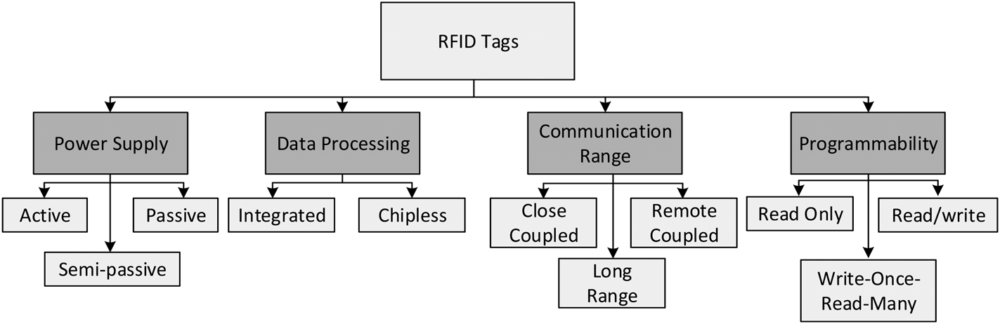
Fig. 1. The classification of RFID tags in the market.
RFID design
As the challenging part of the idea, the proposed RFID tags are chip-less and use very simple planar circuit elements: inductance and capacitance utilizing only copper traces of 18 µm thickness on a flexible substrate. The design is implemented on a single-layer thin flexible PCB (Kapton), which has a low relative dielectric of 3.4 compared to the normal FR-4 dielectric of 4.7. This section introduces the design of two prototype RFID tags with a target size of 69 mm × 159 mm suitable for containing the largest lumped element geometries desired. The first tag has a circular spiral inductance that is equivalent to 556 nH. The coil is formed of three turns with a copper trace width of 0.2 mm, a gap of 0.2 mm as well, and an external diameter of total 25.7 mm, as shown in Fig. 2(a). The second tag has a larger rectangular spiral inductance of 26 µH along with an interdigitated finger capacitance providing an equivalent capacitance of 296 pF. The rectangular spiral inductance is designed with two different trace thicknesses of 0.2 and 0.8 mm to have the best area to inductance ratio, a gap of 0.2 mm, an outer width of 37.7 mm, and an outer length of 62.6 mm. The 45-degree tilted edges ensure robustness for the coil toward any damage as 90-degree transition may suffer from breakdown or failure during active use. The interdigitated finger capacitance is composed of 182 fingers. Each finger is of 65.5 mm length, with a copper trace width of 0.4 mm and a gap of 0.2 mm, which are designed to get a large capacitance to area ratio. This particular tag design is shown in Fig. 2(b). In the middle of tag A, a pattern of four holes is added for the light reflection detection. As for tag B, a pattern of two holes is inserted for the validation of the two detection methods on these limited number of prototypes.

Fig. 2. The design of the two proposed RFID tags: (a) Tag A: the first tag with circular spiral inductance. (b) Tag B: the second tag with the chamfered rectangular inductance and interdigitated finger capacitance. (c) Cross-section of tag B defining the layers.
Lumped elements calculations
Since designing reliably distinguishable RFID tags with only lumped element traces has been the main target of this study, it is necessary to have a reliable approximate value for the first cut lumped elements necessary for the tag design. Many would consider that the advanced 3D EM simulation tools were a good choice for extracting these values, but they might consume a significant amount of simulation time, processing power, and may easily result in inaccurate results when the geometries of interest come to be sophisticated and large [Reference Sheeparamatti, Hanasi, Aibbigeri and Meti16]. In order to speed up the design of the RFID tags, this section elaborates on fast calculation techniques for interdigitated finger capacitance and the various geometries of a spiral inductance to obtain a close estimate of resonances on the target tag structures.
Capacitance calculations
In order to go through calculations, there is a need to define the interdigitated finger capacitance's geometry and related parameters. Figure 3 illustrates an interdigitated finger capacitance of n = 5 where n is the number of fingers, G is the gap between two fingers, L is the common length between two fingers, and W is the width of a single finger capacitance. The calculation method to be mentioned is only valid for capacitance with a finger thickness relatively small compared to its width. The capacitance value is dependent on the gap to metal ratio, which is defined as the metallization ratio represented by equation (1):
 $$\eta = \displaystyle{W \over {W + G}}.$$
Fig. 3. Five fingers interdigitated finger capacitance.
This type of capacitance is excited by the differential voltage. The top comb with positive voltage V + and the bottom comb with negative voltage V −. Consequently, the middle distance between two successive fingers would be virtually grounded and the capacitance will be defined as given in Fig. 4(a), where the capacitance is divided into two categories, interior capacitance noted as C I and exterior capacitance noted as C E. This structures' equivalent model is illustrated in Fig. 4(b). From Fig. 4(b), the overall capacitance value C T can be obtained in terms of the internal and external capacitance, C I and C Erespectively, as shown in equation (2):
 $$C_T = \lpar {N-3} \rpar \times \displaystyle{{C_I} \over 2} + \displaystyle{{2\lpar {C_I \times C_E} \rpar } \over {C_I + C_E}}, \quad N \gt 3.$$
Fig. 4. Capacitance model: (a) Capacitance between fingers on substrate. (b) Equivalent circuit model.
According to [Reference Igreja and Dias17, Reference Khan and Reddy18],C I and C E are defined by equations (3) and (4) respectively, and the complete elliptic integral of K(k), K(k ′) is necessary, where k and k ′ are the modulus and the complimentary modulus, respectively:
 $$C_I = {\rm \varepsilon} _0\lpar {\varepsilon_s + 1} \rpar L\displaystyle{{K\lpar {k_{I\infty}} \rpar } \over {K\lpar {k_{I\infty}^{\prime}} \rpar }},$$
 $$C_E = {\rm \varepsilon} _0\lpar {\varepsilon_s + 1} \rpar L\displaystyle{{K\lpar {k_{E\infty}} \rpar } \over {K\lpar {k_{E\infty}^{\prime}} \rpar }},$$
where ɛo is the absolute dielectric constant of air, and ɛs is the relative dielectric of the substrate. The modulus and complementary modulus of the internal capacitance differ from one case to another according to the height of the dielectric and how many dielectric materials the design has. As for this work, only the substrate is available and the upper dielectric is an infinite layer of air [Reference Igreja and Dias17]. Hence the values of k and K ′ will be defined for this case by equations (5) and (6):
 $$k_{E\infty \;} = \displaystyle{{2\sqrt \eta} \over {1 + \eta}} \;, \quad k_{E\infty} ^{\prime} = \sqrt {1-k_{E\infty}}, $$
 $$k_{I\infty \;} = \sin \left( {\displaystyle{\pi \over 2}\eta} \right),\; \quad k_{I\infty} ^{\prime} = \sqrt {1-k_{I\infty}}. $$
As mentioned, it is necessary to solve the complete elliptic integral of the first kind which is defined by equation (7):
 $$K\lpar k \rpar = \int_0^1 {\displaystyle{{dt} \over {\lpar {1-t^2} \rpar \lpar {1-{\lpar {kt} \rpar }^2} \rpar }}}. $$
Due to the complexity of solving this integral, a MATLAB code was developed to ease the evaluation of the integral and obtaining the value of total capacitance.
Inductance calculations
The initial tag prototypes in this work have considered two extreme geometries for spiral inductances. One of them is a regular circular spiral inductance with a limited number of turns as shown in Fig. 5(a), and the other one is a rectangular shape with dense turn ratio as shown in Fig. 5(b). Two different wire thicknesses were utilized along the vertical and horizontal tracks, utilizing the given area for maximum inductance value. As regards to the circular coil, its inductance can be simply calculated according to [Reference Mohan, del Mar Hershenson, Boyd and Lee19]; depending on the current sheet approximation, its inductance is defined by equation (10), where μ is the permeability, n is the number of turns, d avg is the average distance between the outer and inner diameter, ρ is the fill factor, and C I are the coefficients dependent on the geometry as given in Table 1. This method takes into consideration the symmetry of the spiral geometry and hence offers an approximation for the sides of the spirals by symmetrical current sheets of equivalent current densities. Moreover, as elaborated in [Reference Mohan, del Mar Hershenson, Boyd and Lee19], the total inductance of a square structure is the sum of four identical values obtained by the current sheets, since the four sides are identical.
 $$d_{{\rm avg}} = \displaystyle{{d_{{\rm out}} + d_{{\rm in}}} \over 2},$$
 $$\rho = \displaystyle{{d_{{\rm out}}-d_{{\rm in}}} \over {d_{{\rm out}} + d_{{\rm in}}}},$$
 $$L_{{\rm circ}} = \displaystyle{{\mu n^2d_{{\rm avg}}c_1} \over 2}\left( {\ln \left( {\displaystyle{{c_2} \over \rho}} \right) + c_3\rho + c_4\rho^2} \right).$$
Fig. 5. Spiral inductance: (a) Circular spiral inductance. (b) Rectangular spiral inductance.
Table 1. Coefficients for current sheet expression

Therefore, using this information, an assumption can be made that one side of the given rectangular coil inductance can be represented by equation (11), with two identical values for the length of the rectangular coil and two others for the width. Given all the equations needed to get the total inductance of this unique coil.
 $$L_{{\rm side}} = \displaystyle{{\mu n^2d_{{\rm av}{\rm g}_{{\rm side}}}c_1} \over 8}\left( {\ln \left( {\displaystyle{{c_2} \over \rho}} \right) + c_3\rho + c_4\rho^2} \right),$$
 $$L_{{\rm rec}{\rm t}_{{\rm total}}} = 2\; \lpar {L_{{\rm side} = W} + L_{{\rm side} = L}} \rpar.$$
Simulations and measurements versus calculations
In order to prove that the driven calculation methods are sufficient, simulations and measurements are needed to verify the equations’ veracity.
Capacitance simulations and measurements versus calculations
As stated in [Reference Sheeparamatti, Hanasi, Aibbigeri and Meti16], the simulation tools cannot get a reliable value of capacitance when the number of fingers exceeds 50. Consequently, it is compulsory to verify the calculations and simulations for a smaller number of fingers. Using ANSYS Maxwell software, the equivalent capacitance value was acquired for several capacitances of a different number of fingers and compared with calculations for a capacitance of a finger length 65.5 mm, a gap of 0.2 mm, and a finger width of 0.4 mm. Figure 6 plots the comparison of both simulated and calculated values of capacitance for a number of fingers ranging from 4 to 32. Since this simple calculation method more or less converges with the simulation results, it is more appropriate to build a test prototype with a capacitance value of 183 fingers, and compare the results with the measured values after fabrication, as shown in Table 2. The error between the calculated and measured value was around 1%.

Fig. 6. Simulated and calculated capacitance versus number of fingers.
Table 2. Calculated versus measured capacitance values

Inductance simulations and measurements
Verifying the inductance value was a relatively easier task compared to the capacitance. Table 3 elaborates the results of the calculated, simulated, and measured values of both proposed circular and rectangular spiral inductances. Inductor simulations were as well conducted with the help of ANSYS Maxwell CAD EM design tool to extract estimate values for those specific geometries. The circular spiral inductance had an outer diameter of 25.7 mm, a wire thickness of 0.2 mm, a gap of 0.2 mm, and three number of turns, while the rectangular spiral inductance was designed for an outer width and length of 37.7 and 62.6 mm, respectively, two thicknesses of 0.2 and 0.4 mm, 22 turns with a gap of 0.2 mm. Taking into consideration the parameters of the Kapton substrate of a relative dielectric of 3.4 and a loss tangent of 0.0036.
Table 3. Calculated, simulated, and measured inductance values for both proposed spiral inductors

Tag circuits and systems
The circuit diagram of the proposed low-cost RFID system including the reader and charger is shown in Fig. 7. In addition to accurate planar thin-film passive circuit element design methodologies described in previous sections, associated peripheral detector and charger circuits are also discussed in detail in this section. The reader design involves a single Bluetooth Low-Energy (BLE) IC as a full controller and communication device. Simple fully differential 3 MHz signals are applied to a series network of a 200 Ω total resistor and a PCB-trace detector receive coil L rx of about 20 turns. The 100 Ω insulation resistors serve two purposes. First, they limit the current to be drawn from the BLE GPIO drivers, which is not a significant amount for the low-power IC and hence allow an optimal voltage swing. Second, they form an intermediate variable impedance measurement taps for the RX detector coil to allow sensing of the variable load resulting from various planar tag inductive resonance circuits inserted. In order to enhance the effective coupling between the reader and the tag, center gap for the reader coil is aligned with the center gap of the tag which is arranged to be matching by design. In order to minimize the user read out errors, the notes are inserted into a guided sandwiched upper and lower double-plated PCB coil structure with 1.5 mm gap, which effectively eliminates the gap errors in the vertical direction. In the direction of insertion, the notes progress stops at the sidewall removing these variations, as well. The last variation, which is responsible for the largest reading error source, relates to the shifts toward the sides in the horizontal plane. In order to minimize this shift error, the center gap of the reader coil is made slightly larger to accommodate 7–10 mm shifts. Even if a larger shift were to be exerted by the user, the optical detector determines this case easily and asks the user to insert the note properly. The only thing that varies on the tag side is the number of turns as well as the capacitive load resulting in a distinct level of attenuation in the detected signal. In order to keep stable alignment with repeatable and distinguishable load detection levels; the thin film tags are expected to be inserted between two fixed-gap PCBs. The sense path to this differential coil is a differential to single-ended conversion transformer TR1 with 1:2 turn-ratio, which is chosen to both amplify the detected load difference voltage into a high impedance load of peak detector NMOS gate and also to achieve proper isolation into the DC bias levels set in the envelope peak detector. The output of this peak detector is fed into the analog to digital converter (ADC) of the BLE for the final decision. The receiver coil is not only used to detect the unique tag RFIDs but it is also used to charge the unit wirelessly. Since the design is a fully sealed waterproof unit, the embedded 3.7 V Lithium-Polymer battery needs to be charged wirelessly. A standard Q i charger is able to charge the unit with a 175 kHz tone, even without a secondary side resonant tuning capacitor. It should be noted that the coil itself had to be kept wideband without any resonance not to impact the regular sensing operation of a wide frequency range of various tag coils, while simultaneously charging the battery with a safe margin. Two-way differential Zener clamp circuitry is used to protect the BLE chip, in case a large Q i charging field is encountered. The Zener clamp voltage level was set around 5.9 V which allows large enough headroom for the Lithium battery charger circuit after the rectifier diode drops and does not push the devices into breakdown regions if the charging field happens to be excess in strength (Fig. 8).
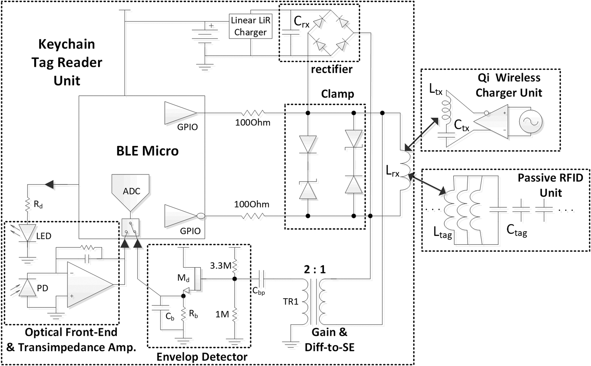
Fig. 7. RFID system circuits diagram along with the reader and the charger circuits.

Fig. 8. The proposed system in detection mode when the tag is inserted.
The last circuit in the detector system is an optical front-end which is responsible for sensing the light intensity variation that results from the various minimum size via patterns engraved in the center of the coil in the tag. On the corresponding region of the bottom PCB of the two-layer detection circuit is a no solder mask reflector metal area that reflects the light that is produced on the top PCB. A photo-diode and light-emitting diode (LED) pair combo device on the back of this top PCB is activated by the controller during the tag readout, detecting the level of light that can go through and reflect back. In the corresponding area of the Kapton film tag, there exists a hole pattern with dark black silkscreen to improve the sensitivity of this low-cost detection mechanism. A small photodiode current is amplified through a trans-impedance amplifier and fed into the ADC for the final level decision in the microcontroller.
Measurements
After elaborating on the functionality of the proposed system circuitry, this section discusses the measurement results of the proposed system. As mentioned before that the system has two identification criterions; one is measuring the change in peak voltage due to the inserted resonant tag load; the other is measuring the equivalent current intensity due to the reflected light intensity between the reader and the tag corresponding to the hole pattern of the proposed via structure. This section will discuss the results of the two detection methods separately.
Voltage difference detection
As illustrated in Fig. 9 of the measurement setup, the reader is fed by a 3 MHz square wave of 4-Volt peak-to-peak differential signal. The screenshot demonstrates the output on the oscilloscope for the given three cases, no tag inserted, tag A case, and tag B case; two distinct prototypes that were manufactured for test purposes.

Fig. 9. Voltage difference measurements setup for tag B.
There was 500 mV of a received signal-level difference between the tags as shown in Fig. 10, where the signal level drops from 3.3 to 3 V in the case of tag A as a load and it drops to 2.5 V in the case of tag B, with a dynamic range of 500 mV without even amplification. Hence, the design provides flexibility to design eight different structures to correspond to eight different tag designs with safe margins. From this specific RF-based detection mechanism, 3-bit extraction is used to identify the uniqueness of each particular tag, with a Least Significant Bit (LSB) of 65 mV which could be easily differentiated using the ADC in the controller.

Fig. 10. Voltage levels measured after insertion of the proposed tag loads.
Current intensity detection measurements
This particular detection mechanism measures the photo-diode current level corresponding to the reflected light intensity resulting from the hole pattern implemented on the tags. In Fig. 11, trans-impedance amplifier output measurements corresponding to a number of holes in the patterns of tag A and tag B are illustrated by the black solid line showing a quiet linear behavior with the dashed interpolation line. It is possible to extrapolate these initial test results with a limited number of holes from the mentioned two test tags to conclude with up to 32 holes for safe detection dynamic range. This provides an additional 5-bit variety in a number of distinct tags that can be constructed.

Fig. 11. Trans-impedance Amp. output versus number of holes.
Conclusion
This paper described a low-cost and robust low-power RFID tag and a reader technology for many daily activities such as tickets, gaming, temporary activity tags, etc. The tags could be produced in a standard single-layer copper-clad flexible substrate production technology without any component or assembly requirement. The tags are just planar printed circuits and hole patterns, while the wireless charging reader is designed as simple as two sandwich layers of two-layer each FR-4 PCBs housing all the reading circuits and PCB trace coils. A water-proof and stress-proof feature of the proposed design allows it to be used in the form of a keychain that can be carried along everywhere by individual users. Table 4 illustrates the differences between the proposed work and other published works.
Table 4. Comparison with published works

Acknowledgements
The authors would like to thank Mert Karaca of Microelectronics Labs at Özyeğin University for his help in accurate impedance measurement and characterizations of the designed TAG units.
 Salma El-Sawy was born in Egypt, received her B.Sc. degree from Ainshams University (Egypt) Faculty of Engineering, Electronics and Communication Department in 2013. In 2014, she joined CST Middle east as a verification and research engineer. She moved to Istanbul and joined Özyegin University electric and electronic department in 2017 to pursue her M.Sc. degree. Her main interests include circuit designs, analog, and mixed signals integrated circuits design.
 Wasim Nawaz received his undergraduate degree in Electrical Engineering from Pakistan's high ranking engineering institute, Pakistan Institute of Engineering and Applied Sciences (PIEAS) in 2013. After that, he worked in a research organization for more than 3 years. His main area of research is RF front end including antennas and passive microwave circuits. Except for this research, his work is already presented and published in IEEE International conferences including ICASE (2015), ICS (2016), and ComTECH (2017). Apart from R&D in the field of Antennas and Microwave, he also has in-depth knowledge and experience on testing antenna systems in anechoic chamber and near-field scanning facility. Currently he is a graduate student of the Department of Electrical and Electronics Engineering at Özyeğin University and working as an RF Front End Engineer at Analog and RF Labs under the supervision of Dr. Ahmet Tekin.
 Mohamed Osama was born in Cairo, Egypt in 1992. He received the B.Sc. degree in Electrical and Communication Engineering from Cairo University, in 2014. In 2016, he started his M.Sc. degree at Ozyegin University. In 2014, he received the second best graduation project prize sponsored by Mentor Graphics in Egypt. In 2016, he received full scholarship including housing from Ozyegin University where he is currently pursuing his M.Sc. degree. From 2014 to present, he is working as a firmware developer at WaveWorks Inc. His research interests include RF, analog circuit design, power amplifiers, and biomedical electronic devices.
 Ahmet Tekin has received his EE Ph.D. degree from the University of California Santa Cruz, CA, USA; EE MS degree from North Carolina A&T State University, Greensboro, NC, USA; and EE BS degree from Bogazici University, Istanbul, Turkey in 2008, 2004, and 2002, respectively. In addition to academic research in microelectronics, he worked for multiple innovative semiconductor design companies such as Multigig, Inc., Newport Media, Aydeekay LLC, Broadcom corp., Semtech Corp., Nuvoton Technology Corp., Qualcomm and Waveworks Inc., leading designs for communications, consumer, and medical markets. His main focus area is analog/RF/mixed-signal integrated circuit design for communication and biomedical applications. He is currently the head of Analog&RF Labs at Özyeğin University and serves in the board of directors of Waveworks Inc., Mission Viejo, CA, USA.


