I. INTRODUCTION
Due to the advantages of low profile, circularly polarized (CP) microstrip antennas are widely developed for satellite communications and navigations [Reference Prajapati, Murthy, Patnaik and Kartikeyan1–Reference Nasimuddin, Qin and Chen4]. Up to the present, many studies have been made on the miniaturization of CP microstrip antennas. The miniaturization methods mainly content the following. One is to utilize high-permittivity substrates. This method often brings a simple structure of the antenna but a narrow bandwidth and a low radiation efficiency. One is to use meander or fractal structures to increase the current paths in a limited area, but it also leads to a narrow band [Reference Cai, Wang, Zhang and Shi5, Reference Farswan, Gautam, Kanaujia and Rambabu6]. The other is to adopt shorting and coupling structure to miniaturize the radiation patches, which usually brings a flexible design but a complex structure [Reference Liu, Shen, Liu and Wu7–Reference Sun, Zheng and Liu9]. In these flexible designs, lossy feed networks are usually utilized to excite CP operation, and the bandwidth of the antenna will be broadened due to the participation of isolation resistors or absorbing loads. Adversely, the radiation efficiency and gain will drop obviously [Reference Sun, Zheng and Liu9–Reference Sun, Zheng, Zhang and Liu11]. From the above status, it is known the studies on the compact CP antenna with high efficiency and satisfactory bandwidth are always desired.
In this paper, a low-cost and compact three-dimensional (3D) CP microstrip antenna is proposed. The antenna is designed on the surface of a low-profile cylinder, which is formed by three printed circuit boards (PCBs). This structure makes the antenna light and solid. Because of adopting a radiation patch with a crossed slot and triangular feed patches, the antenna acquires wideband properties with a miniaturized structure. Meanwhile, due to using a low-loss feed network, a high radiation efficiency is also obtained in the operating band.
The contributions of the work can be summarized as follows: (1) a novel compact CP microstrip antenna, which has a high efficiency and wide beamwidths, is proposed; (2) a novel integrated structure of the radiation patch and the feed patch are proposed, which can increase the bandwidths of the CP antenna with a miniaturized structure; (3) a low-cost method of constructing 3D antennas is adopted. In the following sections, the configuration of the antenna are presented in Section II. In Section III, its operation principle is discussed. The experimental results and discussions are given in Section IV. Finally, the conclusion is summarized.
II. CONFIGURATION OF THE PROPOSED ANTENNA
A) Configuration of the antenna
Figure 1 shows the full view of the proposed antenna whose appearance is a low-profile cylinder. Figure 2(a) shows the exploded view of the antenna. From top to bottom, the antenna consists of three components: a radiation PCB, a feed cylinder and a network PCB. These three components form an integrated and closed structure by themselves, so the antenna is both light and solid. Figure 2(b) shows the radiation PCB, which is based on the 1 mm-thick FR4 substrate with a relative permittivity of 4.4 and a loss tangent of 0.02. A circular radiation patch cut by a crossed slot is etched on the upper surface of the radiation PCB. It can also be considered the crossed slot divides the circular patch into four isolate radiation sectors. This structure can make an effect on miniaturizing the antenna. The diameter of the radiation PCB and the width of the crossed slot are labeled as D p and W s , respectively. For connecting with the feed cylinder, four melding slots are reserved symmetrically on the edge of the radiation PCB. The width of the slot is 1 mm. The feed cylinder is rolled into with a 0.15 mm-thick FR4 sheet, which has the same material as the radiation PCB does. The plane structure of the sheet is shown in Fig. 2(c). Four triangular feed patches are etched uniformly on the sheet, and two holes, which are used for locating and mounting when rolling the sheet, are reserved at both ends of the sheet. In the enlarged local view, it can be seen the top edge of the triangular feed patch has weld slices, which are used to insert the weld slots on the radiation PCB and soldered at the slots. The lower corner of the triangular feed patch is the exciting point, which connects with the output of the feed network. At a distance P s from the exciting point is placed a shorting stub, which is used to adjust the impedance matching of the antenna. At the ends of the exciting point and the shorting stub are also reserved weld slices to insert the weld holes on the network PCB.

Fig. 1. Full view of the proposed antenna.
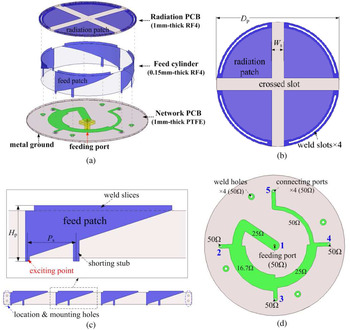
Fig. 2. Configuration of the proposed antenna. (a) Exploded view. (b) Radiation PCB. (c) Plane structure of the feed cylinder. (d) Network PCB.
Under the condition of ideal excitations, i.e. four exciting points with equal amplitude and 90°-difference phase, the radiation PCB and the feed cylinder form the basic radiation structure (Fig. 4(a)), which mainly decides the properties of the proposed CP antenna. In Section III, the special analyses and discussions on the basic radiation structure will be presented.
B) Feed network
For a practical CP excitation, a feed network should be adopted. Usually, a parallel feed network, such as power divider and coupler, can provide wideband properties for a CP antenna, but it occupies a larger area and lead to large loss, which comes from the usage of isolation resistors or absorbing loads [Reference Sun, Zheng and Liu9–Reference Sun, Zheng, Zhang and Liu11]. Although a series feed network provides narrower bandwidths than a parallel feed network does, it has the advantages of low loss and compact layout. In fact, a satisfactory bandwidth may also be obtained if the antenna and the series network are designed carefully, and a high radiation efficiency of the antenna will be acquired.
In our design, a compact series feed line is designed on the network PCB. The network PCB is placed under the feed cylinder, and it adopts a 1 mm-thick polytetrafluoroethylene substrate with a relative permittivity of 3.5 and a loss tangent of 0.002. A series-feed microstrip line is etched on the upper surface of the PCB. The layout of the microstrip line is shown in Fig. 2(d). The feed line is formed by several arcs. One feeding port is located at the center, and four connecting ports are leaded from the arcs successively. The arc length of each segment dominates the 90°-phase difference between two adjacent connecting ports. The characteristic impedance of each segment is determined by the matched impedance and the desired power ratio of these ports. Figure 3(a) shows the design mechanism of the network. When the feeding port and four connecting ports are designed to match with 50 Ω and be equal in power output, the characteristic impedance of each arc microstrip line can be derived from the impedance relationship in Fig. 3(a). From the bottom to the top, the power distribution is divided into three levels, and each level has its own power ratio which is 1:1, 1:2 and 1:3, respectively. According to the power distributions, the characteristic impedance of each line can be calculated in sequence from the bottom. Just one quarter-lambda (λ) impedance transformer line is needed at the feeding port. The performance of the network is evaluated by the EM simulation software – Ansys HFSS (same as the following calculation). Figures 3(b) and 3(c) show the results. The wide bandwidth of 1.0–1.4 GHz for voltage standing wave ratio (VSWR) ≤ 1.5 is obtained. In this band, the amplitude ratio is <0.5 dB, and the phase variation from 90° is <15°.

Fig. 3. Principle and performance of the feed network. (a) Design principle of the network. (b) VSWR and transmission coefficients. (c) Transmission phase.
III. OPERATION PRINCIPLE OF THE ANTENNA
The proposed antenna is composed of the basic radiation structure (Fig. 4(a)) and the feed network. Of these, the performance of the feed network has been given in above section. When matched with 50 Ω loads, the network has a wideband property. For clearly understanding the design method of the antenna, the principle of the basic radiation structure will be discussed through the parameter studies in this section, including its miniaturization, bandwidth and impedance matching. The parameters of the basic radiation structure content: D p = 66 mm (0.264λ), H p = 16 mm (0.064λ), W s = 6 mm, P s = 14 mm, and D g = 90 mm (0.36λ). When one parameter is studied, others are fixed.

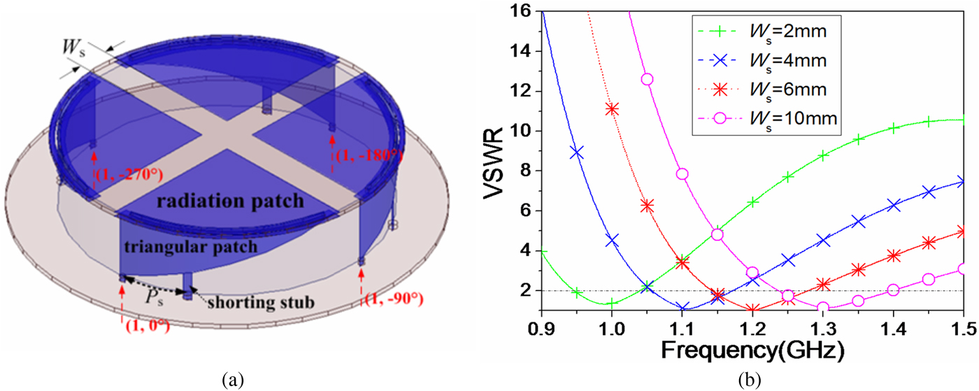
Fig. 4. (a) Basic radiation structure of the triangular-patch type. (b) VSWR with different W s in the case of triangular-patch type.
A) Miniaturization
The height and diameter of the radiation patch are 16 mm (0.064λ) and 66 mm (0.264λ), and such small dimensions come from the effect of the crossed slot. Figure 4(b) shows the variations of the operating band with different width of the slot. As the width increases, the operating band shifts from lower band to upper band. When W s = 2 mm, the center frequency of the band is 1 GHz. Here, the corresponding electrical dimension is just 0.22λ × 0.053λ, so a more compact structure can be acquired. When W s increases to 10 mm, the center frequency moves to 1.3 GHz and the bandwidth is also broadened. Therefore, a suitable width of the slot should be decided by the dimensional limit of the antenna and the desired bandwidth.
B) Bandwidth
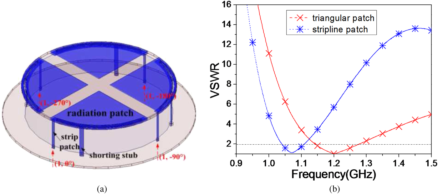
In CP microstrip antennas, strip patches or pins are usually used as feed structures [Reference Liu, Shen, Liu and Wu7–Reference Chen, Yang, Zhao and Fu12]. In our design, the structures of the triangular feed patches are proposed to increase the bandwidth. Here, the comparison of the bandwidth is given between the types of the triangular feed patch and the strip feed patch. Figure 5(a) shows the structure of the strip-patch type, which has the same dimensions with the triangular-patch type. It is observed the bandwidth of the strip-patch type for VSWR ≤ 2 is 1.04–1.106, the relative bandwidth of only 6.2%, while the triangular-patch type reaches a bandwidth of 10.8%, realizing an increase by 74.2%. Thereby, the proposed basic radiation structure has a wider bandwidth than the traditional structure does. In Section IV, it can be seen the axial ratio (AR) bandwidth (10.1%) of the entire antenna is very close to this bandwidth (10.8%), which implies the CP bandwidth of the antenna is mainly decided by the bandwidth of the basic radiation structure.

Fig. 5. (a) Basic radiation structure of the strip-patch type. (b) VSWR in the cases of triangular-patch type and strip-patch type.
C) Impedance matching
With regard to such a small antenna, it is not easy to be matched with 50 Ω. The shorting stub plays an important role on the impedance matching of the basic radiation structure. The smith chart in Figure 6 shows the effect of the shorting stub on the input impedance normalized to 50 Ω. The dash line is the impedance in the case of no shorting stub. It is observed the resistance is small, and it is about 12 Ω at resonance point. After adding the shorting stub, the impedance is increased obviously and close to 50 Ω. In addition, the reactance of the input impedance can be adjusted effectively by changing the position of the shorting stub. When the P s is reduced, the impedance tends to be inductive. Oppositely, when the P s is increased, the impedance tends to be capacitive. On the other hand, the input impedance is not sensitive to the width of the stub.

Fig. 6. Input impedances with different P s .
IV. RESULTS AND DISCUSSIONS
According to the above structure and principle, a prototype of the proposed antenna is fabricated. The main parameters include: D p = 66 mm (0.264λ), H p = 16 mm (0.064λ), W s = 6 mm, P s = 14 mm, and D g = 90 mm (0.36λ). Figure 7 displays the photo of the prototype. All the three components of the antenna are manufactured by the PCB technology, so the manufacturing accuracy and the consistency can be well guaranteed. It is also very easy to assemble the 3D structure. The feed cylinder is formed firstly by its plane structure, and then inserting the reserved weld slices into the corresponding weld holes of the upper and lower PCBs. When the antenna structure is well-determined and stable, welding the connecting points and slots from both sides of the PCBs. From Fig. 7, it can be seen the antenna has an integrated and compact body after welding. Just because of the above manufacturing and assembling advantages, the performance of the antenna is easy to reach the expected results.

Fig. 7. Prototype of the proposed antenna. (a) Front view. (b) Back view.
The measurements are carried out by a vector network analyzer (Agilent E8363B) and a far-field measurement system in anechoic chamber. VSWRs of the antenna are shown in Fig. 8(a). It is observed the measured curve agrees well with the calculated one. The measured bandwidth for VSWR ≤ 2 covers 1.057–1.332 GHz, a relative bandwidth of 23%. The calculated one covers 1.067–1.326 GHz (21.6%). These wide impedance bandwidths come from the effect of the feed network, which is wideband when the connecting ports are matched well. The reflection coefficients (S 11) are also given in Fig. 8(b) for a clear show in the wide band. Meanwhile, because of no resistors used in the feed network, a similarly wide CP bandwidth is not acquired for the small antenna. Figure 8(c) shows the AR bandwidth of the antenna. The calculated bandwidth is 1.139–1.255 GHz (9.7%), and the measured one for AR ≤ 3 dB is 1.138–1.259 GHz (10.1%). However, a high radiation efficiency of the antenna is obtained due to the low loss of the network and the radiation structure. It can be seen, in the overlap band of VSWR and AR, a radiation efficiency is >95%. There into, the radiation efficiency is defined as the ratio of the antenna radiation energy to the antenna receiving energy. To sum up, it is satisfactory to obtain such a CP bandwidth with such high radiation efficiency.

Fig. 8. Bandwidth of the proposed antenna. (a) VSWR. (b) S 11. (c) AR and radiation efficiency. (d) Gain.
From the gain curve in Fig. 8(d), the gain is beyond 4.5 dBic in the band, and the peak gain reaches 4.8 dBic. It is observed, the AR bandwidth of the antenna is very close to the impedance bandwidth (10.8%) of the above basic radiation structure, which implies a relationship between them. If the impedance bandwidth of the basic radiation structure is broadened, the AR bandwidth of the antenna may be enhanced further.
Figure 9 shows the radiation patterns (RPs) and ARs in the elevation plane of φ = 0°, 45°, and 90° at 1.2 GHz. The measured curves and the calculated ones agree well in the main. It is obtained the 3 dB beamwidths of the co-polarized (RHCP) RPs in three planes are 114.8°, 114.3°, and 114.2°, respectively, while the calculated ones are 114.3° and 114.1°. It is indicated a good symmetry and wide beamwidth of the radiation property. As the faint cross-polarization is easy to be affected by the tolerances of manufacturing and assembling, the measured cross-polarization (LHCP) levels are a little higher than those of the calculated ones around the zenith. As shown in Figs 9(b), 9 (d), and 9 (f), the angle ranges for AR ≤ 3 dB are 137° (−69° to 68°), 132° (−67° to 65°), and 131° (−66° to 65°), respectively, which are coincident with the calculated ones. The results indicate a good circular polarization is acquired in the wide beamwidth.

Fig. 9. RPs and AR RPs of the proposed antenna at 1.2 GHz. Solid line is the measured data, dash line is the calculated data. In φ = 0° (a) RPs and (b) AR. In φ = 45° (c) RPs and (d) AR. In φ = 90° (e) RPs and (f) AR.
To illustrate the acquired performance of the proposed antenna, some representative antennas in references are compared with it. The compared data are listed in Table 1. Literatures [Reference Nasimuddin, Anjani and Alphones3, Reference Cai, Wang, Zhang and Shi5, Reference Farswan, Gautam, Kanaujia and Rambabu6] are all single-layer microstrip structure, which have very low profiles, but the obtained bandwidths are all narrow. The impedance bandwidths are <5%, and the AR bandwidths are <2%. As the lateral dimensions of these antennas are reduced, they all acquire wide beamwidths to some degree. Also, due to no lossy element used in these antennas, the acquired radiation efficiency is basically high. The antenna in [Reference Liu, Shen, Liu and Wu7] adopts some absorption resistors in the network, so the bandwidths are broadened greatly. However, it is also obtained the radiation efficiency is just 67%. In our design, the compact structure and low profile are still maintained, and the satisfactory bandwidths are also acquired. And, because of no resistor in feed network, a high radiation efficiency of more than 95% is achieved in operating band. Meanwhile, the amplitude and AR RPs of the antenna both have wide beamwidths. Therefore, the proposed compact CP antenna acquires good bandwidths, high efficiency, and wide beamwidths together, and it is very suitable for the mobile terminals of wireless communications.
Table 1. Comparison with several representative antennas.

V. CONCLUSION
This paper presents a low-cost and compact 3D CP microstrip antenna, which has the advantages of high efficiency and wide beamwidth. Because of using a crossed slot on the radiation patch, the miniaturization of the antenna is achieved. The dimensions of the antenna are just 0.064λ × 0.36λ. Additionally, the introduction of the triangular feed patches enhances the bandwidths of the CP antenna obviously. A compact and low-loss series feed line is adopted to provide a high-efficiency CP excitation. Under the positive effect of the series feed line, wide bandwidths of the CP antenna are also acquired. The impedance bandwidth for VSWR ≤ 2 reaches 23%, and the bandwidth for AR ≤ 3 dB reaches 10.1%. More important, the radiation efficiency of the antenna is more than 95% in the overlap band of VSWR and AR, and the gains are all >4.5 dBic. Meanwhile, the wide beamwidths are acquired both in amplitude and AR radiation patterns. The 3 dB beamwidth reaches 114°, and the 3 dB-AR beamwidth reaches 131°. Therefore, the proposed antenna provides a method of achieving miniaturization and high performance together, which can be a good candidate in the mobile terminals of satellite communications and navigations.
ACKNOWLEDGEMENTS
This work was supported in part by the National Natural Science Foundation of China No. 61601351 and No.61501362, in part by the Fundamental Research Funds for the Central Universities No. JB160201 and in part by the Xi'an science and technology plan project No. CXY1436○2, PRC. The authors also would like to thank China Scholarship Council (CSC) for the support of visiting scholar.
 Xi Chen received a bachelor degree in Electronic and Information Engineering from Xidian University in 2006 and received his Ph.D. degree in Electromagnetic field and microwave technology in 2011. He now holds a research chair at Xidian University. His main research interests are theory and engineering of wideband antenna and array antenna.
 Zhen Wei received a Bachelor degree in Electronic and Information Engineering from Xidian University in 2006 and received his Master degree in information and communication systems in 2009. He now holds a research chair at China Academy of Space Technology (Xi'an). His main research interests are phased-array antennas and signal processing for communications.
 Dan Wu received a Bachelor degree in Electronic and Information Engineering from Xidian University in 2014. He is now working for his Ph.D. degree at Xidian University. His main research interests are theory and engineering of array antenna and compact circularly polarized antenna.
 Long Yang received a Bachelor degree in Electronic and Information Engineering from Xidian University in 2012 and received his Master degree in Electromagnetic Field and Microwave Technology in 2014. He is now working for his Ph.D. degree at Xidian University. His main research interests are theory and engineering of wideband antenna and circularly polarized antenna.
 Guang Fu received a Bachelor degree in Electromagnetic Field and Microwave technology from Xidian University in 1984 and received his Master degree in Electromagnetic Field and Microwave Technology in 1991. He became a full professor at Xidian University in 2001. His current research interests are theory and engineering of antenna.