


Introduction
In contemporary wireless communication technology, polarization diversity is a key technique to diminish the multipath fading signals in the multipath environment and to enhance the capacity of the system in terms of the high data transmission [Reference Foschini and Gans1]. Basically in polarization diversity schemes [Reference Vaughan and Andersen2], two or more antennas are utilized at the transmitter and receiver for sending and receiving multiple signals simultaneously over a single channel to boost the quality and reliability of the data reception with good isolation. Therefore, in order to enhance the system performance and high data rate (up to 1000 Mbps) for short range (about 10 meters) wireless communications, polarization diversity is integrated with the ultrawideband (UWB) technology [Reference Wang, Zhenghe and Luk3,Reference Chen and See4].
UWB [5] has become very popular among the recently developed technologies for wireless communications owing to its several fascinating features such as huge bandwidth (BW), low susceptibility to multipath fading, high data rate transmission, and large channel capacity. A number of UWB antennas with polarization diversity characteristics have been designed and reported in the literature [Reference Koohestani, Moreira and Skrivervik6–Reference Chacko, Augustin and Denidni9]. To further enhance the channel capacity, a super wideband (ratio BW of more than 10:1) antenna with polarization diversity characteristics has been introduced in [Reference Liu, Esselle, Hay, Sun and Zhong10].
One significant problem to be noted for the UWB/super-wideband (SWB) antenna is that, it may cause electromagnetic interference with the existing narrow band wireless local-area network (WLAN) and X-band operating in 5.15–5.85 GHz and 7.25–8.395 GHz (for down link: 7.25–7.745 GHz and uplinks: 7.9–8.395 GHz) frequency bands. These narrow bands exist inside the UWB/SWB frequency range. To alleviate this interference issue, UWB/SWB antennas with band-notched characteristics have been proposed. A variety of UWB polarization-diversity antennas with band-notched functionality have been investigated in [Reference Huang, Liu, Zhang and Gong11–Reference Dong, Hong, Kuai, Yu, Zhang, Zhou and Chen16]. In ref [Reference Huang, Liu, Zhang and Gong11] to realize the polarization diversity performance over the UWB, two pairs of differentially-fed monopoles were arranged perpendicularly and a band-notch characteristics at 5.5 GHz was achieved by etching the arched shaped slots. In ref [Reference Ramkiran, Madhav, Reddy, Shabbeer, Jain and Sowmya12] two half circled slot monopoles were placed in mirror configuration about the y-axis to achieve the polarization diversity and the two notches in the frequency band of 2--5 GHz and 7--11 GHz were achieved by employing the C-shaped slots on the radiating elements, while in ref [Reference Kang, Li, Wang and Shi13] a pair of L-slits were etched on the ground plane to have the notched band characteristics at 5.5 GHz. In [Reference Tripathi, Mohan and Yadav14] two similar Koch fractal UWB antennas are placed at 90° to each other to deliver the polarization diversity operation and the band rejection phenomenon is realized by etching a C-shaped slot on the radiating patch. A planar circular patch and a rectangular ground are used to attain UWB, and a triple band notched characteristic is obtained by etching two split ring slots and two arc on the radiating patch in ref [Reference Zhang, Hong, Yu, Kuai, Don and Zhou15]. In [Reference Dong, Hong, Kuai, Yu, Zhang, Zhou and Chen16] an UWB circular disc patch antenna with semicircular arc slot loaded ground plane and a 50-Ω microstrip tapered feed line were adopted to enhance the impedance BW. Further, to generate the multiple stopbands a half mode substrate integrated waveguide cavity is employed below the feed line. However, the above-mentioned antennas have been designed to have notch within UWB region and occupies a large area, which may not be easily accommodated in the restricted space provided by some hand held electronic devices. In this paper authors have presented a compact SWB polarization diversity antenna with dual band-notched characteristics. Our new structure is smaller and offers better isolation than the other band-notched UWB diversity antennas [Reference Huang, Liu, Zhang and Gong11–Reference Dong, Hong, Kuai, Yu, Zhang, Zhou and Chen16] and the dual band-notched characteristics have been realized within the SWB region. Simulation results have been carried out with the finite element method (FEM)-based Ansoft high-frequency structure simulator (HFSS) software.The simulated and measured results show that the proposed antenna can deliver wide frequency BW (1.2–25 GHz) with high isolation in terms of S-parameters <− 30dB over the entire band of interest except for the two rejected bands in the frequency bands of 5–6 GHz (for WLAN) and 7.2–8.5 GHz (for X-band satellite communication system). In addition, measured radiation patterns and envelop correlation coefficient (0.025) results suggest that the proposed antenna has delivered reasonably well diversity performance.
Design and evolution of the proposed antenna
Antenna design
Figure 1 illustrates the configuration of the proposed SWB polarization diversity monopole antenna with dual band-notched functionality. The proposed antenna is fabricated on a low loss RT/Duroid 5870 substrate of thickness (h) 0.787 mm with a dielectric constant εr of 2.23, a loss tangent of 0.0012 and excited through two 3.5 mm SMA connectors. A 50-Ω triangular tapered microstrip feed lines (TTMFL) [Reference Mathur and Sinha17] is employed to feed the main arched shaped traveling wave radiating elements for broadband impedance matching. Because TTMFL involves continuous change impedance functions in a smooth fashion from the impedance of the one line to other line. Hence it is capable of supporting SWB radios without increasing the antenna dimensions. A closed form solution of the Riccati equation for triangularly tapered feed line is given by [Reference Mathur and Sinha17]
 $$ \Gamma (\theta) = \displaystyle{{1}\over{2}}{e^{ - j\beta L}}\ln \left( {\displaystyle{{{{Z_L}}}\over{{{Z_0}}}}} \right){\left[ {\displaystyle{{{\sin ({{{\beta {l_k}}}/{2}})}}\over{{{{\beta {l_k}}}/{2}}}}} \right]^2},$$
where Z L is the load impedance, Z 0 is the characteristic impedance, Γ (θ) is the reflection coefficient, β is the phase constant and l k(l k = B + P) is the triangular tapered feed line length. An arched shaped partial ground planes placed on the rear side of the substrate also play a vital role for further improving the impedance BW. The lower resonant frequency of a semi-circular printed monopole antenna is based on the equivalent cylindrical monopole, which can be estimated by mathematical formula [Reference Koohestani, Moreira and Skrivervik6]
 $$ {\,f_L} = \displaystyle{{{v/4}}\over{{J + p + {K}/{{2\pi J}}}}},$$
where J (J = N + g) is the length of the printed monopole antenna, v is the speed of light (m/s), K is the area of the semi-circle monopole radiating patch and p is the feeding gap distance of the printed monopole, respectively.

Fig. 1. Layout of the proposed antenna.
To realize a band-notched functionality in wireless local area network (5–6 GHz), an L-shaped open-circuited stub (LOCS) is employed with the TTMFL. The physical length (U 1) of LOCS is set to approximately 0.25λ g (quarter wavelength transformer) and can be expressed by numerical formula
 $$ {{\rm{U}}_1} = \displaystyle{{{\rm{v}}}\over{{4{{\rm{\,f}}_{{\rm{notch_1}}}}\sqrt {{\varepsilon _{{\rm{eff}}}}} }}},$$
where εeff is the effective dielectric constant, v is the speed of light (m/s),  ${f_{{\rm notch}_1}}$ is the center frequency of a corresponding central notched frequency at 5.5 GHz and U 1(U 1 = C 1 + L 1 − T) is the length of LOCS. The computed length of the LOCS from the equation (2) is found to be 8.6 mm. To obtain an another notched band characteristics at 7.2–8.5 GHz for X-band satellite system, a horizontal open-circuited stub (HOCS) is employed on the TTMFL. Similarly, calculated length (U 2 = S + H 1) of the HOCS at central notched frequency (
 ${f_{{\rm notch}_2}}$) 7.85 GHz from equation (4) is approximately equal to 5.7 mm and act as a half wavelength transformer (0.5λ g). The length of HOCS is chosen as:
 $$ {{\rm{U}}_2} = \displaystyle{{{\rm{v}}}\over{{2{{\rm{\,f}}_{{\rm{notch_2}}}}\sqrt {{\varepsilon _{{\rm{eff}}}}} }}}.$$
Evolution of the proposed antenna
Figure 2 depicts the involvement of various antenna structures to enhance the impedance BW and generate the desired dual band-notched functionality. Figure 3 represents the comparison results of the corresponding simulated reflection coefficients versus frequency graphs of Antennas 1-4. One can observe fromFig. 3 that an ordinary rectangular patch antenna (Antenna I) with arched shaped partial ground plane provides the wider impedance BW in the frequency band of 1.2–22.6 GHz. However, this antenna has poor impedance matching at a frequency of 23 GHz. In order to enlarge the impedance BW over the complete band, the lower-corner of the main radiator of Antenna II has been transformed into an arched shaped structure. The arched shaped patch (Antenna II) delivers an average return loss of around − 18 dB in comparison to the Antenna I (around − 13 dB) with rectangular patch. This is probably due to the advantageous capacitive load, which means that the antenna dominates the inductive reactance at the higher frequencies and produce almost purely resistive input impedance (Fig. 12). An LOCS is embedded with Antenna 3 to get a stopband function at the WLAN band. Lastly, to create an elimination at the X-band, a HOCS is employed on the TTMFL (i.e. Antenna IV). Further improving the characteristics of the first notched band (5–6 GHz), an I-shaped slot is inserted on the main patch as observed in Fig. 4. From Fig. 4 it is evident that without an I-shaped slot the notch frequency shifts 0.4 GHz lower in the first band-notch region and provides wider notch characteristics i.e. 4.6–6 GHz. This wide notched-band needlessly blocks usable frequencies from 4.6 to 5 GHz.
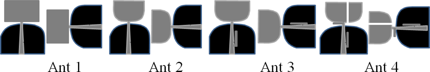
Fig. 2. Design evolution of the proposed antenna.

Fig. 3. Simulated return loss characteristics of antennas 1-4.

Fig. 4. Simulated S-parameters curve for with and without I-shaped slot.
Two feeding ports (port 1 and port 2) are employed to excite the X (horizontal) and Y (vertical) polarization, respectively. Two identical radiating elements are placed orthogonal with each other, in order to achieve the high isolation between two feeding ports (port 1 and port 2) over the SWB region. Our proposed structure provides high isolation without any additional isolation elements [Reference Kumar and Surushe18], which makes the design and fabrication of the antenna a bit simple. To validate the aforesaid points such as extremely large BW, dual band-notched functionality and high isolation, the simulated S-parameters have been depicted in Fig. 5. FromFig. 5 it is observed that the average isolation (|S 12|/|S 21|) between the two ports is <−30 dB across the frequency band of 1.2–25 GHz except for two rejected bands, which fulfills the essence of polarization diversity antennas. In addition, the simulated |S 11|/|S 22| with band-notched shows that the antenna starts operating from 1.2 to 25 GHz, except for the two rejected bands (denoted as |S 11|/|S 22| with band-notched) at 5–6 GHz and 7.25–8.5 GHz, respectively. The optimal dimensions (derived using Ansoft HFSS version 14) of the proposed antennas are as follows: L = 40 mm, W = 70 mm, M = 22 mm, N = 8 mm, I = 0.3 mm, V = 1 mm, p = 1.4 mm, B = 22.6 mm, W 3 = 31 mm, g = 7 mm, H = 23 mm, L 1 = 8 mm, T = 0.3 mm, C 1 = 0.3 mm, g 1 = 14.5 mm, g 2 = 9.6 mm, b = 1 mm, H 1 = 5.5 mm, q = 9.5 mm, r 1 = 8.32 mm, r 2 = 12.77 mm, C = 8.6 mm, A = 3 mm, D = 30 mm, and S = 0.5 mm.

Fig. 5. Simulated S-parameters of the proposed antenna.
Results and discussions
Current distribution
In order to observe the physical behavior of the proposed antenna at two notched bands 5.5 and 7.85 GHz, the simulated surface current distribution plot is shown in Fig. 6 when port 1 is excited and port 2 is terminated with a 50-Ω load.

Fig. 6. Simulated surface current distribution of the proposed antenna at (a) 5.5 GHz (b) 7.85 GHz when port 1 is excited.
Since both ports (port 1 and port 2) are symmetrical, therefore current distribution is shown only for port 1. As can be seen, that the currents are mainly concentrated (indicated by red color) on LOCS and HOCS at the two resonant frequencies 5.5 and 7.85 GHz respectively, which shows that the antenna offers high suppression of radiation characteristics at the notched frequencies. In other words, most of the energy is reflected back at the notched frequencies, owing to the presence of LOCS and HOCS, while at the other frequencies, the signal is transferred successfully to the radiating element.
Parametric study
To obtain an intensive insight of how the proposed antenna's dimensions effect the overall antenna performance, a parametric analysis has been carried out. Figure 7 displays the simulated return loss (|S 11|/|S 22|) of the proposed antenna for different N. From Figure 7 it can be seen that by decreasing N from 8 to 6 mm, the percentage BW of the antenna significantly reduces from 90.8 to 89.3. Therefore, the optimized value of N=8 was selected. Figure 8 plots the simulated S-parameters for different W 3. It is observed that decreasing the value of W 3 from 31 to 29 mm leads to worsening the performance of average isolation between port 1 and port 2 within the UWB region as well as high-frequency region. With the increase of W 3 from 31 to 32 mm, a high isolation (|S 21|/|S 12| ≥ 30 dB) can be obtained up to 13 GHz, whereas the performance of an average isolation reduces beyond 13 GHz. Therefore, favorable value of W 3 is set to be 31 mm to achieve the port isolation better than − 32 dB for the entire band. Figures 9, 10, and 11 shows how the key parameters S, H 1, and L 1, flexibly controls the two notched bands. From Figs 9 and 10 it can be observed that by increasing the values of S and H 1 from (0.2, 5 mm) to (0.8, 6 mm), the first notched band remains insensitive, however second notched band moves towards left side from 8.95 and 8.5 GHz to 6.85 and 7.2 GHz, respectively. From these outcomes, we can conclude that the notched frequency can be easily controlled by varying the value of H 1. Moreover, as shown in Fig. 11 increasing the value of L 1 from 7.5 to 8.5 mm with other parameters fixed results in a first notched band shifted from 5.3 to 6 GHz, whereas the second notched band remains insensitive. Therefore, the impedance BW of notch frequency is controllable by adjusting the values of H 1 and L 1.

Fig. 7. Simulated S-parameters of the proposed antenna for different N.

Fig. 8. Simulated S-parameters of the proposed antenna for different W 3.

Fig. 9. Simulated S-parameters of the proposed antenna for different S.

Fig. 10. Simulated S-parameters of the proposed antenna for different H 1.
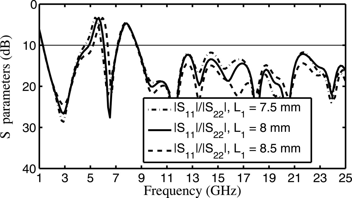
Fig. 11. Simulated S-parameters of the proposed antenna for different L 1.
Equivalent circuit
Figure 12 represents the simulated input impedance of the proposed antenna. As shown in Fig. 12, by introducing a pair of open-circuited stubs two anti resonances are introduced at 5.5 and 7.85 GHz. The real part of the impedance of antenna at the frequency where the reactance is zero is called the resonant frequency. At notched frequency 5.5 GHz, the real part of the input impedance is maximum (150-Ω), when its imaginary component graph is zero crossing (behaves as a parallel LC resonator). However at frequency 7.85 GHz, the real component is minimum (approximately close to zero) and imaginary component graph behaves as a series LC resonator. On the other hand in the pass-band frequencies the reflection coefficient |S 11| < −10 dB can be achieved owing to multiple resonances excited by the proposed SWB antenna and each resonance can be considered as a parallel RLC circuit. The series and parallel LC resonators shown in Fig. 13 denote the contribution of the two notches, whereas several parallel RLC resonators are responsible for the wide impedance BW. The equivalent circuit input impedance can be represented as [Reference Moradikordalivand, Rahman, Ebrahimi and Hakimi19]
 $$ {Z_{in}} = {Z_p} + {Z_s} + \mathop \sum \limits_{n = 1}^\infty \displaystyle{{{\,j\omega .{R_k}.{L_k}}}\over{{{R_k}.\left( {1 - {\omega ^2}.{L_k}.{C_k}} \right) + j\omega .{L_k}}}},$$
where
 $$ {Z_p} = \displaystyle{{{\,j\omega {L_p}}}\over{{\left( {1 - {\omega ^2}{L_p}{C_p}} \right)}}},$$
 $$ {Z_s} = \displaystyle{{{\,j({\omega ^2}{L_s}{C_s} - 1)}}\over{{\omega {C_s}}}}.$$
Fig. 12. Input impedance of the proposed antenna.

Fig. 13. Equivalent circuit model of the proposed antenna.
Experimental results
The proposed antenna's layout is presented in Fig. 14. The measured impedance BW of the proposed antenna is carried out by a Rodhe and Schwarz ZVA24 vector network analyzer. Figure 15 shows a reasonably good agreement between the measured results and the simulated one across the specified frequency range from 1.2 -to 25 GHz with dual notched band of 5–6 GHz and 7.2–8.5 GHz, respectively.

Fig. 14. Photograph of the fabricated antenna.

Fig. 15. Simulated and measured S-parameters of the proposed antenna.
Diversity performance
The diversity performance of the proposed antenna can be evaluated by computing the envelope correlation coefficient (ECC) from the radiation pattern as described in [Reference Jaafreh, Huang and Xing20]. The purpose of calculating the value of ECC is to estimate how much the communication channels of the proposed antenna are isolated to each other. For reasonably well diversity performance of an antenna pair, the value of ECC should be <0.5 and can be estimated using far-field radiation pattern-based formula stated below [Reference Jaafreh, Huang and Xing20]
 $$ \rho = \displaystyle{{{\left\vert {\int \!\!{\int_{4\pi } {{{\overrightarrow E }^1}(\theta {\rm{,}}\phi ) \bullet {{\left( {{{\overrightarrow E }^2}(\theta {\rm{,}}\phi )} \right)}^{\ast}}d\Omega } } } \right\vert}}\over{{\sqrt {\int \!\!{\int_{4\pi } {{{\left\vert {{{\overrightarrow E }^1}(\theta {\rm{,}}\phi )} \right\vert}^2}d\Omega \int \!\!{\int_{4\pi } {{{\left\vert {{{\overrightarrow E }^2}(\theta {\rm{,}}\phi )} \right\vert}^2}d\Omega } } } } } }}},$$
where  ${\overrightarrow E ^i}(\theta {\rm {,\,}}\phi ) = E_\theta ^i\widehat \theta + E_\phi ^i\widehat \phi $ is the radiation field of the antenna system when i th port is excited, and
  ${E_\theta }$ and
  ${E_\phi }$ are the components in the direction of
  ${\widehat \theta }$ and
  ${\widehat \phi }$, respectively. The simulated result of ECC is plotted in Fig. 16. It is observed that over the entire frequency band (including two notches) correlation coefficient is below 0.025 which satisfies a good diversity performance.

Fig. 16. ECC of the proposed antenna.
Radiation pattern and gain
A peak gain is measured by gain transfer technique [Reference Stutzman and Thiele21] where a typical broadband horn antenna was utilized to radiate the total power to the proposed antenna. Figure 17 illustrates the simulated and measured outcomes of the proposed antenna. The measured antenna gain shown in Fig. 17 is reduced to − 5.2 and − 4.1 dBi in the two stopbands from 5 to 6 GHz (WLAN) and 7–8 GHz (X-band satellite communication), respectively. However, the average gain of the proposed antenna beyond the notched bands is about 4.8 dBi. Table 1 depicts the dimension, ratio BW and isolation of the proposed antenna with existing antennas. The simulated and measured 2D far-field radiation patterns for port 1 of the proposed antenna in the E-plane (xy-plane) and H-plane (xz-plane) at 3.1, 10.6, and 20 GHz are shown in Fig. 18. Since both the ports are identical, therefore in the Fig. 18 port 1 is excited, while port 2 is terminated by a 50-Ω. It is evident that the H-plane (xz-plane port 1 and xy-plane port 2) patterns are nearly omnidirectional and relatively stable (variation is <− 10 dB) at frequencies 3.1 and 10.6 GHz. The E-plane (xy-plane port 1 and xz-plane port 2) radiation patterns at 3.1 and 10.6 GHz are directed maximum towards − Y-direction, showing the dipole-like (figure- of-eight) radiation patterns. The cross-polarization levels are approximately − 20 dB in the E- and H-planes at 3.1 and 10.6 GHz. However, in the E- and H-planes, it can be observed that at 20 GHz the cross-polarization level rises. Moreover, since the port 1 (vertical polarization) and port 2 (horizontal polarization) are oriented by 90° with each other, therefore the proposed antenna generates a considerably well orthogonal polarization performance.

Fig. 17. Simulated and measured gain of the proposed antenna.

Fig. 18. Simulated (red) and measured (black) 2D far-field radiation patterns of the proposed antenna for different frequencies (a) 3.1 GHz (b) 10.6 GHz, and (c) 20 GHz (solid line is co-polarization and dashed line is cross-polarization).
Table 1. Comparison of the size, BW, and isolation of the proposed antennas with other antennas

Time domain characteristics
Group delay [Reference Lee, Kwon, Kang and Lee22] is one of the most important parameter in communication system, which shows the degree of distortion of SWB pulse. Group delay is the measure of a signal transition time through a device. It is measured by keeping two identical antennas at a distance of 60 cm in the far field region in face-to-face and side-by-side orientations. The measured group delays for the face-to-face and side-by-side antenna results over the frequency from 1 to 25 GHz is presented in Fig. 19. From the graph, we can observe that the group delay is increased in the notch band, however variation of group delay is <0.7 ns outside the notched-band.

Fig. 19. Group delay of the proposed antenna.
Conclusion
A compact SWB polarization diversity printed monopole antenna with dual band-notched functionality has been investigated in this communication. The proposed antenna provides an extremely large impedance BW in the frequency band of 1.2–25 GHz (ratio BW of 20.8:3) with dual band-notched characteristics covering the WLAN band and X-band satellite communication.To achieve the isolation better than − 30 dB (low mutual coupling) in the SWB band, two identical monopole antennas have been placed orthogonal to each other at a distance of 1 mm. Moreover, The proposed antenna possesses minimum ECC of 0.025 over the SWB frequency range, authenticating it a suitable candidate for polarization diversity applications. Due to large BW this antenna may also be used for spectrum sensing in cognitive radio [Reference Grayaver23].
 Murli Manohar received the Ph.D. degree in Electronics and Electrical Engineering from the Indian Institute of Technology Guwahati, India in April 2015. He is presently working as an assistant professor in the Dept. of Electronics and Communication Engineering, Indian Inst. of Information Technology Manipur, India. His main research area is in antenna and RF engineering with focus on SWB printed monopole antenna.
 Rakhesh Singh Kshetrimayum received the Ph.D. degree from the School of Electrical and Electronic Engineering (EEE), Nanyang Technological University (NTU) Singapore in 2005. Since 2005, he has been with the Dept. of EEE, IIT Guwahati as an Associate Professor (2010-), Assistant Professor (2006–10) and Senior Lecturer (2005–2006). He worked as a Postdoctoral Scholar at the Dept. of EE, Pennsylvania State University (PSU), USA (2005), Research Associate Provisional at the Dept. of Electrical Communication Engineering (ECE), Indian Inst. of Science (IISc) Bangalore (2004–2005), Teaching Assistant at the School of EEE, NTU Singapore (2002–2003) and Trainee Software Engineer at Mphasis, India (2000–2001). Dr. Kshetrimayum is the recipient of SEFOGG Young Engineer Award (2011), Dept. of Science & Technology India (SERC) Fast Track Scheme for Young Scientists (2007–2010) and NTU Research Scholarship from 2001–2004. His current areas of research interests are in printed antennas and circuits, UWB communications and MIMO wireless communications. He has been involved in organizing several IEEE international conferences as Technical program co-chair, Publication chair, Program chair, Session chair and Technical program committee. He is the Editor-in- Chief of Inderscience journal International Journal of Ultra Wideband Communications and Systems. He is a Life Fellow of the Institution of Electronics and Telecommunication Engineers (IETE), India, Optical Society of India (OSI) and Antenna Test & Measurement Society (ATMS), India; a senior member of the International Association of Computer Science and Information Technology (IACSIT), Singapore, and the Inst. of Electrical and Electronics Engineers (IEEE), USA; a member of the Applied Computational Electromagnetics Society (ACES), USA and the European Microwave Association (EuMA), Belgium.
 Anup Kumar Gogoi is a Professor of Electronics and Electrical Engineering and Dean of Outreach Education Programme at the Indian Institute of Technology Guwahati. He received his Ph.D. degree from the Dept. of Electrical Engineering, Indian Inst. of Technology Kanpur. His areas of research interests are in electromagnetics, microwave engineering, RF circuits, and systems design.


