I. INTRODUCTION
In recent years, with the improvement of millimeter-wave (MMW) device's level, circuit design technology, antenna technology, and so on, the MMW technology has been greatly developed and widely used in some relevant areas, such as radar detection, high-speed communications, missile guidance, satellite remote sensing, electronic countermeasure, etc. [Reference Heddebaut, Elbahhar, Loyez, Obeid, Rolland and Rivenq1]. This has brought a large demand for high-performance MMW frequency synthesizer. As one of the most important blocks in a transceiver, a frequency synthesizer, which can provide a clean, stable, and programmable local oscillator (LO) signal, is greatly desired [Reference Cai, Yang, Yuanwang and Liu2].
The MMW system was required not only extracting the information of target location and speed, but also analyzing and identifying the target. Beyond centre frequency and bandwidth, a highly linear frequency modulated (LFM) and a very low phase noise of the MMW signal are the most relevant features to be carefully considered for a proper system design. Both aspects are substantially defined by the frequency synthesizer [Reference Hasenaecker, van Delden, Jaeschke and Pohl3]. So, the MMW frequency synthesizer needs to generate and receive signals with broadband, frequency agility, high-resolution, multi-LFM mode [Reference Patton and Rigling4]. At present, the MMW frequency synthesis architectures mainly include phase-locked loop (PLL) with a voltage-controlled oscillator (VCO), direct digital frequency synthesizer (DDS) driving PLL, DDS interpolation in PLL loop, and DDS frequency up-conversion [Reference Zhao, Li and Chang5]. In MMW systems, although the PLL synthesizers are full used widely in various electronic systems, they cannot achieve low phase noise and fast switching speed, while its reference frequency becomes low at small frequency step. DDS can generate very linear and agile frequency chirps, assuming a high-quality and constant frequency reference clock source, but its output frequency cannot reach MMW band, the frequency resolution and purity will be deteriorated by using the PLL to frequency multiply. DDS interpolation in the PLL loop method can improve the phase frequency and the time of frequency agility, but the circuit becomes complex, the loop is unstable, so it is hard to debug. The DDS frequency up-conversion architecture has wide output frequency, fast frequency agile time, and its purity of spectrum will not deteriorate more than the DDS.
In this paper, a scheme of MMW frequency synthesizer was designed by using the advantages of DDS and PLL, based on the direct hybrid frequency synthesis. It includes frequency multipliers, filters, mixers, and switches. The LFM signal is generated by the DDS, and is converted to a different center frequency by agile LOs.
II. FREQUENCY SYNTHESIZER SYSTEM DESIGN
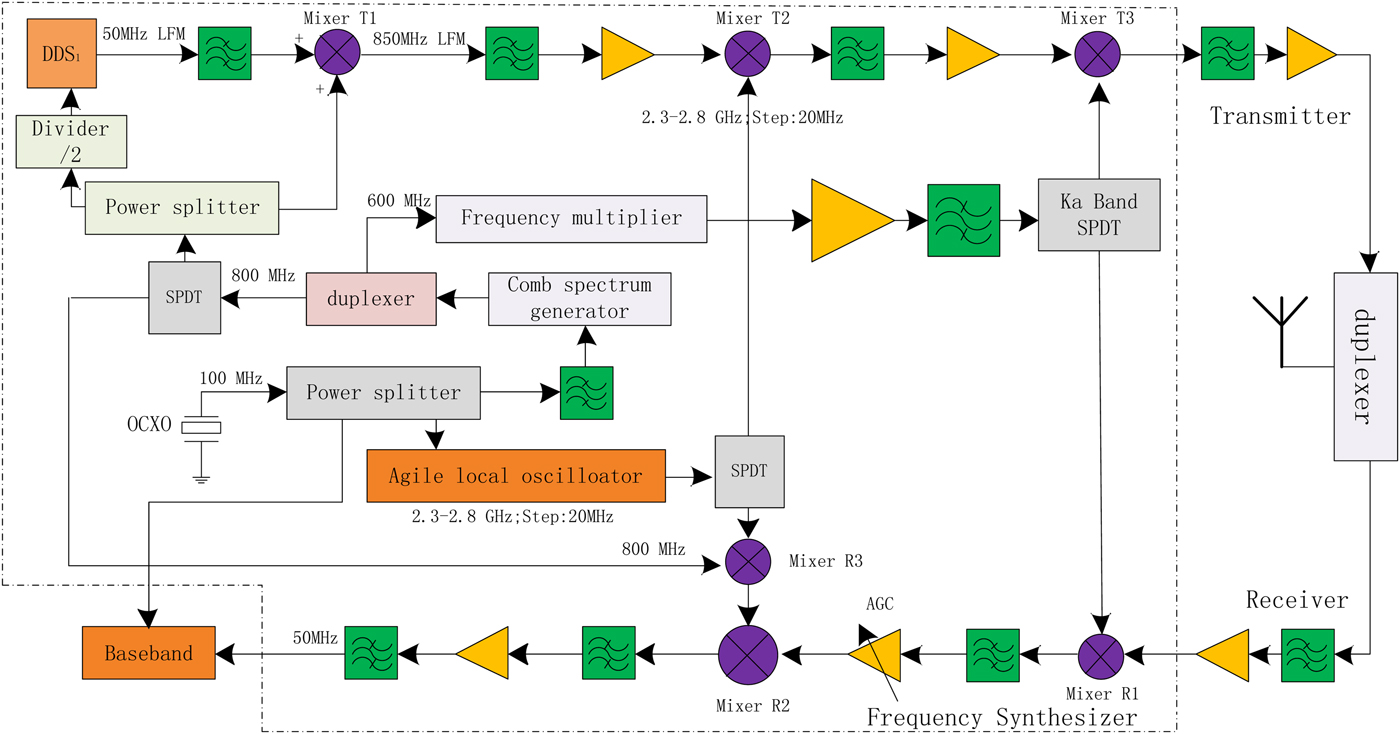
By analyzing the performance of various frequency synthesis and the requirements of system function norm, taking into account the working frequency, bandwidth, phase noise, and frequency-hopping time index is the key to design the framework of the system, the system block diagram of MWW frequency synthesizer is presented in Fig. 1 [Reference Ma and Tang6, Reference Simons and Wintucky7], which use DDS frequency up-conversion. The modules in the dotted line are part of the frequency synthesizer.

Fig. 1. System block diagram of the proposed MMW frequency synthesizer.
In order to ensure the coherence of the system, the clock signal is provided by a single 100 MHz oven-controlled crystal oscillator. Firstly, the 600 and 800 MHz point frequency signal is generated by the comb spectrum generator, and extracted from the duplex. Then the 600 MHz signal is multiplied to MWW band by frequency multiplier, the Ka-band mixer's LO signal is filtered after frequency multiplier. The 800 MHz signal provides the first LO signal for the transmitter and receiver. Sinusoidal signals or LFM signals are generated by the DDS core, and up-converted to MWW band signals after three times. The second intermediate frequency (IF) LOs are provided by the 800 MHz signal and agile LO, which has 20 MHz steps.
III. KEY MODULES DESIGN
A) LFM generation
DDS is one of the most ideal devices to produce LFM signal. Since this design requires two DDS cores, so we use AD9958 in this system. There are two accumulators in one of DDS cores: phase accumulator and frequency accumulator. Each phase increment corresponds to the DDS output frequency, and the phase increment value (frequency tuning word K) is proportional to the frequency. So the output frequency of each DDS channel is a function of the rollover rate of each phase accumulator. The slope of the LFM signal is determined by the frequency accumulator-accumulated rate. The accumulators can generate the high-speed LFM signal, which is called quadratic time base signal.
When the DDS phase was truncated, the spurious-free dynamic range (SFDR) performance can be calculated by the below formula [Reference Jun-an, Guang-jun, Rui-tao, Jiao-xue, Ya-feng and Bo8]:
 $$\eqalignno{&(SFDR)_{dB} \cr &\quad = 20 \cdot \lg \left\{ {\left[ {\pi Sa\left( {\displaystyle{{f_{out}} \over {f_S}} \pi} \right)} \right]/\left[ {\pi 2^{ - P} Sa\left( {\displaystyle{{f_{out}} \over {f_S}} \pi} \right) \cdot Sa\left( {\displaystyle{{f_1} \over {f_S}} \pi} \right)} \right]} \right\} \cr &\quad =20 \cdot \lg \left[ {2^P /Sa\left( {\displaystyle{{f_1} \over {f_S}} \pi} \right)} \right] \ge 6.02 \cdot P,}$$
Where Sa(·) is a sample function, P is the bit of the sine lookup ROM table in the DDS core. AD9958 has 14 bits of ROM, so the narrow-band SFDR can reach 84 dBc, which is more than 70 dBc. The nonlinearity of DAC is the main source of AD9958's large spur.
In order to reduce the far end of DDS output spurious signal and suppress the harmonics, which is caused by the non-linearity of the amplifier, a band pass filter (BPF) can be added after the DDS, whose center frequency is 50 MHz, and bandwidth is 10 MHz. The BPF is designed and shown in Fig. 2, the typical performance is measured by network analyzer R&S@ZVL3, and the results are shown in Fig. 3. The pass band insertion loss is <3.4 dB, the stop band insertion loss is more than 40 dB.
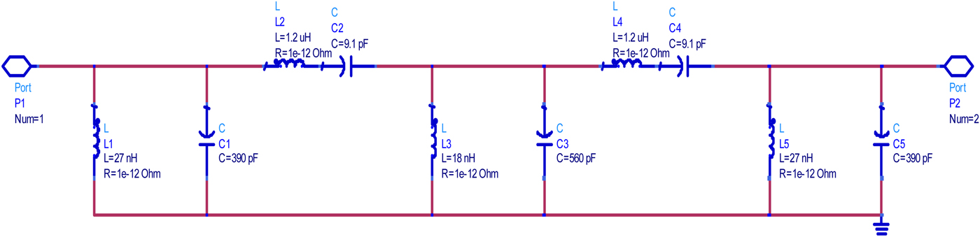
Fig. 2. The circuit of 45–55 MHz BPF.
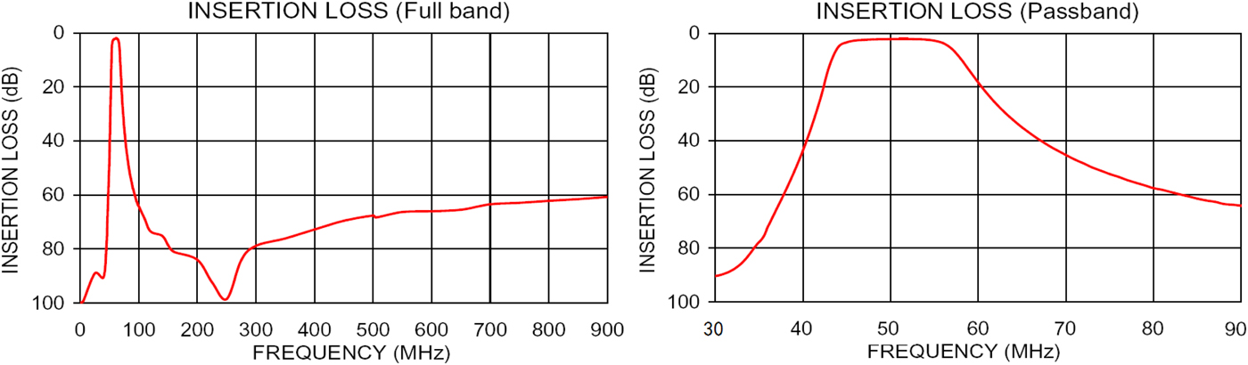
Fig. 3. Typical performance measured results of 45–55 MHz BPF.
B) Agile and low phase noise LO design
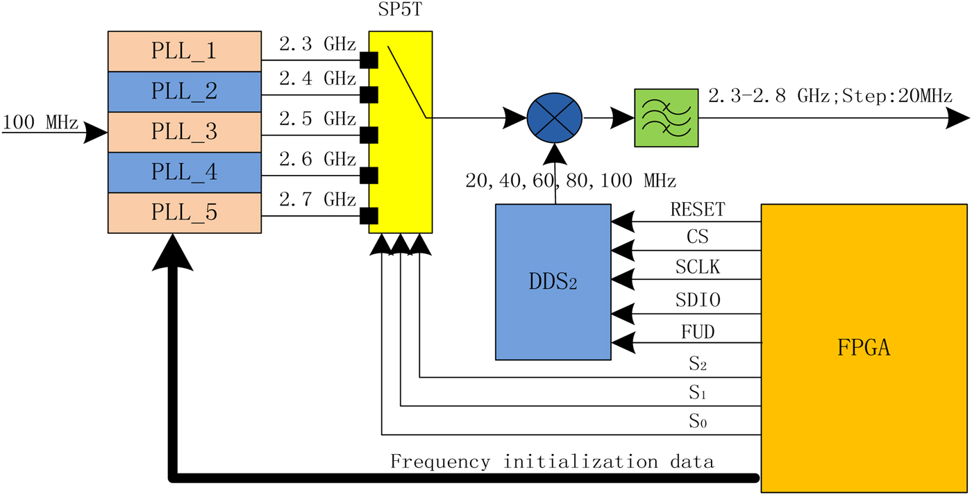
The system required 20 MHz frequency interval in the 500 MHz bandwidth, and the frequency agility time is <2 µs, the index is relatively high, so this is a key technical problem of this subject. Therefore, five PLLs mini-module were used to generate five 100 MHz steps fixed frequency signals, and DDS2 generate 20 MHz steps frequency signals. The desired agile LO is selected by the switch that is controlled by the high-speed FPGA. Schematic of LOs switching is shown in Fig. 4. So, the agile LO frequency can be got:
 $$f_{agile{\rm} \,LO} = f_{PLL} + f_{DDS}, $$
where f PLL is the output signal frequency of PLL, and f DDS is the output signal frequency of DDS.

Fig. 4. Schematic diagram of agile LO.
To describe the noise specification of PLL, the phase noise model diagram of PLL can be given as Fig. 5, where θ i (s), θ o (s), θ P (s), θ F (s), θ D (s), and θ VCO (s) represent the phase of reference signal, output signal, phase noise of phase frequency detector (PFD), loop filter, frequency divider, and VCO, respectively. The corresponding phase noise power spectrum density functions (PSD) are s φi (f), s φo (f), s φP (f), s φF (f), s φD (f), and s φVCO (f). The phase noise of output signal of PLL can be given as [Reference Yang, Dan, Cai and Ma9]:
 $$\eqalign{s_{\varphi o} (f) = \; & \left[ {s_{\varphi i} (f) + \displaystyle{1 \over {K_d^2}} s_{\varphi P} (f) + N^2 s_{\varphi D} (f)} \right]\left \vert {H(j\omega )} \right \vert \cr & \quad + \left[ {\left \vert {\displaystyle{{K_{VCO}} \over \omega}} \right \vert ^2 s_{\varphi F} (f) + s_{\varphi VCO} (f)} \right]\left \vert {H_e (j\omega )} \right \vert ^2,} $$
where H(jω) and H e (jω) represent PLL forward transfer function and PLL error transfer function, respectively.
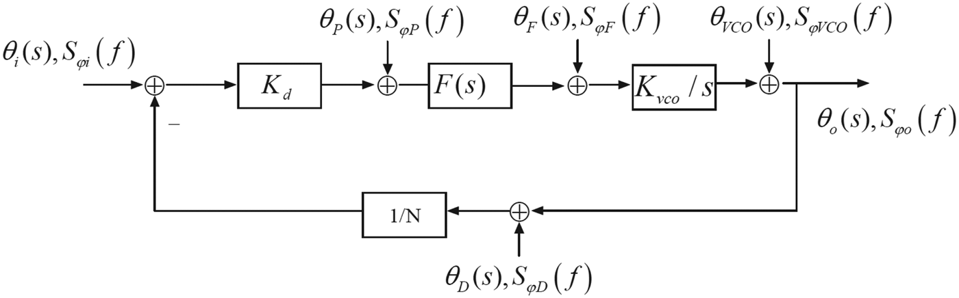
Fig. 5. Noise model of PLL.
From (3) it can be concluded that the phase noise of PLL is comprised of two parts. The phase noise within the band width of loop filter is mainly determined by the phase noise of reference signal and the phase noise of VCO will decide the phase noise outside the loop bandwidth of PLL. The loop bandwidth can be given as:
 $$K = K_\varphi \cdot K_{VCO}^{\prime} \cdot K_f = K_\varphi \cdot K_{VCO} \cdot \displaystyle{{K_f} \over N},$$
where K φ, K f , K VCO , and N denotes the gain of PFD, gain of loop filter, gain of VCO, and frequency divide, respectively.
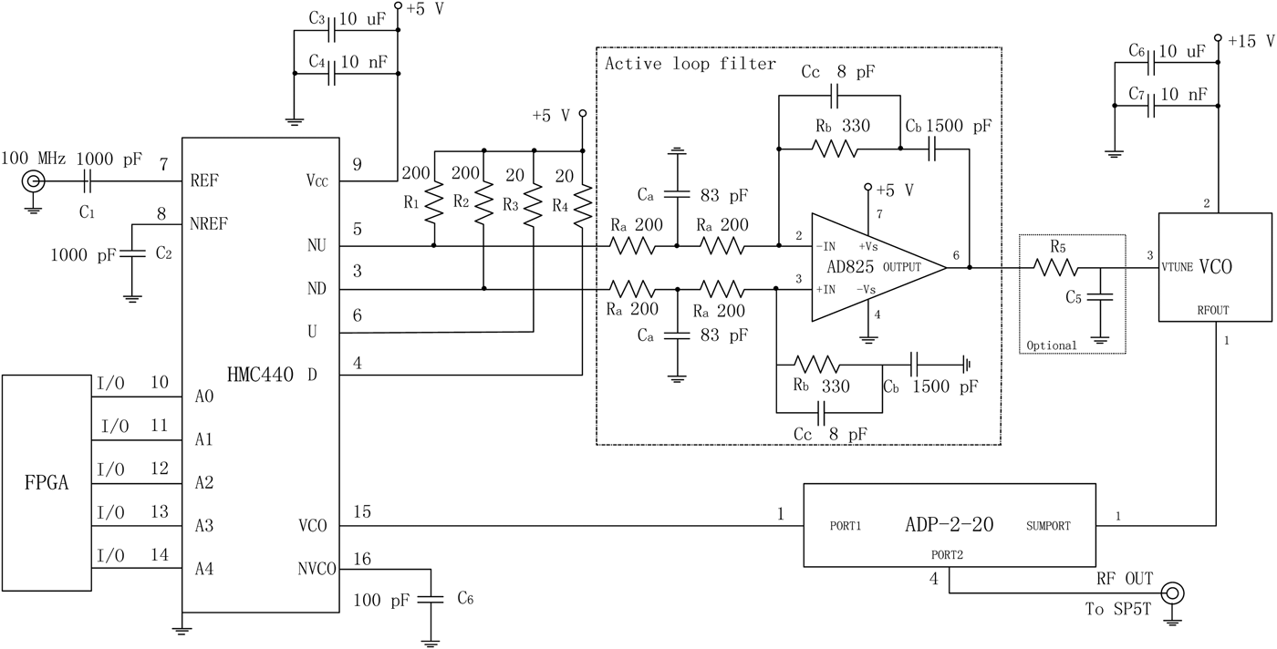
To achieve stable spectrum purity of agile LO, the HMC440 chip is used to build the PLL circuit, which has ultra low SSB Phase Noise Floor (−153 dBc/Hz@10 kHz offset @ 100 MHz reference frequency). The circuit diagram of the PLL is shown in Fig. 6. Because the HMC440 chip's PFD has differential output signal, we use the active loop filter, which has differential input and single-ended output. In the active loop filter, the AD825 is a superbly optimized operational amplifier. The role of C c is to reduce the high frequency of PFD output signal, its capacity value is generally in the picofarads level, and C a and C b capacity value is bigger than C C . According to the PLL transfer function, we can get:
 $$C_a = \displaystyle{2 \over {R_a K}}\sqrt {\displaystyle{{1 - \sin \varphi} \over {1 + \sin \varphi}}}, $$
 $$C_b = \displaystyle{{K_\varphi \cdot K_{VCO}} \over {2N \cdot K^2 \cdot R_a}} \sqrt {\displaystyle{{1 + \sin \varphi} \over {1 - \sin \varphi}}}, $$
 $$R_b = \displaystyle{1 \over {C_b \cdot K}}\sqrt {\displaystyle{{1 + \sin \varphi} \over {1 - \sin \varphi}}}, $$
where φ is the phase margin of PLL. If loop bandwidth is set to 250 kHz and phase margin is set to 75°, we can get C a = 83, C b = 1500 pF, R b = 330 Ω, C c = 8 pF.

Fig. 6. Circuit diagram of the PLL.
If the PFD ripple is too high, we can add a passive first-order low-pass filter, which is composed by R 5 and C 5. So, the first-order low-pass filter is option, we can design it in the printed circuit board (PCB). The required PLL phase noise curve can be obtained as shown in Fig. 7. The simulation of total curve is simulated by ADIsimPLL software, the phase noise is about −103 dBc/Hz@1 kHz offset @ 2.5 GHz center frequency; and the measured curve is measured by a R&S FSUP signal source analyzer, the measured phase noise is about −101.45 dBc/Hz @1 kHz offset @ 2.5 GHz center frequency. The curve is slightly different because of the component values are a little deviate.
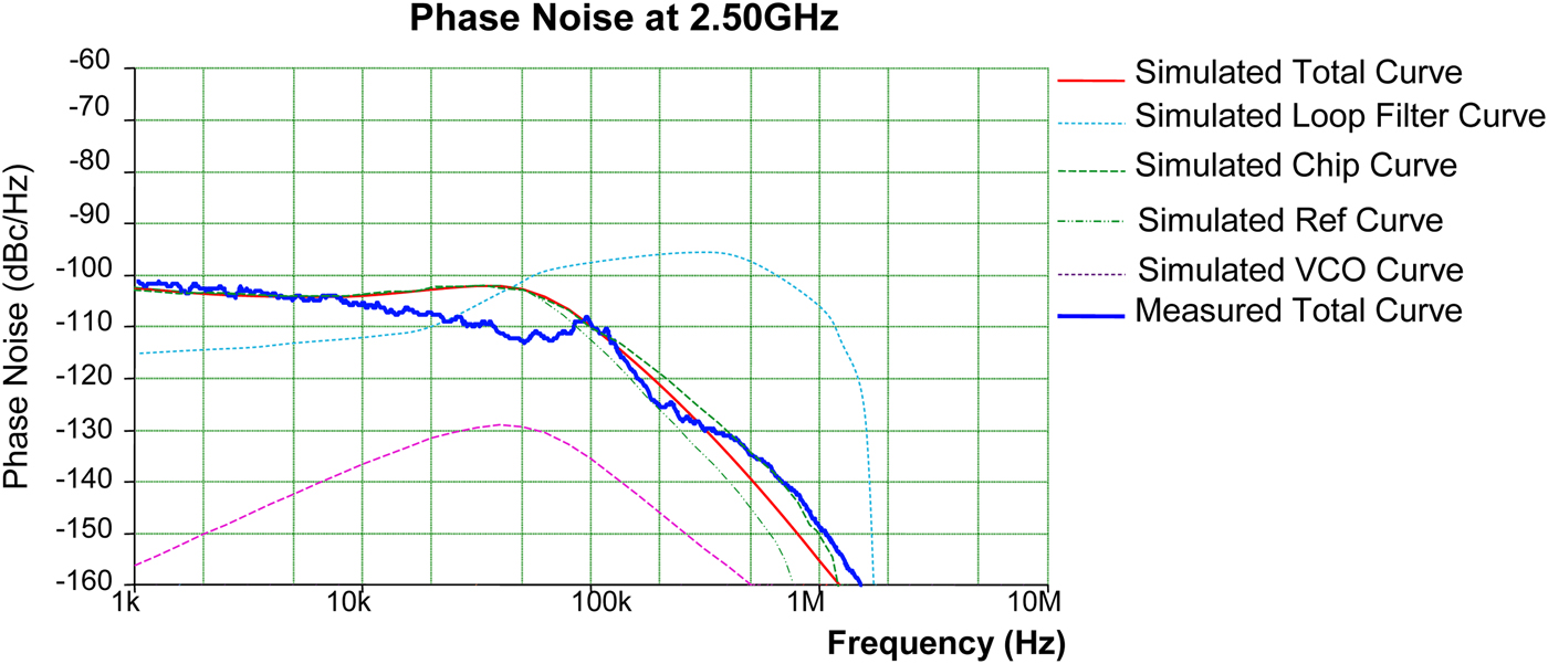
Fig. 7. Simulated and measured curve of the required PLL phase noise.
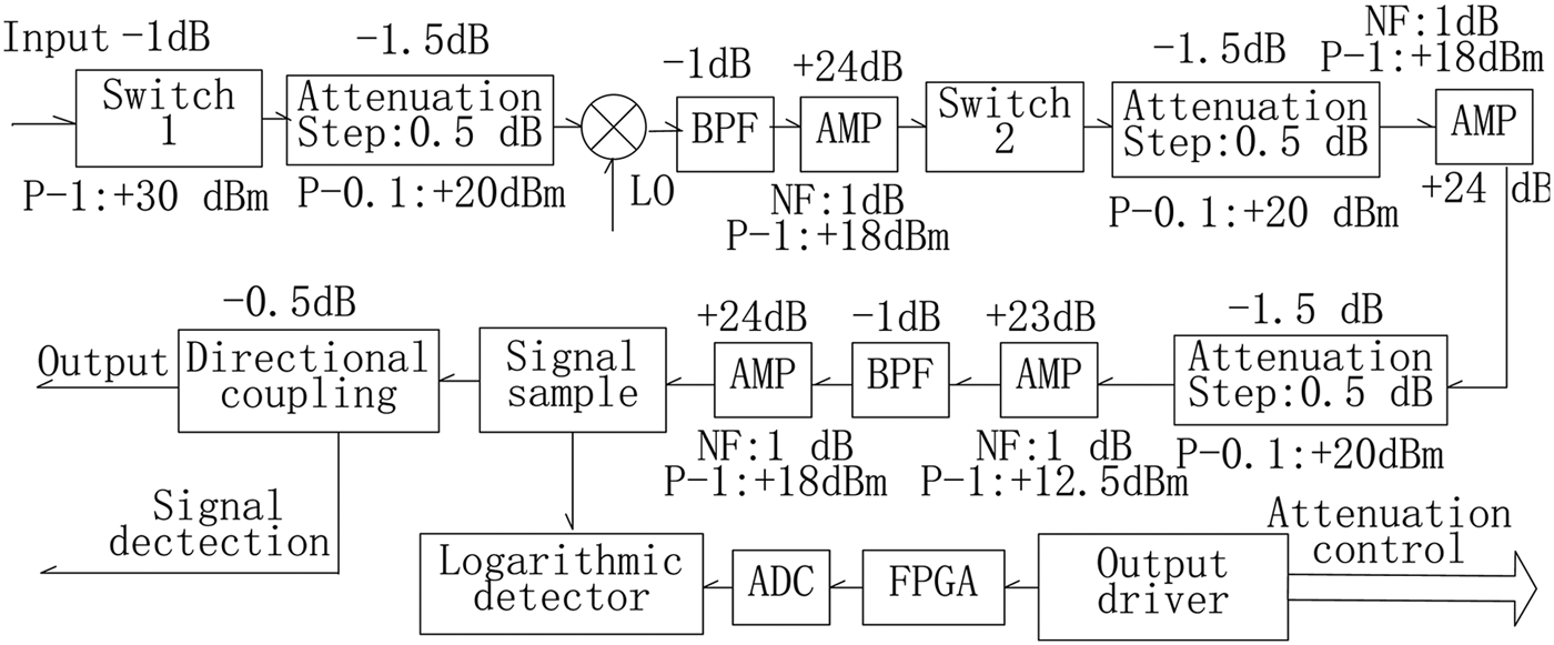
C) Automatic gain control and receiver front-end circuit
Because of the different strength signals are received, the receiver needs to add the automatic gain control (AGC) circuit in the IF part. In order to eliminate the high “flag” voltage, and avoid IF amplifier entering saturation state, the switch 2 was added in receiver link. Signal sampling circuit was used to sample the signal power and control the step attenuations. The design of AGC parameters are shown in Fig. 8.

Fig. 8. Design of AGC parameters in receiver.
To ensure the total gain and noise figure of the receiver meet the requirements of the technical protocol, receiver front-end circuit is shown in Fig. 9. The isolation of the protective switch is 40 dB, IF power amplifier is composed of four-stage low-noise high-gain amplifier. There are three digital attenuators. Because of the maximum input level is 15 dBm and 1 dB compression point of mixer is 10 dBm, the first attenuation is lied before the second mixer, to ensure the mixer work normally in a large input signal. The other two stages of the attenuator are inserted between the amplifiers. So, there are eight stages in the AGC, whose gain is 80 dB, noise figure is 13.01 dB, and input third-order intercept point is 14.85 dBm. The AGC index satisfies the requirements well.
Fig. 9. Receiver front-end circuit.
D) MMW LO circuit
The MMW LO is generated by frequency multiplier as in Fig. 10. CHX2092A and HMC283 were used in frequency quadruple and amplitude amplification for MMW signal.
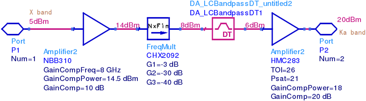
Fig. 10. MMW LO circuit schematic diagram.
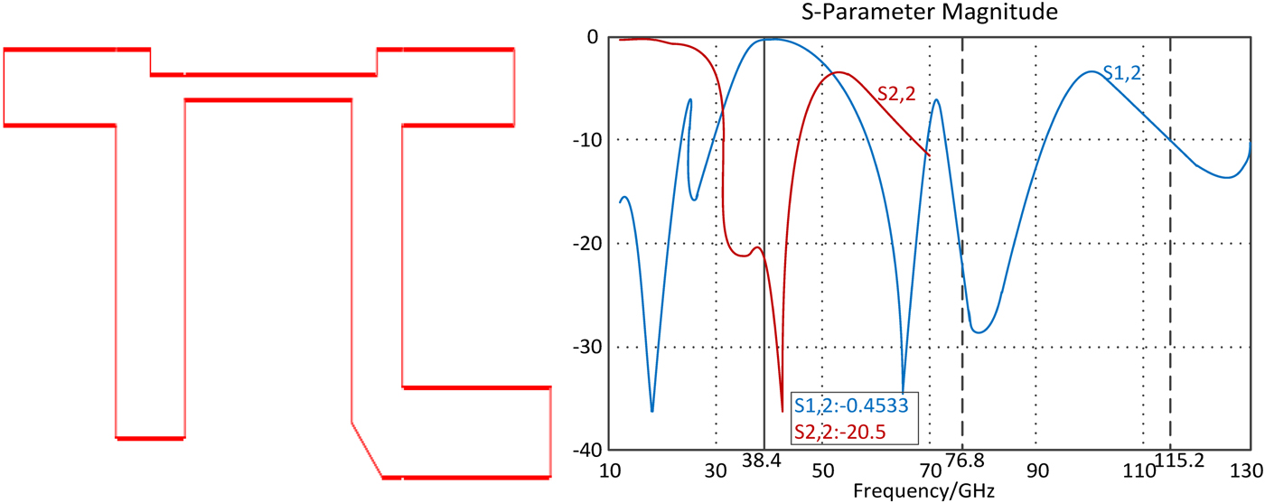
There are a lot of harmonic signals after the frequency quadruple, so MMW filter is necessary to control the harmonic. The MMW filter mainly considers the harmonic of the output signal; therefore, aluminum nitride film ceramic substrate materials and open stub method are used in micro strip transmission lines, its S parameters are simulated by HFSS software as shown in Fig. 11, there is 25 and 10 dB of the attenuation at the two harmonic and the three harmonic, so the branch micro strip filter satisfy the requirement of higher harmonic.

Fig. 11. Open-circuit branch micro-strip filter and S parameter simulation results.
IV. EXPERIMENTAL RESULTS
The main test equipment includes: Agilent E4447A spectrum analyzer and R&S FSUP signal source analyzer. The size of total frequency synthesizer is <200 × 150 × 50 mm3. Figure 12 shows the PCB test board and indicates the circuit blocks by nearby text, there are two sides of the cavity.

Fig. 12. PCB test board.
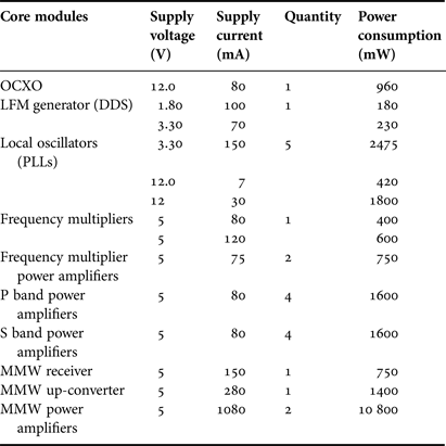
Power consumption of the core modules are summarized and listed in a Table 1. Some modules used multiple power supply, such as DDS, PLL, etc. There are two kinds of power supply voltages, which are +12, +5 V in the whole-frequency synthesizer system, so low dropout linear regulators LT1965 were used to generate the +3.3 and +1.8 V, the power consumption of total frequency synthesizer is about 28 W.
Table 1. Power consumption of the core modules.

Figure 13 shows the phase noise and spurious suppression performance of whole MWW synthesizer, which are less than −80 dBc/Hz@1 kHz and −65 dBc. Figure 14 show LFM output of the MWW synthesizer and frequency-hopping time, the maximum frequency-hopping time is <1.8 µs. All of the test results satisfy comprehensive performance.
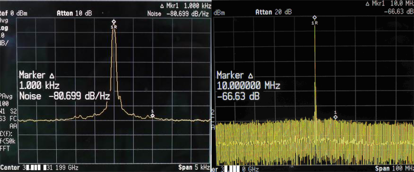
Fig. 13. Phase noise and spurious suppression performance.
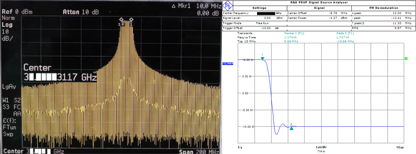
Fig. 14. LFM output of the synthesizer and frequency-hopping time.
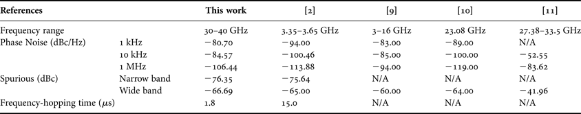
Table 2 summarizes the performance of the proposed frequency synthesizer and compares it with the relevant state-of-the-art [Reference Cai, Yang, Yuanwang and Liu2, Reference Yang, Dan, Cai and Ma9–Reference Nam, Son and Shin13]. There are a few reported that a wideband MWW frequency synthesizer has low phase noise, low spurious, and frequency agility characteristics in recent years. In Cai et al. [Reference Cai, Yang, Yuanwang and Liu2] have the better phase noise and spurious performances, but its output frequency is lower and the frequency-hopping time is slower Yang et al. [Reference Yang, Dan, Cai and Ma9] used the architecture of PLL with a VCO, and did not consider frequency agility characteristics Yeh and Chang [Reference Yeh and Chang10] designed and analyzed a K-band low phase noise PLL with the sub-harmonically injection-locked technique, but it cannot improve the loop lock time. The MMW PLL synthesizer employing a wide-locking range is designed by the injection-locked frequency divider in [Reference Kang, Chien and Niknejad11, Reference Zhang, Shi and He12], but the performance is not better than this work. A double conversion mechanism composing of direct digital frequency synthesis, double-frequency chains and PLL is proposed in this work, and realized a system of MWW frequency synthesizer for wide band Radar with fast frequency switching. The design demand of frequency synthesis in radar transceiver is considered fully, on the condition that guarantee spectrum purity, using PLL produce LO with fast frequency switching, we find a perfect solution that convert a low, narrowband, linear sweep, and pulse-modulated single with center frequency of 50 MHz to MMW with 500 MHz bandwidth, and the hopping frequency bandwidth is 10 GHz.
Table 2. Performance comparison with the state-of-the-art frequency synthesizer.

V. CONCLUSION
The MMW frequency synthesizer scheme is presented in this paper, take account of spectral purity, frequency-hopping time, etc., its experimental results indicate that such frequency synthesizer has nice performance characteristics; it provides an important guarantee for the MWW transceiver. The method of frequency conversion, hopping, and the use of DDS and PLL-mixed design thought have important reference value for the design of low phase noise, frequency agile synthesizer.
ACKNOWLEDGEMENTS
The author would like to express a sincere appreciation to the editor and reviewer for their helpful comments in improving the presentation and quality of the paper. This work was supported by the Industry University Cooperation Project of Chinese Ministry of Education: Intelligent Electronic System Design.
 Qianhua Fu received the B.S. degree in Electronic Information Engineering from Chongqing University of Technology, China, in 2003, and received the M.S. degree in Communication and Information Systems from the University of Electronic Science and Technology of China (UESTC) in 2010. He was a R&D Engineer in HUAWEI Company from 2010 to 2014. He is currently pursuing the Ph.D. degree in Information and Communication Engineering, UESTC and working as an engineer at Xihua University. His main research interests are RF circuits and systems for wireless communications, signal processing in modern communication, memristor neural network, etc.