


Introduction
A substrate integrated waveguide is a planar integrated waveguide circuit, which is filled by dielectric and acts as a high-quality factor rectangular metallic waveguide. This structure can be easily fabricated using the printed circuit board (PCB) process which is a technological breakthrough. From the electromagnetic (EM) point of view, a substrate integrated waveguide (SIW) is almost equivalent to a metallic waveguide (MWG). The low-profile and ease of construction with minimal fabrication tolerances made SIWs suitable for several applications from microwave transceivers to radar systems. A wide range of SIW applications including active and passive microwave and mm-wave components are reported in [Reference Bozzi, Georgiadis and Wu1–Reference Li, Hong, Hua, Chen, Wu and Cui6]. Slotted waveguide array antennas are a key component in radar and range finder systems due to their advantages such as low side lobe level (SLL) and high directive radiation pattern. With the trend of the high-speed data rate in tracking radars, having a highly directive beam radar becomes necessary. There are several reports in the literature on using slot array in mono-pulse applications. A planar mono-pulse antenna array for C-band radar has been presented in [Reference Yu, Wang and Zhang7]. A wideband mono-pulse comparator as the antenna feed network has been applied for this C-band antenna operating in 5.05 ~ 6.675 GHz. An SIW slot array mono-pulse antenna which used a microstrip hybrid ring to act as a comparator has been proposed in [Reference Yan, Hong and Wu8].
In [Reference Elliott9], Elliot proposed a set of formulations based on the excitation control method for SLL suppression in a linear slotted array. In several slotted SIW antenna works, the initial design parameters have been obtained by Elliot's approach [Reference Elliott9] with further optimizations by full-wave EM packages. in [Reference Hosseininejad, Komjani and Mohammadi10], the impedance matching and pattern synthesis for a planar SIW slotted array has been performed using the initial design techniques reported in [Reference Elliott9] and the Method of Least Square (MLS) errors. A low SLL slotted waveguide antenna has been synthesized using Schelkunoff's unit circle method combined with genetic algorithm technique operating in X-band radar applications [Reference Kumar, Kedar and Kumar Singh11]. A compact double layer 8-cell SIW array antenna with circular polarization characteristics has been reported for mono-pulse applications. An improved rat-race-based feed network has been utilized to generate sum and difference patterns [Reference Soleiman Meiguni, Khatami and Amn-e-Elahi12]. A Ka-band SIW slot array antenna for mono-pulse application has been fabricated and measured in [Reference Liu, Hong and Kuai13]. A compact slot array antenna with two layers of SIW has been presented in [Reference Bakhtafrooz, Borji and Safavi-Naeini14] for mm-wave applications, especially 60 GHz short-range radars. Slotted antennas on conformal structures like a cylindrical slot antenna have also been of interest for many years [Reference Wounchoum15, Reference Svezhentsev, Kryzhanovskiy and Vandenbosch16]. There are several methods for excitation of longitudinally slotted array antennas. A compact three-level power divider has been used to provide the phase distribution as well as the required bandwidth in a single layer SIW slot array antenna operating at 10 GHz [Reference Yang, Montisci, Jin, Liu, He and Mazzarella17]. The proposed method suffers from more optimization by means of tuning shortened vias in order to meet the impedance bandwidth requirement. There has also been a trend to achieve high gain and low SLL in slotted array antennas using the appropriate synthesis method for both linear and planar structures [Reference Xu, Hong, Chen and Wu18, Reference Potgieter, Joubert and Odendaal19]. There are simulator packages intended to assist engineers for the synthesis and analysis of resonant waveguide planar arrays [Reference Taddei, Guarnieri and Mauriello20].
In this paper, two types of SIW slotted array antennas with the same radiating slot array elements and different feed network topologies are designed and tested. The first antenna proposes a planar inset feed network, leading to an efficient antenna with simple fabrication procedure. The second design exhibits a two-layer SIW design by means of an aperture coupling feed system for the SIW channels' excitation. The prototypes of the antennas have been fabricated accurately based on a low-cost RO4003 substrate with the relative permittivity and thickness of 3.38 and 31 mil, respectively. The measured results verify the simulation results with a little discrepancy due to the fabrication tolerances and measurement errors.
In the section “Design procedure”, the design procedure and simulation results of the proposed antennas are presented. The return loss and radiation patterns of the fabricated antennas are measured and compared with the simulation in the section Experimental results and discussion. Finally, the section Conclusion concludes the paper.
Design procedure
The design procedure of a 4-channel slotted array antenna is discussed through this section. All slots are at the same distance from the center line for uniform slot displacement. This leads to SLL = −13 dB. The design procedure is based on the formulations described in [Reference Stevenson21, Reference Watson22]. First, we consider N = 14 for the number of radiating slots in an SIW channel with a SIW and b SIW parameters depicted in Fig. 1. For the radiating elements operating at the center frequency of 11.5 GHz, the free space wavelength is λ 0 = 26.08 mm, the wavelength in the SIW waveguides is λ g = 36.40 mm, and λ c = 37.4 mm is the cut-off wavelength for an SIW structure with a SIW = 18.7 mm and b SIW = 9 mm. The SIW dimensions are chosen with trial and error such that the dominant TE 10 mode propagates in the SIW channels. Other assumption such as  $d \,\lt\, \displaystyle{{\lambda _g} \over 5}$ and p < 2d should be considered for an SIW channel where d is the diameter of the via and p is the center to center distance of the via as shown in Fig. 1. The initial value of the SIW width is chosen from
  $a_{SIW} = a_{d} + \displaystyle{d^{2} \over 0.95p}$. The b SIW only affects the loss parameter of the structure. The length of slots can be obtained from:
 $$L = \displaystyle{{\lambda_{0}W_{s}} \over {\sqrt{\varepsilon}_{r}}},$$
where W s is:
 $$\eqalign{W_{s} & = 0.21 \left(G_{slot}\right)^{4}\, -\, 0.33\left(G_{slot}\right)^{3} \,+\, 0.12\left(G_{slot}\right)^{2} \cr & \quad + 0.34\left(G_{slot}\right) + 0.48},$$
in which  $G_{slot} = \displaystyle{1 \over N}$. The distance between the slot and the center line of the channel in a uniformly distributed slot array can be calculated as:
 $$offset = \displaystyle{a_{SIW} \over 3.14} \sqrt{a_{SIW} \times sin(Y_{en})},$$
where Y en is defined as:
 $$Y_{en} = \displaystyle{G_{slot} \over G},$$
and G is:
 $$G = 2.09\left(\displaystyle{\lambda_{g} \over \lambda_{0}}\right) \left(\displaystyle{a_{SIW} \over b_{SIW}}\right) cos \left(\displaystyle{\pi\lambda_{0} \over \lambda_{g}}\right)^{2}.$$
The initial design in this section features pencil beam in broadside with relatively −13 dB SLL due to the uniform excitation of the slots. Two design approaches for the feed network are provided in the next subsections, including planar inset feed structure and double layer aperture coupled feed network.

Fig. 1. Geometrical parameters of an SIW.
Planar inset feed design
The designed planar inset feed slot array antenna is shown in Fig. 2. All the values are in mm. The longitudinal slots are located alternately on the opposite side of the channel's center lines. For broadside radiation, the phase delay of each channel should be equal to obtain in-phase radiation of the emitted EM power. The working mechanism of the SIW array antenna is investigated by combining signals in order to generate the sum pattern. Through a microstrip to SIW transition structure, energy can be smoothly transmitted from the SIW channels. Although the element phase is controlled to maximize the array gain, the existence of the large ground plane minimizes the couplings among radiators. The proposed equal power divider is shown on the antenna feed network. Each branch of the feed network acts as a so-called λ/4 impedance transformer to match the input and output impedances of the divider to 50 Ω microstrip line. The scattering characteristics of the antenna are improved by using a stepped impedance configuration, which is shown in Fig. 2. The loading stubs act as an impedance transformer and thus effectively enhanced the impedance matching of the planar antenna array. The results are acceptable and will be discussed in the next section. The simulated gain parameter as a function of frequency is depicted in Fig. 3. It can be noticed that the antenna gain of the antenna reaches more than 16 dB for the frequency range between 11.6 and 11.7 GHz. More exact design is feasible upon more number of slots.

Fig. 2. Layout of the proposed planar inset feed SIW antenna array.

Fig. 3. Simulated gain of the proposed planar antenna.
Aperture-coupled feed design
The proposed inset feed SIW array antenna channels is utilized to design a compact aperture-coupled antenna as sketched in Fig. 4. The dimensions of the SIW antenna channels of the aperture-coupled antenna are the same as the inset feed antenna. The main difference between these two types of the slot array antennas is related to the feed network. As shown in Fig. 4, one can observe that the EM wave will be transmitted through the perpendicular microstrip board, including aperture-coupling feed mechanism. This leads to an isolated feed excitation as well as an optimal transmission line with various tilt angles in the aperture coupling system. The latter can be obtained via a full-wave optimization of the proposed structure. Another advantage of such a structure rather than inset feed design is its frequency stability of the radiation pattern. As it is mentioned above, the feed network excites the radiators from the middle of the structure and omits the phase variations due to uniform excitation of the radiators. Therefore, the radiation pattern remains fix with frequency variations. To have a preferable impedance matching condition, a 50 Ω microstrip to SIW transition line is designed to feed the antenna [Reference Amani, Kamyab, Jafargholi, Hosseinbeig and Soleiman Meiguni23]. The optimal θ selection is an important issue for this class of antenna. Shown in Fig. 5, are the simulated E-field and gain parameter with different values of the θ equal to 15°, 30°, 45°, respectively. By tilting the angle of θ in the antenna feed network, the coupling mechanism for the structure changes abruptly. Due to the aperture-coupling mechanism in this array, undesirable spurious harmonic response does not cause any problem since the feed region is isolated from the radiating region of the antenna due to the existence of a ground plane [Reference Soleiman Meiguni, Khatami and Amn-e-Elahi12]. This is one of the advantages of the aperture-coupled array design over the inset feed antenna.
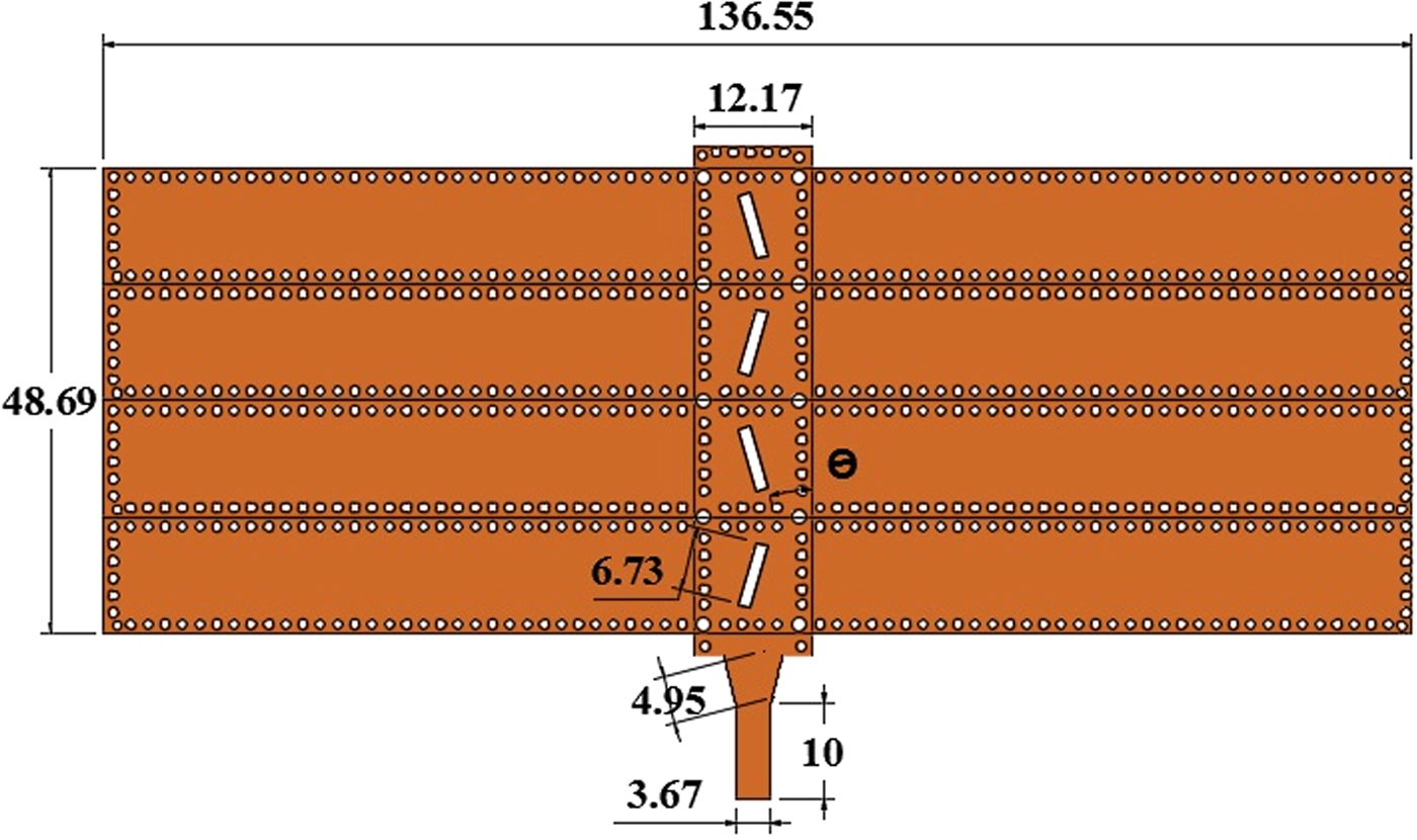
Fig. 4. Layout of the proposed double-layer aperture-coupled SIW antenna array.

Fig. 5. Simulation results for the aperture-coupled antenna with different θ angles. (a) E-plane field. (b) Gain.
Experimental results and discussion
The simulation and measurement results are provided under this section to demonstrate the performance of the aperture-coupled slotted SIW antenna. The proposed antennas are fabricated on a low-cost RO4003 substrate as shown in Fig. 6. The metal thickness of the PCB is considered as 18 μm. The requirements for adequate parallel screw placement, such as exact indication of distance and screw trajectory, were the primary factors in the construction of this aperture-coupled antenna. The Agilent E8361C PNA microwave network analyzer is used to measure the antenna reflection coefficient. The radiation patterns are measured in an anechoic chamber.

Fig. 6. Photograph of the proposed SIW slotted array antenna. (a) Inset feed design. (b) Aperture-coupled design.
Figure. 7 shows the comparison between the measured and simulated reflection coefficient as well as the normalized E-plane radiation pattern for the inset fed slot antenna. The measured SLL is below −12 dB in E-Plane with a little discrepancy by its simulated one (−13 dB) due to fabrication tolerances and measurement errors. The differences between the simulated and measurement results are due to ignoring the coaxial cable and the antenna holders used during the simulation procedure. The measured results propose a 6.8% impedance bandwidth for the inset feed design. The S 11 parameter as a function of frequency for different θ angles and normalized E-plane field plots for aperture-coupled feed network are provided in Fig. 8 for both simulation and fabricated results with θ = 15°. It is evident that there is a good agreement between the simulation results and measurement results with a little deviation due to fabrication tolerances and measurement errors. As depicted in Fig. 6, the SMA connector made an unbalanced geometrical configuration in the inset fed array antenna. This leads to an asymmetrical radiation pattern over the frequency band. The aforementioned drawback does not exist in the aperture-coupled feed system because of the symmetrical excitation of waveguide channels from the center point. The aperture-coupled SIW array antenna made higher robustness in the realized gain over the frequency band. The simulated group delay of the array antenna is relatively flat in the pass band and varies between 1 ns ~ 2.7 ns. It means the variation in the phase response is negligible for this antenna and it can transmit/receive high data rate pulse without distortion. An SLL near −13 dB has been achieved with a gain about 14 dB, validating the design procedure proposed in this paper.

Fig. 7. Comparison between the simulated and measured results of the planar inset feed SIW antenna. (a) S 11. (b) Normalized E-plane radiation pattern at 11.5 GHz.

Fig. 8. Comparison between the simulated and measured results of the aperture-coupled SIW antenna. (a) S 11. (b) Normalized E-plane radiation pattern at 11.5 GHz.
Conclusion
This paper presented two SIW slot antennas fabricated on the low-cost RO4003 microstrip board. The first design proposed an inset fed array network, however, the second one presented an aperture-coupled feed system to excite the SIW channels. The offset from the center line was chosen equal to have a uniform distribution of the radiators. This led to an SLL of −13 dB in the radiation pattern at 11.5 GHz. Non-uniform displacement of the slots should be applied to obtain lower SLLs. The proposed antennas, can be fabricated entirely by PCB process making them to be low-cost and easy to fabricate. The SMA connector made an unbalanced geometrical configuration in the inset fed design led to an asymmetrical radiation pattern over the frequency band. The aperture-coupled feed design led to overcome this drawback because of symmetrical excitation the waveguide channels from the center point. A comparative study of other types of compact SIW mono-pulse antennas shows that the proposed arrays provided good impedance matching and reasonable radiation patterns.
 J. Soleiman Meiguni received his M.Sc. and Ph.D. in electrical engineering from K. N. Toosi University of Technology, Tehran, Iran, in 2008 and 2013, respectively. In 2013, he joined the Faculty of Electrical and Computer Engineering, Semnan University of Iran as an assistant professor where he had been involved in department and group level service activities. In September 2017, he joined EMC-laboratory at Missouri University of Science and Technology, Rolla, MO, USA, as a visiting assistant research professor. He has authored and co-authored several papers in peer-reviewed journals and conference proceedings. His research is mainly focused on the areas of antennas, computational EM modeling, RF/Microwave, EMI/EMC for a different range of applications.
 S. Keshavarz Haddad was born in Tehran, Iran, on December 17, 1989. He received his B.Sc. from K. N. Toosi University of Technology, Tehran, Iran, in 2014 and his M.Sc. from Semnan University, Semnan, Iran, all in electrical engineering. He has participated in many projects inside and outside the university. His research area is planar antenna design, planar filter design, and millimeter-wave circuit design.
 A. Hosseinbeig received the B.S. degree in electrical engineering from Shahid Bahonar University, Kerman, Iran and M.S. and Ph.D. degrees in electrical engineering from K.N. Toosi University of Technology, Tehran, Iran in 2006, 2008, and 2013, respectively. He was an assistant professor at Islamic Azad University-Science and Research Branch, Tehran, Iran until 2016. From February 2016 to November 2017, he was a visiting assistant research professor with the EMC-laboratory at Missouri University of Science and Technology, Rolla, MO, USA. He is currently an EMC design engineer at Apple Inc., Cupertino, CA, USA. His current research interests include computational electromagnetics, system-level ESD, numerical, and measurement techniques related to ESD/EMC in electronic devices.


