


I. INTRODUCTION
Optoelectronic oscillator (OEO) was first proposed by M Nakazawa, T Nakashima, and M Tokuda [Reference Nakazawa, Nakashima and Tokuda1] in 1984 the journey of Optoelectronic oscillator (OEO) in shown in Fig. 1. The configuration of an OEO is similar to that of the van der Pol oscillator. In the van der Pol oscillator, the flux of electrons from the cathode to the anode is controlled by the potential on the inverting grid and thus this potential is affected by the feedback current in the anode circuit comprising a tuned circuit Fig. 2.

Fig. 1. Journey to OEO.
A van der Pol oscillator can be converted to an OEO by replacing the function of electrons by photons, the function of the grid by an electrical–optical (E/O) converter, the function of the anode by an optical–electrical (O/E) converter, and finally the energy-storage function of the LC circuit by a long optical delay line.
The structure of the Laser Induced Microwave Oscillator (LIMO) is described in Fig. 2. Here, light from an E/O modulator is detected by a photo detector after passing through a long optical delay line which is then amplified and fed back to the electrical port of the E/O modulator. If the modulator is properly biased and the small signal loop gain is larger than unity, self-sustained oscillations are achieved [Reference Yao and Maleki2–Reference Zhou and Blasche7]. The optical output of the intensity modulator is then passed down a long optical fiber delay line and into a photodiode. The recovered electrical signal is amplified and passed through an electronic bandpass filter. The output of the filter is then connected to the RF input of intensity modulator in order to complete the optoelectronic cavity. The electronic bandpass filter selects the frequency of oscillation by attenuating the other free-running modes below threshold [Reference Yao and Maleki2–Reference Yao and Maleki5]. The use of the very low loss optical fiber delay line is to create a cavity with a very high Q factor. The Q factor can be defined as the ratio of the stored energy in the cavity over the loss of the cavity. Since the loss of the fiber delay line is on the order 0.2 dB/km, a very long fiber can store a large amount of energy with very little loss. Because of this the Q factor of the OEO can easily achieve the level of 106 or higher. Yao and Maleki [Reference Yao and Maleki6] have developed a quasi-linear theory for the threshold condition, the amplitude, the frequency, the line width, and the spectral power density of the oscillation in OEO. The long delay line used in the oscillator can, however, support many modes of oscillation. Mode spacing is inversely proportional to the delay length of the optical link. The oscillator Q can be improved by increasing the delay length at the expense of tighter mode spacing. The undesirable modes become more difficult to filter in the RF domain as the spacing becomes closer [Reference Zhou and Blasche7–Reference Nguimdo, Chembo, Colet and Larger11]. The stability analysis of LIMO has been studied using Barkhausen criteria by Biswas et al. [Reference Biswas, Chatterjee and Pal12]. The effect of interfering signal on a synchronized oscillator has been studied in detail by earlier workers [Reference Biswas13–Reference Ray, Pramanik, Banerjee and Biswas15]. The contribution of phase noise in a multi-loop OEO has been investigated [Reference Eliyahu and Maleki16] and the movement of poles in OEO has been analyzed by Chatterjee et al. [Reference Chatterjee, Pal and Biswas17].

Fig. 2. Optoelectronic oscillator with interference.
As the technology has advanced, OEOs have been demonstrated to generate RF signals at frequencies starting in the microwave range and extending out to the millimeter wave range. Work continues on improving the performance of the original OEO, from using multiple loops to suppress the non-oscillating side modes by removing the bandpass filter in order to tune the frequency of RF output [Reference Yao18, Reference Maxin, Pillet, Steinhausser, Morvan, Llopis and Dolfi19]. Further work has been done on improving the phase noise performance by removing the electronic amplifier from the cavity while also looking at miniaturizing the OEO for use in satellites and computers. In terms of digital optical networks, the OEO has been used for both data clock recovery as well as data format conversion. Demonstrations of the OEO continue to explore new applications, from generating broadband chaos [Reference Callan20], use in sensors [Reference Duy21], performance evaluation utilizing photonic crystal fiber and standard fibers as delay lines [Reference Daryoush22], and as a measurement of the refractive index of optical fibers [Reference Gunn23].
If a sinusoidal signal acts on a nearly sinusoidal oscillator then the behavior of the oscillator affects in many aspects depending on the strength and frequency of the forcing signal. A forcing signal when injected into an oscillator modifies its properties in many ways. Within the synchronization range the locked oscillator loses its identity and obeys command from the forcing signal, and the oscillator is said to be injection locked (phase locked) to the synchronization signal [Reference Biswas, Chatterjee and Pal12–Reference Ray, Pramanik, Banerjee and Biswas15]. It is to be noted that the forcing signal can be injected into the OEO as an electrical or optical synchronizing signal. However, for the present study, we have considered the forcing synchronizing signal to be in the electrical form.
In this paper, we have derived an expression for the locking-range of an OEO under the influence of weak interference. We also show the variation of locking-range with injection amplitude. Finally, the effect of frequency-pulling and pushing on locking-range is also observed when the interference is swept away from the OEO's center frequency.
II. SYSTEM EQUATION OF OEO IN PRESENCE OF INTERFERENCE
Let the RF input to the modulating grid of the Mach–Zehnder modulator (MZM) is given by
 $$v_{in} \lpar t\rpar = V\lpar t\rpar e^{j\lsqb \omega_1 t + \theta \lpar t\rpar \rsqb }\semicolon \;$$
the synchronizing signal to be S(t) = Ee jω1 t and the interfering tone to be I(t) = yEe jω i t , where “ω i ” is the interfering frequency which is lying away from the OEO's free-running frequency, “y” is the fraction which indicates the strength of the interfering tone with respect to synchronizing signal, and “Δω = ω1 − ω i ” is the de-tuning frequency. If “G(s)” is the transfer function of the RF tuned circuit, then it can be expressed as [Reference Gonorovsky14] 1/G(s) = 1 + Q((s/ω0) + (ω0/s)), where “Q” is the quality factor of the tank circuit.
To analyze the behavior of the OEO in presence of the interfering signal shown in Fig. 2, we will assume that the OEO, instead of being exposed simultaneously to both the synchronizing signal and the interfering tone, is initially locked to the synchronizing signal and then it is influenced by the interfering tone which does not throw the system out of synchronism. In this condition, the instantaneous phase of the OEO will fluctuate around the static phase error “θ 1” at a rate depending upon the difference of frequencies between the synchronizing signal and the interfering tone. Similarly, the amplitude of the forced oscillator will also vary around the steady state value at a rate depending upon the frequency difference between the two signals. The static phase error “θ 1” gives a measure of the initial detuning of the OEO with respect to the synchronizing signal [Reference Ray, Pramanik, Banerjee and Biswas15].
Now, in order to find the system equation of the OEO in presence of interference we assume that despite the presence of strong non-linearity of MZM, there exists stationary amplitude of the microwave oscillation [Reference Biswas, Chatterjee and Pal12] of the form
 $$v_{in} \lpar t\rpar =V\lpar t\rpar \exp \lpar j\omega t + \theta \lpar t\rpar \rpar.$$
The output power [Reference Zhou and Blasche7, Reference Chatterjee, Pal and Biswas17] of the MZM can be expressed as
 $$P\lpar t\rpar = \displaystyle{1 \over 2} \alpha P_0 \left[1 - \eta \sin \left(\displaystyle{v_{in} \lpar t\rpar + V_B \over V_\pi} \right)\right]\semicolon \;$$
where “α” is the fraction of insertion loss of the modulator, “V π ” is the half-wave voltage, “V B ” is the bias voltage, “P 0” is the input optical power, “v in (t)” is the input RF voltage to the modulator and, “η” determines the extinction ratio of the modulator. Therefore, the output voltage of the photo detector when the output of the MZ modulator shines on it is
 $$\eqalign{V_0 \left(t \right)&= \rho Z_{ph} P\left(t - \tau \right)\cr &= \rho \sqrt{R^2 + \displaystyle{1 \over \omega ^2 C^2}} P\left(t - \tau \right)e^{ - j\tan^{ - 1} \left(\displaystyle{1 \over \omega CR} \right)} \cr & \cong \rho RP\left(t - \tau \right)e^{\displaystyle{1 \over \,j\omega \tau_1}}\semicolon \; }$$
where “ρ” is the sensitivity, “Z ph = R − (j/ω C)” is the output impedance of the photo-detector and “τ1 = RC” is the time-constant of photo-detector. Hence using the above arguments, it is not difficult to show that the output of the MZM [Reference Biswas, Chatterjee and Pal12] can be expressed as
 $$\eqalign{V_0 \lpar t\rpar & =- 2\eta V_{ph} \cos \left(\displaystyle{\pi V_B \over V_\pi} \right)J_1 \left(\displaystyle{\pi V\lpar t - \tau \rpar \over V_\pi} \right)\cr &\quad \times \sin \left[\omega \lpar t - \tau \rpar \right]e^{\displaystyle{1 \over \,j\omega \tau_1}} \cr &= \displaystyle{N\lpar V\lpar t - \tau\rpar \rpar \over V} \exp \lpar \!-\! s\tau\rpar v_{in} \lpar t\rpar \exp \left(\displaystyle{1 \over s\tau_1} \right)}$$
where,
 $$\eqalign{&N\lpar V\lpar t - \tau \rpar \rpar = - 2\eta V_{ph} \cos \left(\displaystyle{\pi V_B \over V_\pi} \right)J_1 \left(\displaystyle{\pi V\lpar t - \tau \rpar \over V_\pi} \right)\, {\rm and} \cr &V_{ph} = \displaystyle{\rho R\alpha P_0 \over 2}.}$$
Thus, the closed-loop equation of the OEO in presence of injection is given by
 $$\eqalign{&\left[\displaystyle{N\lpar V\lpar t - \tau \rpar \rpar \over V} e^{ - s\tau } e^{\displaystyle{1 \over s\tau _1}} v_{in} \lpar t\rpar + Ee^{j\omega_1 t} + yEe^{j\omega _i t} \right]= \displaystyle{v_{in} \lpar t\rpar \over G.G\lpar s\rpar }.}$$
 $$\eqalign{&\left[\displaystyle{N\lpar V\lpar t - \tau \rpar \rpar \over V}e^{ - s\tau } e^{\displaystyle{1 \over s\tau_1}} + \displaystyle{E \over V}e^{- j\theta \lpar t\rpar} + \; y \displaystyle{E \over V} e^{ - j\lsqb \Delta \omega t + \theta \lpar t\rpar \rsqb} \right] v_{in} \lpar t\rpar \cr &\quad = \displaystyle{v_{in} \lpar t\rpar \over G.G\lpar s\rpar }.}$$
Again, the complex frequency can be written as [Reference Biswas, Chatterjee and Pal12]
 $$\left. \matrix{s = j\omega = \displaystyle{1 \over v_{in} \lpar t\rpar } \displaystyle{dv_{in} \lpar t\rpar \over dt} = \displaystyle{1 \over V\lpar t\rpar } \displaystyle{dV\lpar t\rpar \over dt} + j\left(\omega_1 + \displaystyle{d\theta \over dt} \right)\hfill \cr \displaystyle{1 \over j\omega} \cong \displaystyle{1 \over j\omega_1} + \displaystyle{1 \over \omega_1^2} \left(\displaystyle{1 \over V\lpar t\rpar } \displaystyle{dV\lpar t\rpar \over dt} + j\displaystyle{d\theta \over dt} \right)\hfill} \right\}.$$
Rewriting (2) with the help of (3)
 $$\eqalign{& N\lpar V\lpar t - \tau \rpar \rpar e^{ - j\omega _1 \tau} e^{\displaystyle{1 \over \,j\omega_1 \tau_1}} + Ee^{ - j\theta \lpar t\rpar } + yEe^{ - j\lsqb \Delta \omega t + \theta \lpar t\rpar \rsqb } \cr & = \left(\displaystyle{V \over G} \right) \left[1 + \displaystyle{Q \over V} \left(\displaystyle{1 \over \omega_0} + \displaystyle{\omega_0 \over \omega_1^2} \right) \displaystyle{dV \over dt} + \;jQ\left\{\left(\displaystyle{\omega_1 \over \omega_0} - \displaystyle{\omega_0 \over \omega_1} \right) \right. \right. \cr &\left.\left. + \left(\displaystyle{1 \over \omega_0} + \displaystyle{\omega_0 \over \omega_1^2} \right) \displaystyle{d\theta \over dt} \right\}\right].}$$
Under the assumption that V B = V π, η = 1, πV ph = V π and V π = π [Reference Biswas, Chatterjee and Pal12], we have N[V(t − τ)] = 2J 1 [V(t − τ)] and when ω1 ≈ ω0, the real part of equation (4) gives the amplitude equation as
 $$\eqalign{\displaystyle{dV \over dt} &= \left(\displaystyle{\omega_0 \over 2Q} \right) \left\{2GJ_1 \lsqb V\lpar t - \tau \rpar \rsqb \left\{\cos \lpar \omega_0 \tau \rpar + \displaystyle{\sin \lpar \omega_0 \tau \rpar \over \omega_0 \tau_1} \right\} - V \right\} \cr &\qquad + \left(\displaystyle{\omega_0 \over 2Q} \right) GE \lcub \cos \lpar \theta \rpar + y \cos \lpar \Delta \omega t + \theta \rpar \rcub.}$$
Similarly equating the imaginary part, the phase equation can be obtained as
 $$\eqalign{&2J_1 \lsqb V\lpar t - \tau \rpar \rsqb \left\{\sin \lpar \omega_1 \tau \rpar - \displaystyle{\cos \lpar \omega_1 \tau \rpar \over \omega_1 \tau_1} \right\} + E\lcub \sin \lpar \theta \lpar t\rpar \rpar \cr &\quad +y \sin \lpar \Delta \omega t+\theta \lpar t\rpar \rpar \rcub =- \left\{\displaystyle{QV \over G} \left[\left(\displaystyle{\omega_1 \over \omega_0} - \displaystyle{\omega_0 \over \omega_1} \right) \right. \right. \cr &\left. \left. \quad+ \left(\displaystyle{1 \over \omega_0} + \displaystyle{\omega_0 \over \omega_1^2} \right) \displaystyle{d\theta \over dt} \right] \right\}.}$$
Again for ω1 ≈ ω0, the phase balance equation can be rewritten as
 $$\eqalign{& \displaystyle{d\theta \over dt} = \lpar \omega_0 - \omega_1\rpar - \left(\displaystyle{\omega_0 \over 2Q} \right)\left[\displaystyle{2GJ_1 \lsqb V\lpar t - \tau \rpar \rsqb \over V} \left\{\sin \lpar \omega _0 \tau \rpar \right. \right. \cr &\left. \left. \quad - \displaystyle{\cos \lpar \omega _0 \tau\rpar \over \omega_0 \tau_1} \right\} \right] - \left(\displaystyle{\omega_0 \over 2Q} \right)\left[\left(\displaystyle{GE \over V} \right)\lcub \sin \lpar \theta \lpar t\rpar \rpar \right. \cr &\left. \quad+ y\sin \lpar \Delta \omega t + \theta \lpar t\rpar \rpar \rcub \right].}$$
The photo-detector impedance “R” is replaced by “R − (j/ωC)” but it has no effect in our chosen frequency range. The effect of incorporating the photo-detector impedance in the amplitude and phase equations (5) and (7) has not been reported by other authors also.
III. WEAK INTERFERENCE LYING AWAY FROM THE OEO'S FREE-RUNNING FREQUENCY
Let us assume the solution for (6) as
 $$\theta = \theta_1 + m\sin \lpar \Delta \omega t + \alpha\rpar \comma \;$$
where “θ 1” is the steady-state phase error, and the modulation index is small for low-level interference. Using (8) in (7), we get
 $$\eqalign{& m\Delta \omega \cos \lpar \Delta \omega t + \alpha \rpar \cr &\quad = \lpar \omega_0 - \omega_1 \rpar - \left(\displaystyle{\omega_0 \over 2Q} \right) \left[\displaystyle{2GJ_1 [V\lpar t - \tau \rpar] \over V} \right. \cr &\left. \quad \left\{\sin \lpar \omega_0 \tau\rpar - \displaystyle{\cos \lpar \omega_0 \tau \rpar \over \omega_0 \tau_1} \right\} \right] - \left(\displaystyle{\omega_0 \over 2Q} \right) \left(\displaystyle{GE \over V} \right)\cr &\quad \times \left[\matrix{J_0 \lpar m\rpar \sin \theta _1 + 2J_1 \lpar m\rpar \cos \theta _1 \sin \lpar \Delta \omega t + \alpha \rpar \hfill \cr + \;yJ_0 \lpar m\rpar [\sin \theta_1 \cos \lpar \Delta \omega t\rpar + \cos \theta_1 \sin \lpar \Delta \omega t\rpar ] \hfill \cr + \;yJ_1 \lpar m\rpar [\cos \theta_1 \sin \alpha - \cos \alpha \sin \theta_1 ]\hfill} \right].}$$
Using harmonic balance method [Reference Ray, Pramanik, Banerjee and Biswas15], we get
 $$\eqalign{&2Q\left(\displaystyle{\omega_1 - \omega _0 \over \omega _0} \right)= \Omega \cr &\quad = - \left[\displaystyle{2GJ_1 [V\lpar t - \tau\rpar] \over V} \left\{\sin \lpar \omega_0 \tau \rpar - \displaystyle{\cos \lpar \omega_0 \tau\rpar \over \omega_0 \tau_1} \right\}\right]\cr & \quad - \left(\displaystyle{GE \over V} \right)\left[J_0 \left(m \right)\sin \theta_1 + yJ_1 \left(m \right)\sin \lpar \alpha - \theta_1\rpar \right].}$$
Similarly, denoting
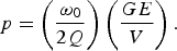 $p = \left(\displaystyle{\omega_0 \over 2Q} \right)\left(\displaystyle{GE \over V} \right).$
 $$\displaystyle{m\Delta \omega \over p} \cos \alpha = - \left[2J_1 \lpar m\rpar \cos \theta_1 \sin \alpha + yJ_0 \lpar m\rpar \sin \theta_1 \right]\comma \;$$
and
 $$\displaystyle{m\Delta \omega \over p}\sin \alpha = 2J_1 \lpar m\rpar \cos \theta_1 \cos \alpha + yJ_0 \lpar m\rpar \cos \theta_1.$$
Hence, it is not difficult to show using (11) that
 $$\sin \lpar \alpha - \theta _1 \rpar = \displaystyle{m\left(\Delta \omega \bigg{/}p \right) \over yJ_0 \lpar m\rpar}.$$
Substituting the value of (12) in (10)
 $$\eqalign{\Omega &=- \left[\displaystyle{2GJ_1 [V\lpar t - \tau \rpar] \over V} \left\{\sin \lpar \omega_0 \tau \rpar - \displaystyle{\cos \lpar \omega_0 \tau \rpar \over \omega_0 \tau_1} \right\} \right]\cr &\quad - \left(\displaystyle{GE \over V} \right) \left[J_0 \lpar m\rpar \sin \theta_1 + \left(\displaystyle{m\Delta \omega \over p} \right) \displaystyle{J_1 \lpar m\rpar \over J_0 \lpar m\rpar} \right].}$$
Again, using (11), it is not difficult to show that
 $$\eqalign{\Omega &= - \left[\displaystyle{2GJ_1 [V\lpar t - \tau \rpar] \over V} \left\{\sin \lpar \omega_0 \tau \rpar - \displaystyle{\cos \lpar \omega_0 \tau \rpar \over \omega_0 \tau_1} \right\}\right]- \left(\displaystyle{GE \over V} \right)\cr & \quad \times \left[J_0 \lpar m\rpar \sin \theta_1 + \displaystyle{m\left(\Delta \omega \bigg{/}p \right)y^2 J_0 \lpar m\rpar J_1 \lpar m\rpar \over m^2 \left(\Delta \omega \bigg{/}p \right)^2 + \;4J_1 ^2 \lpar m\rpar \cos ^2 \theta_1} \right].}$$
Now, for low-level interference, “m” is small and J 0(m) ≅ 1; J 1 (m) ≅ m/2. Maximum value of “θ 1” is ±(π/2). Hence from (14)
 $$\eqalign{\Omega & =- \left[\displaystyle{2GJ_1 [V (t - \tau)] \over V} \left\{\sin \lpar \omega _0 \tau \rpar - \displaystyle{\cos \lpar \omega _0 \tau \rpar \over \omega _0 \tau_1} \right\}\right]\cr &\quad - \left(\displaystyle{GE \over V} \right)\left[\sin \theta_1 + \left(\displaystyle{y^2 \over 2} \right)\displaystyle{\left(\Delta \omega \bigg{/}p \right)\over \left(\Delta \omega \bigg{/} p \right)^2 + \cos ^2 \theta_1} \right]\cr & =- \left[\displaystyle{2GJ_1 [V (t - \tau)] \over V} \left\{\sin \lpar \omega_0 \tau\rpar - \displaystyle{\cos \lpar \omega _0 \tau\rpar \over \omega_0 \tau_1} \right\}\right]\cr &\quad - \left(\displaystyle{GE \over V} \right)\left[\pm 1 + \displaystyle{y^2\bigg{/}2 \over \left(\Delta \omega \bigg{/}p \right)} \right].}$$
Now,
 $\displaystyle{y^2 \over 2} \displaystyle{p \over \Delta \omega}$
can be written as
$\displaystyle{y^2 \over 2} \displaystyle{p \over \Delta \omega}$
can be written as
 $\displaystyle{y^2 \over 2} \displaystyle{p \over \Delta \omega} = \Delta \omega - \sqrt{\lpar \Delta \omega \rpar ^2 - y^2 p}$
. Thus, the lock-range of the OEO in presence of the interfering tone is given by
$\displaystyle{y^2 \over 2} \displaystyle{p \over \Delta \omega} = \Delta \omega - \sqrt{\lpar \Delta \omega \rpar ^2 - y^2 p}$
. Thus, the lock-range of the OEO in presence of the interfering tone is given by
 $$\eqalign{\Omega &= - \left[\displaystyle{2GJ_1 [V (t - \tau)] \over V} \left\{\sin \lpar \omega _0 \tau \rpar - \displaystyle{\cos \lpar \omega _0 \tau\rpar \over \omega_0 \tau _1} \right\}\right]\cr &\quad - \left(\displaystyle{GE \over V} \right)\left[1 + \left(\Delta \omega - \sqrt{\lpar \Delta \omega \rpar ^2 - y^2 p} \right)\right].}$$
In deriving the steady-state value for the lock range given by equation (16), the positive sign of (15) has been considered. Moreover, since “V(t) and θ(t)” are slowly varying functions of time [Reference Gonorovsky14], i.e.
 $\displaystyle{1 \over \omega_0} \left(\displaystyle{d\theta \over dt} \right)\ll 1$
and
$\displaystyle{1 \over \omega_0} \left(\displaystyle{d\theta \over dt} \right)\ll 1$
and
 $\displaystyle{1 \over V}\left(\displaystyle{dV \over dt} \right)\ll 1$
,
$\displaystyle{1 \over V}\left(\displaystyle{dV \over dt} \right)\ll 1$
,
 $$V\lpar t - \tau \rpar \approx V\lpar t\rpar - \tau \displaystyle{dV \over dt} \approx V\lpar t\rpar \left[1 - \displaystyle{\tau \over V} \displaystyle{dV \over dt} \right]\approx V\lpar t\rpar \comma \;$$
and thus in the steady state
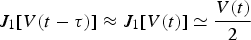 $J_1 [V (t - \tau)] \approx J_1 [V (t)] \simeq \displaystyle{V\lpar t\rpar \over 2}$
.
$J_1 [V (t - \tau)] \approx J_1 [V (t)] \simeq \displaystyle{V\lpar t\rpar \over 2}$
.
From (15), it is clear that in absence of interference
 $$\left. \Omega \right\vert_{Lower} = - \left[\displaystyle{2GJ_1 [V (t - \tau)] \over V} \sin \lpar \omega _0 \tau \rpar \right] - \left. \left(\displaystyle{GE \over V} \right) \right\vert_{\theta _1 = + {\pi \over 2}}.$$
 $$\left. \Omega \right\vert _{Upper}=- \left[\displaystyle{2GJ_1 \lsqb V\lpar t - \tau \rpar \rsqb \over V} \sin \lpar \omega_0 \tau \rpar \right] + \left. \left(\displaystyle{GE \over V} \right) \right\vert_{\theta_1 = - {\pi \over 2}}.$$
Hence Ω Lower > Ω Upper , which is also confirmed from the experimental findings given in Table 1 and Fig. 8. This asymmetric nature of the locking range of an OEO has not been reported so far as far as the knowledge of the authors goes.

Fig. 3. Locking range of injection-synchronized OEO with frequency detuning.
Table 1. Locking range with fiber delay.

Laser frequency = 500 Mrad/s; free-running frequency = 12.002 MHz; RF gain = 3; synchronizing signal strength = 0.4 V; interfering signal strength = 0 V.
IV. RESPONSE OF OEO TO NOISY SIGNAL
Thermal noise is the unavoidable form of interference that affects the behavior of the closed-loop system shown in Fig. 4. The power spectral density of the thermal noise is flat, frequency independent and hence the name white noise. It is expedient to write the signal contaminated with additive white Gaussian noise while passing through the narrow-band tuned circuit in absence of interfering tone as
 $$\eqalign{&v_n \left(t \right)= \sqrt 2\, V_C \left(t \right)\cos \left[{\omega _1 t+\theta \left(t \right)} \right]+\sqrt 2\, V_S \left(t \right)\sin \left[{\omega _1 t+\theta \left(t \right)} \right]\cr &\quad\quad =\sqrt {2\left[{V_C ^2 \left(t \right)+V_S ^2 \left(t \right)} \right]} e^{\,j\left[{\omega _1 t+\theta \left(t \right)- \theta _n \left(t \right)} \right]}\comma \; }$$
where “
 $V_C \lpar t\rpar $
” and “
$V_C \lpar t\rpar $
” and “
 $V_S \lpar t\rpar $
” are the narrowband independent Gaussian variables with one-sided power spectral density “N
0”. The closed loop equation in this case will be
$V_S \lpar t\rpar $
” are the narrowband independent Gaussian variables with one-sided power spectral density “N
0”. The closed loop equation in this case will be
 $$\eqalign{&\left[\displaystyle{N\lpar V\lpar t - \tau \rpar \rpar \over V\left(t \right)} e^{ - s\tau} v_{in} \lpar t\rpar + Ee^{j\lsqb \omega _1 t + \psi \lpar t\rpar \rsqb } \right. \cr &\quad \left. +\sqrt{2\left[V_C ^2 \lpar t\rpar +V_S ^2 \lpar t\rpar \right]} e^{j\lsqb \omega_1 t + \theta \lpar t\rpar - \theta _n \lpar t\rpar \rsqb } \right]= \displaystyle{v_{in} \lpar t\rpar \over G.G\lpar s\rpar }. \cr &\displaystyle{N\lsqb V\lpar t - \tau \rpar \rsqb \over V\lpar t\rpar } e^{ - s\tau } v_{in} \lpar t\rpar + \displaystyle{E \over V\lpar t\rpar } e^{j\phi \lpar t\rpar } v_{in} \lpar t\rpar \cr &\quad + \sqrt{2} \displaystyle{V_n \lpar t\rpar \over V\lpar t\rpar } e^{ - j\theta _n \lpar t\rpar } v_{in} \lpar t\rpar = \displaystyle{v_{in} \lpar t\rpar \over G.G\lpar s\rpar }.}$$
Following similar analysis, the amplitude and phase equations are given by
 $$\eqalign{&\displaystyle{dV \over dt} = \left(\displaystyle{\omega_0 \over 2Q} \right) \left\{2GJ_1 \lsqb V\lpar t - \tau \rpar \rsqb \cos \lpar \omega_0 \tau \rpar - V\lpar t\rpar \right\} + \left(\displaystyle{\omega_0 \over 2Q} \right)\cr &\qquad \times \left\{\displaystyle{GE \over V\lpar t\rpar} \cos \lsqb \phi \lpar t\rpar \rsqb + \sqrt{2} G\displaystyle{V_n \lpar t\rpar \over V\lpar t\rpar} \cos \lsqb \theta _n \lpar t\rpar \rsqb \right\}\comma \;}$$
and
 $$\eqalign{& \displaystyle{d\phi \over dt} = \displaystyle{d\psi \over dt} - \displaystyle{d\theta \over dt} \cr &=\left[\Delta \omega + \omega _m K_p \cos \lpar \omega _m t\rpar \right]+ \left(\displaystyle{\omega_0 \over 2Q} \right)\cr &\quad \times \left\{2G\displaystyle{J_1 \lsqb V\lpar t - \tau \rpar \rsqb \over V\lpar t\rpar } \sin \lpar \omega _0 \tau \rpar \right\} - \left(\displaystyle{\omega_0 \over 2Q} \right)\displaystyle{GE \over V\lpar t\rpar } \sin \lsqb \phi \lpar t\rpar \rsqb \cr & \quad+ \left(\displaystyle{\omega_0 \over 2Q} \right)\sqrt{2} G\displaystyle{V_n \lpar t\rpar \over V\lpar t\rpar } \sin \lsqb \theta _n \lpar t\rpar \rsqb.}$$
where
 $V_n \lpar t\rpar =\sqrt {V_C ^2 \lpar t\rpar +V_S ^2 \lpar t\rpar } $
and
$V_n \lpar t\rpar =\sqrt {V_C ^2 \lpar t\rpar +V_S ^2 \lpar t\rpar } $
and
 $\theta _n \lpar t\rpar =\tan ^{ - 1} \left[{\displaystyle{{V_S \lpar t\rpar \over V_C \lpar t\rpar }}} \right]$
. Choosing
$\theta _n \lpar t\rpar =\tan ^{ - 1} \left[{\displaystyle{{V_S \lpar t\rpar \over V_C \lpar t\rpar }}} \right]$
. Choosing
 $\beta=\left({\displaystyle{{\omega _0 / 2QV_0 }}} \right)$
, we start with the assumption that the oscillator is in the locked state under the influence of the signal. Assuming an initial detuning, it is not hard to conjecture that the instantaneous phase error will consist of three terms, viz., (1) a dc component due to initial detuning, (2) a component at the modulating frequency, and (3) random fluctuations due to noise. As a result, the solution of (21) may be assumed to be of the form
$\beta=\left({\displaystyle{{\omega _0 / 2QV_0 }}} \right)$
, we start with the assumption that the oscillator is in the locked state under the influence of the signal. Assuming an initial detuning, it is not hard to conjecture that the instantaneous phase error will consist of three terms, viz., (1) a dc component due to initial detuning, (2) a component at the modulating frequency, and (3) random fluctuations due to noise. As a result, the solution of (21) may be assumed to be of the form
 $$\phi=\phi _0+M\sin \lpar \omega _m t+\delta \rpar +\phi _n \lpar t\rpar \comma \;$$
where “ϕ
n
(t)” is a zero mean random variable due to the incoming noise and it is to be remembered that the random variable “ϕ
n
” has a variance “σϕ
Reference Yao and Maleki
2
”. It is to be noted also that “ϕ
n
” is not truly Gaussian but if the input carrier-to-noise ratio is not very small, the probability density function of “ϕ
n
” approximates closely to that of a Gaussian variable, i.e.
 $p\lpar \phi _n \rpar = \displaystyle{1 \over \sigma_\phi \sqrt{2\pi}} e^{ - \left({\phi_n^2 \over 2\sigma_\phi^2} \right)}$
. It is not difficult to show using (21), (22) and statistical linearization techniques
$p\lpar \phi _n \rpar = \displaystyle{1 \over \sigma_\phi \sqrt{2\pi}} e^{ - \left({\phi_n^2 \over 2\sigma_\phi^2} \right)}$
. It is not difficult to show using (21), (22) and statistical linearization techniques
 $$\eqalign{& \displaystyle{d\phi _0 \over dt} + M\omega_m \cos \lpar \omega _m t + \delta \rpar +\displaystyle{d\phi _n \over dt} \cr & = \left[\Delta \omega + \omega _m K_p \cos \omega _m t \right]+ \left(\displaystyle{\omega_0 \over 2Q} \right)GC\sin \lpar \omega_0 \tau\rpar + \beta GN_2 \lpar t\rpar \cr & \quad - \beta GE\left[\left\{e^{ - ^{{\sigma_\phi^2 \over 2}}} \sin \phi _0+\phi _n e^{ - ^{{\sigma_\phi^2 \over 2}}} \cos \phi_0 \right\}J_0 \lpar M\rpar \right. \cr &\quad \left. +2J_1 \lpar M\rpar \sin \lpar \omega _m t+\delta \rpar \left\{e^{ - ^{{\sigma_\phi^2 \over 2}}} \cos \phi_0 + \phi _n e^{ - ^{{\sigma_\phi ^2 \over 2}}} \sin \phi_0 \right\}\right]\comma \; }$$
where,
 $N_2 \lpar t\rpar =\sqrt 2\, V_n \lpar t\rpar \sin \lsqb \theta _n \lpar t\rpar \rsqb $
and
$N_2 \lpar t\rpar =\sqrt 2\, V_n \lpar t\rpar \sin \lsqb \theta _n \lpar t\rpar \rsqb $
and
 $\left. \phi_0 \right]_{\max } = \pm \left(\displaystyle{\pi \over 2} - M - \sigma _\phi \right)$
; “±” sign refers to the upper or lower side locking ranges for the OEO. Hence, the variance of the phase error is given by
$\left. \phi_0 \right]_{\max } = \pm \left(\displaystyle{\pi \over 2} - M - \sigma _\phi \right)$
; “±” sign refers to the upper or lower side locking ranges for the OEO. Hence, the variance of the phase error is given by
 $$\eqalign{\sigma_\phi ^2 &= \lpar \beta G\rpar ^2 \displaystyle{N_0 \over 2} \vint_{ - \infty}^{\infty} \left\vert \displaystyle{1 \over s + \beta GEJ_0 \lpar M\rpar e^{{ - \sigma_\phi^2 \over 2}} \cos \lpar \phi _0\rpar } \right\vert^2 ds \cr &= \displaystyle{\pi \beta GN_0 \over 2E} \times \displaystyle{1 \over J_0 \lpar M\rpar e^{{ - \sigma_\phi^2 \over 2}} \sin \lpar M - \sigma _\phi \rpar }\comma \;}$$
where, “N 0 = kT”, “k” is the Boltzmann's constant and “T” is the noise temperature.

Fig. 4. Experimental set-up for the study of locking range.
V. RESULTS AND DISCUSSIONS
Theoretical variation of lock range with frequency detuning of the OEO has been shown in Fig. 6, using MATHCAD 14.0 software. It clearly indicates that with frequency detuning (Δω), the lock range increases. Experimental results which are given in Table 2 and Fig. 6 agree well with that obtained theoretically. However, for our experimental set-up, we have chosen the fiber delay to be 10 µs on the RF signal carried by the optical signal. This corresponds to a 100 kHz mode spacing such that the next optical mode is situated at 12.102 MHz, shown in Fig. 7. It is to be noted that the free-running frequency of the OEO is 12.002 MHz. Hence, as the interference is swept away from the center frequency of the OEO, frequency pulling affect by the neighboring side band is observed, which will eventually decrease the lock range. Thus it is expedient to keep the frequency detuning low, hence avoiding the frequency pulling by the neighboring side bands of the OEO. In Fig. 5, the variation of locking range with injection amplitude has been studied (Table 3). The graph shows the variation of locking range with and without interfering signal. Asymmetry in locking range is noticed from Table 1 and Fig. 8. This interesting observation is also evident from equations (17) and (18). Finally, we have shown the effect of Gaussian noise on the system performance and have given a method to calculate the variance of the phase error.

Fig. 5. Experimental variation of locking range with injection amplitude.

Fig. 6. Experimental variation of locking range with frequency detuning, “o – Experimental data”, “solid line – Data fit”.

Fig. 7. Locking range with fiber delay.

Fig. 8. Experimental variation of locking range with injection amplitude.
Table 2. Locking-range of injection synchronized OEO with interference.

Laser frequency: 500 Mrad/s, delay: 10.00 µs, interference amplitude = 0.09 V; free running frequency: 12.002 MHz; RF amplifier gain = 3.
Table 3. Locking-range variation with injection amplitude in OEO.

Laser frequency: 500 Mrad/s, delay: 10.00 µs, interference amplitude = 0.09 V; free running frequency: 12.002 MHz; RF amplifier gain = 3.
VI. CONCLUSION
In this paper, we have followed the same cyclic passage theory using Barkhausen's criteria as Biswas et al. [Reference Biswas, Chatterjee and Pal12]. A novel method of calculating the locking range of the synchronized oscillator in presence of interference has been presented. We have also reported an interesting phenomenon of the OEO, i.e. the locking range of the OEO in absence of interference is not symmetric. The variations of locking range with the frequency detuning, injection amplitude have been studied both theoretically and experimentally. The effect of photo-detector impedance have been incorporated in deriving the steady-state amplitude and phase equations, but no significant improvement is observed while replacing the photo-detector impedance “R” by “
 $R - \lpar j/\omega C\rpar $
” in our chosen frequency range. We have chosen the RF amplifier gain in such a way that the system is not over-driven or under-driven. Finally, we have studied the effect of additive-white Gaussian noise on OEO.
$R - \lpar j/\omega C\rpar $
” in our chosen frequency range. We have chosen the RF amplifier gain in such a way that the system is not over-driven or under-driven. Finally, we have studied the effect of additive-white Gaussian noise on OEO.
ACKNOWLEDGEMENT
Authors are thankful to the management of Sir J.C. Bose School of Engineering for carrying out the work at Sir J.C Bose Creativity Centre of Supreme Knowledge Foundation Group of Institutions, Mankundu, Hooghly.
 Arindum Mukherjee received the B. Tech. and M. Tech. in Optics and Optoelectronics, from University of Calcutta, in 2003 and 2005, respectively. At present, Mr. Mukherjee is working at Central Institute of Technology (A Centrally funded Institute under MHRD, Govt. of India), Assam, India. He is currently working toward the Ph.D. degree in “On some aspects of Remote Carrier Generation for Mobile Communication” with the Institute of Radio Physics and Electronics, University of Calcutta, India. His area of interests include optoelectronic oscillator, injection locked oscillator, phase locked loops, teager energy operator, etc.
 Somnath Chatterjee received his B. Sc. and M. Sc. degree in Physics from Burdwan University, West Bengal, India in the year 1998 and 2001, respectively. Currently, he submitted his Ph.D. thesis to West Bengal University of Technology. He received the URSI Young Scientist Award of the International Union of Radio Science in the year 2005 and has authored 16 international peer reviewed journal papers and attends various national and international conferences. At present, Mr. Chatterjee is with the Kanailal Vidyamandir (French Section), Chandernagore as a Headmaster/Principal. His area of interests include active microstrip patch and slot antenna; optoelectronic oscillator and injection locked oscillator etc. He has been the reviewer of several international journals.
 Nikhil Ranjan Das obtained his B. Tech. (1985), M. Tech. (1987) in Radio Physics and Electronics and the Ph.D. degree (1993) in the area of submicron structures of semiconductors, all from the University of Calcutta. He joined the Department of Radio Physics and Electronics in 1994, where he is currently a Professor. From September 1999 to July 2002, he was a Post-Doctoral Fellow and a Post Doctoral Research Associate (since 2001) with the Department of Electrical and Computer Engineering, McMaster University, Canada. Visiting Professor McMaster University (Canada), University of Sheffield (UK) and at Pohang University of Science and Technology (South Korea). His field of work includes semiconductor nanostructures, optoelectronic/photonic devices, nanophotonic detectors (MWIR/LWIR) and nano-bio sensors. Dr. Das is a Fellow of the IETE, Senior Member of IEEE, Life Member of the Indian Physical Society and the IACS. He has been the reviewer of several IEEE and other international journals.
 B. N. Biswas Emeritus Professor, Chairman, Education Division SKF Group of Institutions Former National Lecturer (UGC), Emeritus Fellow (AICTE), Visiting Faculty University of Minnesota (USA); Founder Prof-in-Charge University Institute of Technology, Microwave Division (BU); CU Gold Medalist; URSI Member: Commissions C, D, E and Developing Countries, Seminar Lecture tour to: University of Pisa (Italy), University of Bath (UK), University College (London), University of Leeds (UK), University of Kyoto (Japan), University of Okayama (Japan), Electro Communication University (Osaka), Czech Academy of Sciences; University of Erlangen (Germany), National Singapore University etc; Best Citizens Award (2005); Member: various National & Intl. Committees, Recipient of Various Awards. Supervised 23 Ph.D. students and being the author of 235 Publications in IEEEs and other referred journals.


