


I. INTRODUCTION
High speed internet access has become an increasingly important part in everyday life and a driving force for technological progress. Due to the lack of terrestrial coverage, high data rate services are not commonly available in remote areas or on board aircrafts. Wideband satellite services such as KA-SAT [Reference Eutelsat1] or Inmarsat 5 [2] at Ka-band offer well suited solutions from geostationary orbit. On the downside, relatively large high gain antennas are required for an adequate link budget, thus making a constant tracking of the narrow beam a necessity and challenge for mobile communications. Furthermore, satellite spotbeams employ orthogonal circular polarization to make use of the four-color-scheme [Reference Guy3]. For a mobile earth station, the used frequencies at Ka-band are 30 GHz for the uplink (T x ) and 20 GHz for the downlink (R x ). Mobile terminals for planes, ships, and ground vehicles have to meet these requirements while they also need to be flat and compact to meet customer demands. A planar array with electronic beam scanning could be a viable solution. Due to the very different frequencies, the transmit and receive arrays are often realized as separate units [Reference Kuhlmann, Rohrdantz and Jacob4, Reference Geise and Jacob5]. To minimize the total antenna size the transmitter and receiver arrays have to be merged into a single unit. Furthermore, a shared T x and R x aperture could be used to feed a reflector antenna in a so called focal plane configuration.
The construction of such a shared transmit and receive aperture with dual-polarized radiators is challenging. Indeed, to avoid grating lobes the array elements have to be spaced by less than half the freespace wavelength at the highest operating frequency. The resulting limited element size prevents using generally larger, wideband antennas. Furthermore, coupling between antenna feeds is a critical issue since it deteriorates the polarization properties. A wideband dual-polarized antenna has been proposed in [Reference Lee, Ahn and Chang6]. However, it is compatible with neither Ka-band services, nor standard printed circuit board (PCB) processes. Dual-polarized dual-band antennas have been reported for L- and X-Band [Reference Pozar and Targonski7] and recently as a concept for Ka-band [Reference Greco, Amendola, Arnieri, Boccia and Sandhu8]. In [Reference Smolders, Mestrom, Reniers and Geurts9] dipole antennas are used, which are not ideally suited when a large scanning range is required [Reference Kuhlmann and Jacob10]. For this reason, a dual-band and dual-polarized patch antenna at Ka-band has been developed and reported in [Reference Rohrdantz, Jaschke, Gellersen and Jacob11]. In this contribution further insight is provided in the design process and farfield measurement results are presented. Additionally, several arrays that are designed and realized using the dual-band patch antenna are reported.
This paper starts with a detailed description of the design process and the obtained custom patch antenna featuring dual-polarization and simultaneous 20 and 30 GHz operation in Section II. The design approach is explained, and the final layout of the realized antenna is presented. The achieved performance is assessed in Section III. Section IV is devoted to the arrays. Measurement results are presented and validate the taken approach.
II. DUAL-BAND AND DUAL-POLARIZED ANTENNA ELEMENT
The main design goal is to obtain a dual-band patch antenna that can be operated in 500 MHz bands at 20 GHz for downlink and 30 GHz for uplink. The antenna size must be smaller than half the freespace wavelength at 30 GHz to avoid grating lobes when used as array element. To enable spotbeam handover, the antenna must feature dual-polarization. Thus, a high return loss, a low axial ratio (AR), and well-shaped antenna patterns in the bands of interest are sought. Furthermore, a fabrication using a standard PCB process is intended.
The antenna makes use of a stacked patch and a crossed-feed structure. The final geometry is depicted in Fig. 1. It requires five metal layers: The two uppermost contain the antenna, the middle one a ground plane with an aperture, and the bottom two the feed lines to excite two orthogonal polarizations. The design procedure is explained in more detail in the following sections.

Fig. 1. Geometry of the dual-band patch antenna at Ka-band with two polarization ports.
A) Radiating element for dual-band operation
The design of a suitable radiating element is crucial for dual-frequency operation. Conventional microstrip patches exhibit a rather small fractional bandwidth of 5–20%. This is not enough for a wideband design ranging from 20 to 30 GHz. As a solution patch antennas can be employed, that use specifically designed shapes in combination with cutouts to influence the higher order transverse magnetic (TM)-modes for an adjustable dual-frequency behavior [Reference Lelaratne and Langley12, Reference Yang and Wong13]. To avoid a null in boresight direction, the excitation of the TM30-mode must be avoided. Often however, this is not possible, yields very narrow bandwidth, or results in geometries not realizable with the resolution available through standard PCB processes.
Thus, a stacked patch approach is taken [Reference Bafrooei and Shafai14]. The upper antenna is a square patch, which mainly influences the upper frequency band. A square-ring is placed in the layer below, yielding a second resonant frequency which is lower than of an equally sized conventional patch. The arrangement is depicted in Fig. 2(a). Overall, the element is smaller than 0.3λ 0,30 GHz, enabling the integration into an array with acceptable low inter-element coupling. The relatively thick antenna substrates ensure that the bandwidth requirements can be met.

Fig. 2. (a) Geometry of the stacked patch antenna. (b) Dependence of the resonant frequency and 10-dB bandwidth on antenna dimensions at the lower (—) and upper band (- -).
The stacked patches effectively function as a dual-band antenna, that radiates in both frequency bands. The fields are mainly concentrated between the ring and the ground plane in the lower band and between the upper patch and the lower ring/ground at the upper frequency. Changing the cutout thus affects both bands. In conclusion, the main three parameters to be adjusted are the lengths of the top patch, of the bottom square-ring, and of the cutout. Figure 2(b) illustrates how the resonant frequency and the 10-dB bandwidth are affected by changes Δl of these parameters. Changing the size of the top patch only influences the upper resonant frequency, while the lower resonance remains unchanged. The opposite applies for a change in size of the square-ring. Changing the cutout is more complex and the bandwidth of the resonance must be considered as well. A larger cutout reduces the lower resonant frequency and thus allows to reduce the antenna size. At the same time the bandwidth is decreased as the square-ring behaves more and more like a ring resonator. On the other hand the top patch can be excited more easily through the opening in the middle and its bandwidth increases. Thus, a compromise must be found for sufficient bandwidth and good matching in both bands.
B) Feed and aperture for dual polarization
The designed radiating element is symmetric and can thus support two linearly polarized modes. To excite both independently, two perpendicular feeds below an appropriate aperture are needed. Their placement is crucial to obtain a low return loss and low cross-coupling. Ideally both feed lines cross below the center of the aperture. Since this would result in an overlap they are conventionally placed closer to the patch edges, which results in higher cross-coupling [Reference Targonski and Pozar15] and an asymmetrical radiation pattern.
As a solution, the multilayer feed structure used in [Reference Lee, Ahn and Chang6] is adapted for the proposed dual-band antenna in a standard PCB process to meet the alignment challenges at higher frequencies. The feed lines traverse in the middle of a cross-shaped aperture and are only separated by a very thin layer. The ends of the feed are fanned out like a tuning fork to minimize blockage. The arrangement is illustrated in Fig. 3(a).

Fig. 3. (a) Illustration of the multilayer feed network with hourglass-shaped aperture. (b) Dependence of the magnitude of the input reflection coefficient at resonance on changes of the feed length at the lower (—) and upper band (- -).
The close proximity of the layer between the two feeds in combination with their shape yield quasi equal coupling of both feeds to the patch and adequate isolation. Length and width are adjusted for optimal matching in both frequency bands. This is illustrated in Fig. 3(b), where the feed length of the upper and the lower feed is varied by Δl. In this manner, it is possible to obtain equally good matching in both bands. An hourglass shaped aperture with two crossed slots (cf. Fig. 3(a)) is used to improve the return loss of the whole structure. A longer aperture improves the lower band, while it deteriorates the upper one and vice-versa. Furthermore, an adjustment of the minimal width of the hourglass shape in the center of the aperture can improve the matching. In this design the value is set to 0.08 mm, which is the limit imposed by the PCB process resolution.
C) Complete design and realization
The two stacked patches, the hourglass-shaped aperture and the crossed feed lines are combined in a five layer PCB-design to form the dual-band, dual-polarized antenna. The overall structure is optimized to obtain good matching in the desired Ka-band operating regime. The overall multilayer stack is illustrated in Fig. 4(a). For the most part it relies on the Rogers 4000 series [16] material system. To obtain a close spacing between the two feed layers 50 µm thin RO3850 Ultralam is used. Adjacent substrate cores are bonded with Rogers 4450F prepreg. Vias are required between the two lowest layers for the bottom feed and between ground plane and backside for the connector and the termination resistor at unused ports. Despite the five metal layers, this PCB design requires only one press cycle. This material stack-up is utilized for all built and simulated antennas in this paper.

Fig. 4. (a) Multilayer stackup. (b) Photograph of front and backside of the fabricated antenna.
An antenna was manufactured according to the introduced design. A photograph of the antenna top side is shown on the right-hand side of Fig. 4(b). The top patch is clearly visible while the ring beneath is barely recognizable through the top substrate layer. The bottom side with the feed network is depicted on the left-hand side of Fig. 4(b). Again, the second feed line on the adjacent layers beneath the cross-shaped aperture is only slightly visible through the substrate. A 2.92 mm connector can be attached for measurements.
III ANTENNA CHARACTERISTICS
A) Reflection coefficient
The input reflection coefficient of the complete antenna is shown in Fig. 5(a). Simulated and measured S-parameters are plotted for both the lower and the upper feed. The measured data was recorded with a network analyzer using a coplanar test fixture. Calibration was performed using a standard SOLT-procedure. Both operational bands can be clearly distinguished. The matching is better than 10 dB throughout the operational bands.

Fig. 5. (a) Simulated and measured reflection coefficients. (b) Simulated input reflection coefficient at port 1 and isolation between the two feed ports.
Only minor deviations between the two feeds are observed. At the upper band there is a slight frequency shift between the ports and the bandwidth is larger. Measurements and simulation are in good agreement and hence fully validate the concept. All simulations are carried out using a transient fullwave solver. The differences are mainly due to the test fixture transition that is not included in the calibration. Figure 5(b) shows the coupling between the ports. The low coupling of less than −15 dB minimizes the unwanted excitation of the orthogonal mode and thus the cross-polar polarization.
B) Radiation characteristics
To assess the patch radiation characteristics the antenna is simulated at 20 and 30 GHz on a finite 7 × 7 mm2 ground plane. Figure 6(a) shows the directivity at the lower band in three azimuthal cuts at φ = 0°, φ = 45°, and φ = 90°. For the simulation only port 1 is excited, while the other is terminated. Due to the similarity the results for the second port are omitted. The antenna features a very symmetric pattern in all three planes with only minor variances towards higher elevation angles. The maximal directivity reaches 6 dBi, while the 3-dB beamwidth is roughly ±45°, as expected from a patch antenna.

Fig. 6. Simulated radiation pattern (directivity) in three different azimuthal cutting planes at 20 GHz (a) and at 30 GHz (b).
At 30 GHz the results are similar, however, the directivity is slightly higher and the beamwidth is decreased (cf. Fig. 6(b)). Additionally, more asymmetries are observable at higher elevation angles.
Circular polarization is of major importance for Ka-band mobile satellite communications. To operate the proposed antenna in this fashion, the two antenna polarizations have to be excited with a 90° phase shift, which superimposes the two orthogonal linearly polarized modes to create a circular one. For dual-band operation this has to be achieved simultaneously in both bands, so that dual-band 3 dB quadrature couplers are required. These are not the scope of this paper, but solutions such as Lange couplers or microstrip couplers exist that could be integrated on the feed layers in the available space. To assess the performance, both ports are excited accordingly in simulation.
The frequency dependence of the AR is investigated in simulation. The results in boresight direction are reported in Fig. 7. The cross-coupling of roughly 20 dB between the two polarization ports precludes a lower AR.
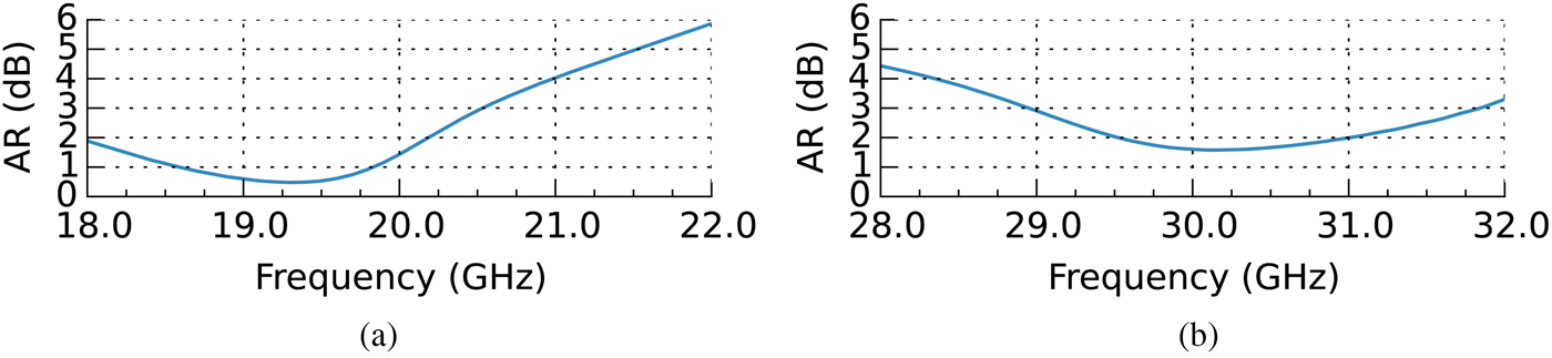
Fig. 7. Simulated frequency dependence of the AR in (a) the lower and (b) the upper band.
The angular characteristics of the AR are shown as contour plots in Fig. 8. The results at 20 GHz are depicted in Fig. 8(a). The AR remains below 6 dB in the whole upper hemisphere and is below 3 dB within ±60° in elevation.

Fig. 8. Simulated AR in the upper hemisphere at 20 GHz (a) and at 30 GHz (b).
In comparison with the lower band the circular polarization at 30 GHz is deteriorated, especially towards higher elevation angles θ. In the angular ranges ±45° and ±60° the AR remains below 3 and 6 dB, respectively. In an array application the rotation of neighboring array elements and a corresponding excitation (sequential rotation) can be employed to further improve these results [Reference Teshirogi, Tanaka and Chuju17].
IV. ANTENNA ARRAY
The intended application of the designed antenna is in satellite communications with geostationary satellites. For that purpose a single patch antenna has insufficient gain and an array of patch antennas is required. Since the overall size of the dual-band element is smaller than half the freespace wavelength at 30 GHz a rectangular array can be constructed without generating grating lobes in the visible range. However, due to the close proximity of the elements coupling effects between neighboring antennas may occur. This is investigated next after a detailed description of the array design procedure. Finally, measurement results are presented for two fixed beam arrays. The full-wave simulations in this section are carried out using accurate models of the manufactured circuits including the multilayer stack. A transient solver is used and all losses as well as surface roughness are included.
A) Array element performance
To evaluate the properties of a single antenna element embedded in an array, two small test arrays are manufactured. One of them is meant for a far field measurement of a single antenna whereas the second one is utilized to determine the coupling between neighboring elements. The latter consists of 16 antenna elements with the feed ports of the center four elements connected to microstrip lines. The surrounding 12 elements are terminated by microwave resistors (Vishay FC 50 Ω) to minimize parasitic reflections. The feed structure of the array on the backside of the antenna is depicted in Fig. 9(a). For the measurements, two microstrip lines are connected to a network analyzer, while the other ports are terminated. To get accurate results a TRL-calibration is performed on the antenna substrate.

Fig. 9. Array feed network configuration on the backside of the antennas for (a) S-parameter and (b) farfield measurements.
The measured isolation of the two polarization ports of one antenna (ports 1 and 2 from Fig. 9(a)) are summarized in Table 1. The table reports the value of minimal isolation in the upper and lower band (29–30.5 and 19–20.5 GHz, respectively) between the reference port and all other seven ports. A full-wave simulation using the same setup but with ideal 50 Ω resistors is carried out. The obtained results are also listed in Table 1 and validate the measured results.
Table 1. Minimal measured and (simulated) isolation (in dB) between one antenna port and all neighboring elements in the array in the low and high band.

It can be observed that the isolation is generally higher than 20 dB and better in the upper band. Because of the symmetric arrangement the isolation of the other three antennas is similar and thus omitted in the table. Generally, all cross-polarized ports are well decoupled with the exception of the second antenna feed port. The highest coupling of −11 dB is observed for neighboring elements of the same polarization that use a lower feed and occurs in the H-plane (e.g. between element 1–4 and 2–7). The main coupling is caused by the feed network and not by the patches. Simulation shows, that the isolation between adjacent antennas can be significantly improved to about 25 dB by introducing ground vias between neighboring feeds. The measured coupling of −15 dB between ports 1 and 2 is in good agreement with the simulation results from Fig. 5(b) and indicates that the single antenna performance is not significantly affected in an array setup.
To conduct the far field measurements a single antenna element in an array setup with surrounding elements is used (c.f. Fig. 9(b)). The outer elements are terminated with 50 Ω resistors, while the two polarization ports of the center element remain accessible for the measurements. The far field measurement is conducted in an anechoic environment with the antenna mounted on a rotatable positioner. The setup can be seen in Fig. 10 with a different 4 × 4 array mounted on the positioner. A horn antenna serves as reference during the co- and the crosspolar E- and H-plane measurements. A low noise amplifier helps to improve the dynamic range of the power meter at the receiver. The measured data is evaluated by means of a transmission model containing the freespace loss, cable losses, amplifier gain, and a model of the reference antenna obtained experimentally (three-antenna-method).

Fig. 10. Measurement setup in an anechoic environment with reference horn antenna (left) and 4 × 4 antenna array with surrounding edge elements on positioner (right).
The realized gain measured using the setup from Fig. 9(b) is plotted in Fig. 11 versus frequency. The simulation results include dielectric and conductor losses occurring in the antenna as well as losses due to reflections. The 50 Ω-resistors were omitted though. Simulated and measured data are generally in good agreement. They confirm that the antenna operates in the two specified bands. A frequency shift is observed, that can be attributed to an inaccurate model of the effective permittivity in the simulation. The realized gain reaches 2 dBi at 20 GHz and 4 dBi at 30 GHz.
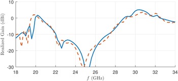
Fig. 11. Simulated (—) and measured (- -) frequency dependence of the realized gain in θ = 0°, ϕ = 0° direction.
Figure 12 depicts two measured and simulated farfield cuts of the realized gain in the xz-plane (H-plane) and the yz-plane (E-plane). In the measurement the antenna is rotated on a 1D-rotational positioner. Due to the previously observed frequency shift, slightly different frequencies are used in simulation (20.3 GHz) and measurement (19.95 GHz), which allows for a better comparison. Again, the 50 Ω-resistors are not included in the simulation. The results show a relatively good agreement between measurement and simulation. The measured realized gain is lower than predicted, which can be partially caused by losses in the connector that are not modeled in the simulation. Bigger deviations are observable towards higher elevation angles |θ| > 50°. These can be attributed to the absorbers mounted next to the antenna (c.f. Fig. 10). The differences in the radiation pattern, when compared with Fig. 6, are mainly due to the increased size of the finite ground plane and the neighboring array elements. The measurement results for the second polarization port are not displayed since they are very similar.

Fig. 12. Simulated (—) and measured (- -) realized gain at 20 GHz (blue —) and 30 GHz (red ![]() ) with the signal source at port 1 in the xz-/H-plane (left) and yz-/E-plane (right).
) with the signal source at port 1 in the xz-/H-plane (left) and yz-/E-plane (right).
B) Feed network
To construct an array with multiple excited elements a feed network is required. One way to achieve this is to add more layers to the design, which would lead to a difficult manufacturing process. Thus, a network is developed that can be integrated on layer 5 together with the feed. It is based on cascaded wideband microstrip power combiners. One of these is depicted in Fig. 13(a). It consists of a T-junction with a stepped matching network. The input reflection is below −20 dB from 15 to 35 GHz at port 1 and both transmission coefficients are in the expected range (c.f. Fig. 13(b)). Due to the symmetric design, there is no difference between port 2 and 3.

Fig. 13. (a) Illustration of the designed wideband power combiner. (b) Simulated S-parameters of the lossless network.
The above combiner is too large for the last stage of the cascaded network close to the antenna element. A modified version fitting in the 5 mm array grid and preventing overlaps with the tuning fork shaped feeding structure beneath is depicted in Fig. 14(a).

Fig. 14. (a) Illustration of the designed power combiner with chamfered corner and signal vias to feed the upper polarization ports of two neighboring antennas. (b) Simulated S-parameters of the lossless network.
The corner is chamfered to improve the matching. The signal vias to the upper polarization port are included in the network. The close proximity of the microstrip lines from port 1 and 3 cause parasitic coupling, that yields an unsymmetrical response as observed in Fig. 14(b). Input matching at port 1 is deteriorated in comparison with the design in Fig. 13. More importantly, there is a phase and amplitude imbalance between ports 2 and 3 of roughly 1 dB and maximal 7°, respectively. This can be tolerated for the array design, since this divider is used directly at the antennas and is not cascaded. However, this increases sidelobes in array applications.
C) 4 × 4 Antenna array
To demonstrate the functionality of the proposed arrangement two 4 × 4 arrays with fixed beams pointing at θ = 0° and θ = −30°, respectively, are realized. Only one polarization is considered as dual- polarization networks would require additional PCB layers, thus increasing the circuit complexity without adding much insight. To minimize edge effects 12 elements are placed around the central 4 × 4 array. Figure 15 shows the backside of the two arrays with dedicated feed networks.

Fig. 15. Feed networks on the backside of the 4 × 4 antenna arrays with the main beam in (a) θ = 0° direction and (b) θ = −30° direction.
The networks consist of three wideband combiners and an angled version directly at the antenna feed points. The array in Fig. 15(a) has equal distances from the feed point at the coaxial connector to all elements, so that its main beam is pointed at θ = 0°. The close proximity of the array elements and the combiner stresses the necessity for the angled version of Fig. 14(a). The second array in Fig. 15(b) differs in that two of the three wideband combiners are asymmetric. The resulting time delay τ tilts the main beam to θ = −30° at both operating frequencies.
The arrays performance is measured using the previously described method. In Fig. 10, 4 × 4 array with edge elements is shown on the positioner. The obtained farfield cuts are plotted in Fig. 16. It can be observed, that the array beams are tilted as designed and feature approximately 10 dBi gain in both bands. As expected, the sidelobe level is increased when the array is scanned. For comparison a full-wave simulations is performed using an exact geometric model of the arrays without the coaxial connector. The feed networks as well as losses are included. Since the simulation did not indicate a significant influence of the 50 Ω terminations they are included in neither the simulation model nor the measured array.

Fig. 16. Simulated (—) and measured (--) realized gain at 20 GHz (blue —) and 30 GHz (red ![]() ) in the yz-cutting plane with the beam pointed to θ = 0° and θ = −30°.
) in the yz-cutting plane with the beam pointed to θ = 0° and θ = −30°.
Generally, the simulated and measured performance are in good agreement, thus validating the taken approach. Beam direction and width coincide well. Similarly to the single elements, some discrepancy is observed at higher elevation angles. This is due to the absorbers mounted next to the antenna. In contrast to an ideal array, a relatively high sidelobe can be observed, especially in simulation. This is attributed to the imbalance of the feed network and the residual coupling within the feed structure and the array. Manufacturing errors might also play a role.
V. CONCLUSION
A multilayer planar dual-band patch antenna with two polarization ports is introduced for Ka-band satellite applications. The design is explained and the antenna is evaluated in detail. The resulting patch size is compatible with the grating lobe requirements of scannable arrays. The antenna is fabricated and validated through measurements. The results are in good agreement with simulation. The measured input reflection is low with only a minor frequency shift. The circular polarization characteristics of the antenna are very good in both bands over a wide angular range.
The patch design is tested in different array arrangements to comprehensively assess its performance. Simulated and measured S-parameter and farfield results validate the taken approach. The design's suitability to build larger arrays is demonstrated through analysis of two 4 × 4 antenna arrays pointing at different angles. In conclusion, the proposed antenna design is well suited for integrating transmit and receive terminals in larger Ka-band communication arrays.
ACKNOWLEDGEMENTS
The authors wish to acknowledge the funding of this work by the German Aerospace Center (DLR) on behalf of the German Federal Ministry of Economics and Technology (BMWi) under research contract 50YB1302.
 Benjamin Rohrdantz is currently working towards a doctoral degree at the Institute of High Frequency Technology, Hamburg University of Technology, Germany. He received the Dipl.-Ing. degree in Electrical Engineering in 2009. Since then he has worked on different research projects that explore phased array and active antenna systems for applications such as satellite communications and radar. His research interests include electronically scanned arrays, passive circuits, component packaging, and new fabrication technologies.
 Thomas Jaschke was born in Hamburg, Germany in 1988. He received the B.Sc. and the M.Sc. degree from the Hamburg University of Technology, Hamburg, Germany in 2010 and 2012, respectively. Since 2012, he is a Ph.D. student at the Institute of High Frequency Technology, Hamburg University of Technology, Germany. His research interests include phased arrays, passive components, electromagnetic theory, and antenna measurement.
 Frauke Gellersen was born in 1988. She studied electrical engineering and received the M.Sc. in 2013 from the Hamburg University of Technology (Technische Universität Hamburg), Germany, where she is since then working towards her doctoral degree. Her research focuses on ferrite materials and nonreciprocal components for self-biased microwave devices.
 Anton Sieganschin was born in Barnaul, Russia 1992. He received the B.Sc. degree in Electrical Engineering from Hamburg University of Technology in 2015. He is currently working towards a Master's degree in Microwave Engineering, Optics, and Electromagnetic Compatibility. His current research interests include planar microwave circuits and antenna feeding networks.
 Arne F. Jacob received the Dipl.-Ing. degree in Electrical Engineering in 1979 and the Dr.-Ing. degree in 1986 from the Technische Universität Braunschweig, Germany. From 1986 to 1988 he was a Fellow at CERN, the European Organization for Nuclear Research, Geneva, Switzerland. In 1988 he joined Lawrence Berkeley Laboratory, University of California at Berkeley for almost 3 years as a Staff Scientist at the Accelerator and Fusion Research Division. In 1990, he became a professor at the Institut für Hochfrequenztechnik, Technische Universität Braunschweig. Since 2004 he has been a professor at the Technische Universität Hamburg, Germany, where he heads the Institut für Hochfrequenztechnik. His current research interests include the design, packaging, and application of integrated (sub-)systems up to millimeter frequencies, and the characterization of complex materials. Arne Jacob is a Fellow of the IEEE, a member of the VDE-ITG, the EuMA, and the URSI Commission B.


