I. INTRODUCTION
Solid-state power amplifiers (SSPA) for spacecraft transmitters are multistage power combined structures that are prone to exhibit odd-mode parametric frequency division oscillations, among other undesired behavior [Reference Kassakian and Lau1–Reference Elad, Shaulsky and Mezhebovsky9]. The most common procedure for the elimination of such instabilities is to add series and shunt resistors. However, circuit stabilization usually relies on empirical knowledge and the selection of the value and the position of these resistors are not generally issued from an in-depth large-signal stability analysis. For instance, it is common practice to introduce inter-branch resistors between all the transistor drains and between all the transistor gates, to diminish the risk of odd-mode parametric oscillations in microwave FET-based amplifiers [Reference Wang, Suarez and Rutledge7, Reference Suarez10]. Nevertheless, these inter-branch resistors can entail a negative impact on the amplifier radio frequency (RF) performances when the technological dispersion breaks the perfect symmetry of the design or when the circuit topology forces the use of electrically long transmission lines (visible for both even and odd-modes) to connect these resistors with the main RF paths. Besides, the parallel Resistor-Capacitor (RC) networks are often included by default in series with the transistor gates or bases as an additional measure to guarantee the absence of spurious signals at the divided-by-two frequency (f in/2). Although such networks are usually conceived to reduce the gain at f in/2, the gain at the fundamental frequency f in is also affected. In addition to that, these RC networks also have a negative contribution to self-biasing effects. In general, all these procedures are not correlated to rigorous large-signal stability analyses and are too conservative. Therefore, they can negatively impact amplifier performances at the operating frequency band (lowering gain, output power, efficiency, etc.).
In the present work, authors report on an enhanced approach for the design of RF and microwave SSPAs in order to improve it through a more efficient use of stability analysis techniques from the initial steps of the design. In particular, pole-zero stability analysis techniques [Reference Jugo, Portilla, Anakabe, Suárez and Collantes11] are used here in order to reduce the amount of stabilization networks, while maintaining a sufficient stability margin. This margin is verified through Monte Carlo large-signal stability analyses that account for process variability [Reference Collantes, Otegi, Anakabe, Ayllon, Mallet and Soubercaze-Pun12].
II. SYSTEMATIC OPTIMIZATION APPROACH
The presented procedure consists of integrating the pole-zero large-signal stability analysis from the early stages of the design, when no stabilization networks are yet applied. In this situation, power-combining structures with two or more transistors in parallel will likely present critical poles around half the frequency of the input drive, f in/2, for certain levels of input frequency, RF power and/or bias values [Reference Suarez10]. These critical poles are often associated with an odd-mode resonance around f in/2 that takes place when the non-linear input capacitances of the combined transistors are pumped by the input drive [Reference Suarez10]. Therefore, if the potential odd-mode instability is detected when no stabilization networks are acting on the amplifier, it can be controlled and suppressed by applying consequently the minimum and sufficient stabilization networks that less deteriorate RF performances. For that, a combined RF and large-signal stability optimization is performed at the same time, in order to achieve an optimum design in terms of RF performances and stability of the periodic steady-state solution.
The large-signal stability analysis is based on obtaining a single-input, single-output (SISO) closed-loop transfer function of the circuit linearized about a given periodic large-signal steady state. For the linearization, the usual practice is to insert a small-signal current source at an arbitrary node of the circuit [Reference Jugo, Portilla, Anakabe, Suárez and Collantes11]. A mixer-like analysis based on the conversion matrix is performed, where the periodic large-signal steady state is calculated first. Around this periodic steady state, the frequency of the small-signal perturbation source is swept in order to obtain the frequency response of the circuit [Reference Jugo, Portilla, Anakabe, Suárez and Collantes11]. The total impedance seen by the perturbation source represents the closed-loop response H(jω) of the linearized system. Once the frequency response is obtained, automatic pole-zero identification techniques [Reference Anakabe, Ayllon, Collantes, Mallet, Soubercaze-Pun and Narendra13] are applied to calculate its associated transfer function H(s), as a ratio of two polynomials. Except for exact pole-zero cancellations, poles of H(s) determine the local stability of the particular steady state under analysis. Exact pole-zero cancellations can actually take place at certain combination nodes in a multistage power combined amplifier because, due to the symmetry, they are virtual ground for odd-mode oscillations. Indeed, performing the identification at different combination nodes, as suggested in [Reference Anakabe, Collantes, Portilla, Mons and Mallet8], the predominant oscillation mode can be detected.
Monte Carlo stability analyses are also used during the process to assess large-signal stability margins with respect to process variations. The following flow is therefore adopted during the optimization process:
1. Apply pole-zero identification to detect the potential oscillations when no stabilization networks are included. Identify the operating conditions that lead to the instability and the predominant odd-mode oscillation performing the identification at different combination nodes [Reference Anakabe, Collantes, Portilla, Mons and Mallet8]. If oscillation mode is even go to step 4. If oscillation mode is odd (more likely case in power combining amplifiers) then step 2 follows.
2. Attempt to stabilize the circuit by consistently connecting inter-branch resistors at the latter stages of the amplifier according to the predominant mode of oscillation. This allows the use of shorter transmission lines with less impact on matching networks. If no instability is detected in this case for any of the operating conditions of interest, step 5 must follow. If otherwise these inter-branch resistors are not enough to eliminate the instability or to achieve the required stability margin, step 3 is the next step in the flow.
3. At this step, inter-branch resistors at other stages should be added according to the predominant mode of oscillation identified in step 1. Parametric large-signal stability analyses will indicate the best values that are compliant with stability margin requirements. The longer stubs connected to these inter-branch resistors may shift the frequency response of the matching networks. If it is the case, they have to be re-tuned and stability must be re-ascertained afterwards. Again, if no stability problem is detected, step number 5 follows. If otherwise more stabilization networks are needed, step number 4 is the next on the flow.
4. Here, parallel RC networks in series with the transistor gates (or bases) have to be added symmetrically until the required large-signal stability margin is achieved. This type of stabilization networks is the last solution to be used due to its negative influence on RF performances at the fundamental frequency. At this stage, stability will be ascertained for certain values of the RC network and step number 5 will follow. Parallel RC networks will be requisite if the oscillation is even mode.
5. Monte Carlo stability analyses are performed at this stage of the process in order to ensure stability margins against technological dispersion that is inherent to variations of the monolithic microwave integrated circuit (MMIC) foundry process. If any of the solutions of the Monte Carlo analysis shows either unstable poles or critical poles not compliant with stability margin requirements, step 2 (step 4, in the case of even mode) needs to be revisited either to modify resistor values or to add more stabilization resistors. Otherwise, the process finishes here.
At the end of the process, the design will present an optimum solution in terms of stability and RF performances for the particular bias and RF input conditions.
III. APPLICATION EXAMPLE
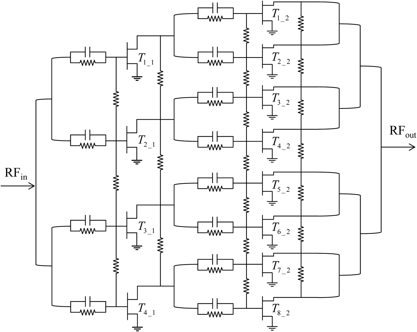
In order to illustrate the capabilities of the presented approach, a Ku-band MMIC high-power amplifier (HPA), conceived for an active antenna space application, has been analyzed. The HPA has been designed and measured at Thales Alenia Space – France with the support of the French Spatial Agency (CNES). A space-qualified GaAs 0.25 µm gate-length pHEMT manufacturing process has been used. Measurements of the fabricated MMIC reported 4 W output power, 20 dB gain and 40% power-added efficiency (PAE) in 2 GHz bandwidth [Reference Ayllon, Collantes, Anakabe, Lizarraga, Soubercaze-Pun and Forestier14]. The HPA has a two-stage topology with four and eight parallel transistors in the first and second stages, respectively (Fig. 1). It presents inter-branch resistors of 15 Ω between all the transistor gates and drains as well as parallel stabilization RC networks connected in series to all the transistor gates.

Fig. 1. Simplified schematic of the initial MMIC HPA.
Monte Carlo large-signal stability analyses were carried out in the initial circuit of Fig. 1. In particular, 100 trials were performed during each Monte Carlo stability analysis. Technological dispersion inherent to variations of the MMIC foundry process was taken into account. The small-signal current source is connected between the gates of transistors 4 and 5 of the second stage. The circuit shows a stable operation for every value of RF input power, input frequency and bias condition of interest. As an example, Fig. 2 shows Monte Carlo results obtained when the initial circuit of Fig. 1 is operated at f in= 12.7 GHz and 4 dB compression.
Fig. 2. Monte Carlo large-signal stability analysis of the initial HPA for f in = 12.7 GHz and 4 dB compression. × are the poles.
The HPA remains stable with all the critical poles around f in/2 located on the left-half plane (LHP) of the complex plane. Note that, among the 100 trials, only few trials present poles at f in/2. The position of these poles on the LHP will be used as the qualitative goal to be achieved in terms of stability margins during the large-signal optimization approach.
As indicated in the first step of the optimization algorithm, all the stabilization networks are eliminated and large-signal stability is analyzed. As expected, the HPA reveals a parametric odd-mode oscillation at f in/2 under several conditions of RF input power, input frequency and bias level. For instance, Fig. 3 shows the frequency response and the associated pole-zero identification results when the amplifier is operating at 12.7 GHz, 4 dB compression level. The analysis yields a pair of unstable complex conjugate poles at f in/2 on the right-half plane (RHP) of the pole-zero plot, revealing an odd-mode parametric instability at f in/2. An analysis of the odd-mode instability is also performed where the predominant oscillation mode detected is [++++−−−−], i.e.: transistors T 1_2, T 2_2, T 3_2, and T 4_2 oscillate in phase, but 180° out-of-phase with transistors T 5_2, T 6_2, T 7_2, and T 8_2.
Fig. 3. (a) Frequency response (crosses) and associated identification results (solid line) of the MMIC HPA stability analysis without stabilization networks around f in/2, with f in = 12.7 GHz and 4 dB compression level. (b) Pole-zero identification results revealing the instability at f in/2.
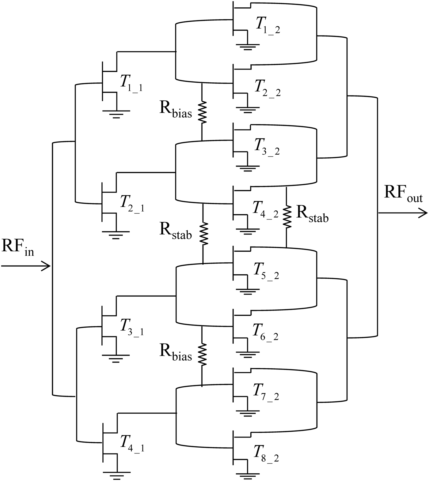
Once the spurious oscillation has been detected, step 2 of the combined RF and large-signal stability optimization procedure follows. The oscillation mode being [++++----], the optimum location for the stabilization resistors connected with shorter lines is between the gates and drains of transistors T 4_2 and T 5_2 (see Fig. 4). Since simulations showed that stability can be achieved with these two resistances, Monte Carlo analysis (step 5) follows. Two other inter-branch resistances (R bias, between gates of transistors T 2_2, T 3_2 and gates of transistors T 6_2, T 7_2) have been considered in the analysis (Fig. 4). These two resistances are required by the circuit topology for biasing the gates of transistors T 3_2, T 4_2, T 5_2, and T 6_2. Therefore, they are maintained in the analysis although they have a minor effect on the stabilization of the predominant mode. At the same time, input and inter-stage matching networks have been readjusted to adapt the circuit to the new stabilization configuration. As a result of the Monte Carlo analysis (Fig. 5), a value of R stab = 15 Ω has been enough to attain stability margins comparable to the initial circuit. The two R bias have also been set to 15 Ω. Note that, for this particular example all the series RC networks and all the inter-branch resistances of the first stage (the ones with longer lines) have been eliminated.
Fig. 4. Final topology of the optimized MMIC HPA. Four inter-branch resistors have been used to stabilize the amplifier.
Fig. 5. Monte Carlo large-signal stability analysis of the optimized HPA for f in = 12.7 GHz and 4 dB compression. × are the poles.
As an example, Figs 6 and 7 show respectively a comparison of the simulated RF output power and PAE when f in = 12.7 GHz.
Fig. 6. Output power versus input power of the initial (solid line) and optimized (dashed line) circuits at f in = 12.7 GHz.
Fig. 7. PAE versus input power of the initial (solid line) and optimized (dashed line) circuits at f in = 12.7 GHz.
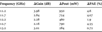
For this particular input conditions, the optimized version of the MMIC design reports an improvement of 2.16 dB (>10%) in Gain, 790 mW (>22%) in output power and 4.55 points (>10%) in PAE at 2 dB compression point, as compared to the initial version. Furthermore, the optimized circuit remains stable and shows comparable large-signal stability margin results. The same trend is encountered over the entire operation bandwidth, yielding enhanced RF performances as compared to the initial version of the MMIC HPA. Table 1 summarizes the enhancement in RF performances for the optimized version of the MMIC HPA, as compared to the initial version. Results are compared when the amplifier is operating at 2 dB compression.
Table 1. RF performance improvements after the optimization process of the MMIC HPA.
IV. CONCLUSION
An enhanced approach in the design of RF and microwave SSPAs has been presented. Rigorous large-signal pole-zero stability analysis techniques have been used all over the optimization process to help reducing the amount of stabilization networks that may deteriorate the RF performances at the fundamental frequency of operation, while preserving similar stability margins. The technique has been applied for the optimization of an MMIC HPA for space-borne applications. As a result, an improved and optimized MMIC design has been obtained with lesser amount of stabilization networks, achieving comparable stability margins and better RF performances over the entire bandwidth of operation.
ACKNOWLEDGEMENT
Authors from UPV/EHU wish to acknowledge the Spanish and Basque Administrations for partially supporting this work through projects TEC2009-09874 and IT456-10, respectively.
 Natanael Ayllon received the Ph.D. degree in Microwave Engineering from the University of the Basque Country (UPV/EHU), Bilbao, Spain, in 2011. From 2006 to 2011, he was a Research Engineer at the Electricity and Electronics Department of UPV/EHU, where he was involved in linear and non-linear stability analysis of microwave circuits, MIC/MMIC design, manufacture, and measurement techniques of such circuits. Since 2011, he is with the European Space Agency ESA-ESTEC, where he supports the development of future GNSS payloads and HPA development activities for space-borne applications.
Juan-Mari Collantes received the Ph.D. degree in electronics from the University of Limoges, France, in 1996. Since February 1996, he has been an Associate Professor with the Electricity and Electronics Department, University of the Basque Country (UPV/EHU), Bilbao, Spain. In 1996 and 1998, he was an Invited Researcher with Agilent Technologies (formerly the Hewlett-Packard Company), Santa Rosa, CA. In 2003, he was with the French Space Agency (CNES), Toulouse, France, where he was involved with power amplifier analysis, simulation, and modeling. His areas of interest include non-linear analysis and design of microwave circuits, microwave measurement techniques, and noise characterization.
 Aitziber Anakabe received the Ph.D. degree in electronics from the University of the Basque Country (UPV/EHU), Bilbao, Spain, in 2004. In 1999, she joined the Electricity and Electronics Department, UPV/EHU, where she was involved with the stability analysis of non-linear microwave circuits. In 2004, she joined the French Space Agency (CNES), Toulouse, France, as a Post-Doctoral Researcher. In 2005, she rejoined the Electricity and Electronics Department, UPV/EHU, where, since 2005, she has been an Associate Professor. Her research deals with non-linear analysis and modeling of microwave circuits and measurement techniques.
Geoffroy Soubercaze-Pun received his Ph.D. degree in Electronics from the University of Toulouse (France) in 2007. He has first worked for Thales Alenia Space France on frequency synthesis. In 2008, he joined the French Space Agency (CNES), Toulouse, France. His main research interests are power amplifiers and non-linear analysis of microwave circuits.
 Stephane Forestier received the Electrical Engineering degree from the Ecole Polytechnique de l'Université de Nantes (EPUN) in 2000. He received the Ph.D. degree in microwave communication engineering from the University of Limoges in 2003. In 2000, he joined IRCOM. He was involved with high-power amplifier design methods and linearizer systems. In 2004, he joined Thales Alenia Space, Toulouse, France, where at present he is an Advanced Study Engineer involved in topics related to high-power applications such as characterization, modelization, simulation, and design. Since 2010, he is in charge of telecom satellite payload architecture.
Dominique Langrez was born in France, in 1966. He received the Ph.D. degree in electronics from the University of Science and Technology of Lille, Lille, France, in 1996. In December 1996, he was an R&D Microwave Engineer with the MMIC Design Department of Alcatel Alenia Space, Toulouse, France, where he was involved in the designing of monolithic microwave integrated circuits for telecommunication applications encountered in radio links, Earth-based stations, and payload satellites. He is currently the Head of the Microwave Building Block Design Group at Thales Alenia Space.