I. INTRODUCTION
In the last few years, antenna engineers have shown great interest in composite periodic structures such as electromagnetic bandgap (EBG) and metamaterials due to their unique physical properties and novel applications [Reference Yang and Rahmat-Samii1–Reference Veselago and Lebedev3]. EBG inhibits propagation of electromagnetic (EM) waves in certain range of frequency called bandgap, which depend on its geometrical and material parameters [Reference Sievenpiper, Zhang, Broas, Alexopolous and Yablonovitch4]. Hwang and Peng [Reference Hwang and Peng5] used the mushroom-type EBG to reduce the mutual coupling between elements of an antenna array. Jackson et al. [Reference Jackson, Williams, Bhattacharyya, Smith, Buchheit and Long6] describe a microstrip patch antenna, which do not excite surface waves with the help of a two-dimensional (2D) EBG structure. Similarly, metamaterial approach has been extensively used as a promising method to obtain high-performance antennae [Reference Caloz and Itoh7]. Zhu et al. [Reference Zhu, Lin and Hu8] used a metamaterial consisting of copper grids with square lattices for directive emission. A metamaterial consisting of inverted S-shaped metallic ring array was used by Wu et al. [Reference Wu, Yeb and Lu9] to improve antenna gain. Wu et al. [Reference Wu, Wang, Pacheco, Chen, Grzegorczyk and Kong10] describe the use of various metamaterial structures as substrate of patch antenna to improve its gain. While these approaches show good improvements in antenna performance individually, the improvements would be much better when both EBG and metamaterial are used simultaneously with an antenna. However, simultaneous application of EBG and metamaterial suffer complications due to their different geometry and design. Hence, there is stringent requirement of a structure, which can exhibit the properties of both EBG and metamaterial to effectively utilize the advantages of both composites with a single design.
In this paper, we present a structure based on double cross strips printed on both sides of a dielectric, which shows the behavior of both EBG and metamaterial. The structure is investigated on CST Microwave studio [11] and its transmission coefficients and retrieved EM parameters exhibit its bandgap characteristics and left-handed (LH) behavior for propagation in two different planes. Furthermore, this structure is used as a substrate as well as superstrate of a microstrip patch antenna operating at 11 GHz to improve its performance by suppressing surface waves and focusing the radiated field.
II. INVESTIGATION OF METAMATERIAL BEHAVIOR
The unit cell of the structure is given in Fig. 1(a), which consists of double-crossed metallic stripes printed on both sides of a dielectric substrate. The parameters of the structure are optimized to obtain LH behavior about 11 GHz. Transmission line (TL) theory can be applied to understand the LH behavior of the proposed structure [Reference Zouhdi, Sihvola and Vinogradov12]. The printed stripes on both sides of substrate can be modeled as inductors which are connected by capacitors formed by substrate sandwiched between metal plates on both side. This theory suggests that the proposed metamaterial is a resonating-type structure having some resonant frequency depending on the values of inductance and capacitance.

Fig. 1. The structure to work as a metamaterial. (a) Unit cell having dimensions L = 13.6 mm, w = 0.7 mm, h = 3.5 mm, and dielectric constant of the substrate is 3.7. (b) Transmission coefficients.
It has been shown that a structure composed of a periodic mesh of metallic thin wires, when its characteristic dimensions (period, section of the wires) are small in comparison to the wavelength, behaves as a homogenous material with a low plasma frequency [Reference Pendry, Holden, Robbins and Stewart13–Reference Felbacq and Bouchitte14]. When the structure is simulated under plane wave incidence normal to its plane, the electric field varies continuously along the length of the conductors and behaves like a continuous plasma medium having the specific plasma frequency [Reference Sigalas, Chan, Ho and Soukoulis15]. This continuous plasma medium gives rise to negative permittivity below the plasma frequency. Time-varying magnetic field induces a current loop between the two layers of metallic stripes consisting of both conduction and displacement currents that give rise to magnetic moment. The induced magnetic moment opposes the applied magnetic field. This behavior is similar to diamagnetic materials, which result in negative permeability at the resonant frequency.
Effective medium theory and homogenization procedure are adopted to calculate the EM properties of the proposed structure such as effective wave impedance (Z eff) and effective refractive index (N eff), from the scattering parameters of the periodic structure, for a normal incidence of plane wave [Reference Szabó, Park, Hedge and Li16].
 $${Z_{eff}}=\pm \sqrt {\displaystyle{{{{\left({1+{S_{11}}} \right)}^2}- S_{21}^2 } \over {{{\left({1- {S_{11}}} \right)}^2}- S_{21}^2 }}}\comma \;$$
 $${e^{iN{k_0}d}}=\displaystyle{{{S_{21}}} \over {1 - {S_{21}}{R_{01}}}}\comma \;$$
where N(ω) = n eff(ω) − ik eff(ω) and R 01 = (Z eff − 1)/(Z eff + 1). The sign of (Z eff) is decided by effective medium conditions, i.e. Re(Z eff) ⩾ 0 and Im(N eff) ⩾ 0. Finally by inverting the relations  $N_{eff}=\sqrt{{\varepsilon _{eff}}{{\rm \mu} _{eff}}}$ and
  $Z_{eff}=\sqrt{{\mu _{eff}}/{\varepsilon _{eff}}}$ the effective permittivity and effective permeability are calculated.
The scattering parameters are shown in Fig. 1(b) and the effective medium parameters such as effective permittivity and effective permeability of the structure are given in Fig. 2. It is clear from these parameters that the real part of effective permittivity and effective permeability are negative, simultaneously over a band of frequency, which will result in a negative value of refraction index in that frequency band. The positive value of imaginary part of effective refractive index and real part of effective wave impedance in Figs 2(c) and 2(d) fulfills the condition for passive medium.
Fig. 2. Retrieved parameters of the structure. (a) Effective permittivity, (b) effective permeability, (c) effective refractive index, and (d) effective impedance of the medium.
III. INVESTIGATION OF EBG BEHAVIOR
The same design with tailored dimensions of Fig. 1 is simulated under plane wave incidence in plane of the material to investigate the bandgap characteristics of the structure as shown in Fig. 3(a). As the structure interacts with EM waves, currents are induced in the top and bottom metal plates. This field applied parallel to the top surface causes charges to build up on the ends of the parallel plates, which can be described as a capacitance. As the charges slosh back and forth, they flow around a long path through the plates. Associated with these currents is a magnetic field and, thus, an inductance.
Fig. 3. EBG structure. (a) same unit cell of Fig. 1 is used to realize the EBG behavior with dimensions L = 3 mm, w = 0.2 mm, h = 0.5 mm, and dielectric constant of the substrate is 3.7; (b) S-parameters showing a bandgap in 8–14 GHz band.
Now, the surface impedance is equal to the impedance of a parallel resonant circuit, consisting of the sheet capacitance and the sheet inductance
 $$Z=\displaystyle{{j\omega L} \over {1- {\omega ^2}LC}}.$$
The surface is inductive at lower frequencies, and capacitive at higher frequencies. The impedance is very high near the resonance frequency
 $${\omega _0}=\displaystyle{1 \over {\sqrt {LC} }}.$$
We associate the high impedance with a forbidden frequency bandgap. Hence, by selecting the values of inductance and capacitance we can model the bandgap at a desired frequency range.
The parameters of the structure are optimized to offer high impedance about 11 GHz frequencies. The simulated transmission coefficient of the structure, given in Fig. 3(b), shows a clear bandgap for 8–14 GHz band. In this band, the structure behaves as high-impedance medium for the wave traveling in the plane of the structure. The variation of bandgap for multiple values of dielectric constant (εr) and periodicity (L) is given in Figs 4(a) and 4(b). Clearly the high-impedance region shifts in inverse proportion of length and dielectric constant.
Fig. 4. Variation in bandgap characteristics for different value of: (a) dielectric constant and (b) periodicity (length of strips).
IV. ANTENNA DESIGN AND ITS SURFACE WAVE SUPPRESSION
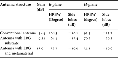
A microstrip patch antenna resonating at 11 GHz is designed as shown in Fig. 5(a). It consists of a rectangular patch placed on a substrate with ground plane at the bottom. When it is excited by a co-axial feed, it radiates EM energy in the vertical direction due to formation of fringing fields around the patch slots [Reference Balanis17]. The return loss of the antenna is found nearly −10 dB at 11 GHz as shown in Fig. 5(b) (red line), and the corresponding gain about 5.64 dB as seen from 3D far-field pattern in Fig. 6(c). The polar plot of the radiation pattern in the x–z plane (for Phi = 0°), shown in Fig. 8(a), indicates that this antenna radiates in a broad angle of 108.3°.
Fig. 5. (a) Microstrip patch antenna design with dimensions L = W = 30 mm, lp = 6 mm wp = 8.5 mm, h = 1.5 mm, and t = 0.5 mm; (b) return loss of the patch antenna (red line) and antenna on EBG substrate (blue line); (c) antenna design on EBG substrate perspective view; and (d) side view.
Fig. 6. (a) Near-field variation in conventional patch antenna showing surface wave, (b) near-field variation in EBG antenna showing suppression of surface wave, (c) 3D far-field pattern of conventional antenna, and (d) 3D far-field pattern of antenna on EBG substrate.
A significant amount of energy gets trapped into the substrate resulting in unwanted surface wave loss, which if suppressed can enhance the gain of the antenna [Reference Balanis17].
To suppress the surface wave, the EBG structure designed in the last section is used as a substrate of the patch antenna (Figs 5(c) and 5(d)). The EBG layer is sandwiched between two lower dielectric substrates and the metal strips below the patch is removed to reduce the direct excitation of the strips by the feed. Within its bandgap, around the resonant frequency of the antenna, it does not allow surface waves to propagate in the substrate; as a result, the whole field is radiated in vertical direction by patch and enhances the gain. Figs 6(a) and 6(b) give a clear picture of surface wave suppression by the EBG substrate. Owing to this the return loss is improved to −18.5 dB (Fig. 5(b) blue line) and the far-field pattern, in Fig. 6(d) depicting gain of 9.21 dB, shows a gain improvement of 3.57 dB as compare to conventional antenna due to suppression of surface waves.
V. ANTENNA WITH EBG SUBSTRATE AND METAMATERIAL COVER
To further improve the performance of the antenna, 12 × 12 periodic cells of the metamaterial designed in Section II is placed as a superstrate of the antenna as shown in Fig 7(a). Since the cover is a LH material having negative index of refraction, it shows congregation effect for radiation incident on it [Reference Yang and Zhao18], which is similar to the case when light wave passes through a convex lens. Here, the distance between the patch and the metamaterial ‘d’ has been optimized to a value of 32 mm to obtain better focusing effect. The 3D radiation pattern of the combined structure in Fig. 7(b) shows more than two times improvement in gain as compared to the conventional antenna value. This improvement in gain clearly depicts that the radiation characteristics of the antenna has been improved due to the metamaterial cover.
Fig. 7. (a) Microstrip patch antenna on EBG substrate with metamaterial cover, (b) its 3D radiation pattern, (c) radiation pattern from the patch antenna alone, and (d) with metamaterial cover.
Without the cover, emission from the patch antenna is distributed over broad angle due to its spherical wave front; hence its directional gain is very low, as observed in Fig. 7(c). Metamaterial converges the spherical wave front from the patch antenna into a flat pattern (Fig. 7(d).); as a result whole radiation adds up in normal direction. The part of radiated field incident around the central region of the metamaterial got collimated due to its lensing effect but the part incident at the edges of the metamaterial undergo scattering and suffers some losses. The enhancement in directivity of the antenna could be explained by considering the leaky wave propagating along the surface of the structure as in case of Fabory–Perot Antenna. The attenuation constant of such leaky wave, if known, provides means for designing the correct cover size to avoid diffraction effects [Reference Mateo-Segura, Goussetis and Feresidis19]. Figure 8 compares the polar plots of the far-field pattern, which clearly shows that the incorporation of metamaterial cover made the antenna highly directional by reducing its E-plane half power beam width (HPBW) to 32.7° from 108.3°. A complete picture of the effects of EBG substrate and metamaterial cover on the conventional patch antenna is clear from Fig. 9. It is also evident that the use of this EBG as a substrate significantly reduces the side-lobe level in far-field pattern. These all results have been summarized in Table 1.
Fig. 8. (a) Polar plot of radiation from conventional microstrip antenna, (b) polar plot of radiation of antenna on EBG substrate with metamaterial cover.
Fig. 9. Cartesian plot of radiation pattern showing gain of different designs.
Table 1. Comparison of gain and directionality of different antenna structures.
VI. CONCLUSION
Based on these results it is clear that the designed structure exhibits the bandgap properties of EBG as well as LH behavior of metamaterial. These properties make this structure unique and first of its kind which can suppress the surface waves when incorporated in substrate and shows the focusing effect on the radiation when used as superstrate of a microstrip patch antenna. The designed structure is planer and very easy to fabricate which can simply be incorporated with microstrip antenna. Hence, this structure could be a strong choice to eliminate the complications in design due to different geometry and design of EBG and metamaterial inclusions.
Anand Kumar is an Assistant Professor in the Department of Electronics and Communication Engineering at Jaypee Institute of Information Technology, Sector 128, Noida. He received his M.Tech. degree in Electronics and Communication Engineering from Indian Institute of Information Technology Design and Manufacturing (IIITDM), Jabalpur, India. His research interest includes electromagnetics, antenna and wave propagation, metamaterials, and electromagnetic bandgap structures.
Dinesh Kumar V. is an Associate Professor of Electronics and Communication engineering at Indian Institute of Information Technology Design and Manufacturing (IIITDM), Jabalpur, India. He received his Ph.D. degree in Electrical Communication Engineering from Indian Institute of Science, Bangalore in 2005. He was a visiting foreign researcher in Japan from 2006 to 2009. Prior to this, he was employed in Ministry of Communication and IT through Indian Engineering Services. His research interests include computational electromagnetics, microwave circuits, antenna and wave propagation, photonics, and optical communication.
Jitendra Mohan obtained his B. Tech. degree from S. R. T. M. University, Nanded in 1997. He got his M.Tech. degree from Aligarh Muslim University in 2005 and Ph.D. degree from Uttarakhand Technical University in 2011. He is currently working as an Assistant Professor in the Department of Electronics and Communication Engineering at Jaypee Institute of Information Technology, Noida (India). His main areas of interest are current-mode circuits and analog signal-processing applications. He has guided one Master's Dissertation and ten projects. He has more than 34 international journal and conference papers.
Hari Om Gupta received his B.E. degree in Electrical Engineering from the Government Engineering College, Jabalpur, India, and the M.E. degree in Systems Engineering and Operation Research and the Ph.D. degree from the University of Roorkee, Roorkee, India. He is currently a Professor and Director in the Jaypee Institute of Information Technology, Sector 128, Noida. Before joining there as Director, he was a Professor at Electrical Engineering Department, Indian Institute of Technology Roorkee till 2012. He visited McMaster University, Hamilton, ON, Canada, from 1981 to 1983 as a Postdoctoral Fellow. His research interests are in the area of database management, computer-aided design, reliability engineering, power network optimization, power transformers, and bioinformatics. He has over 300 publications to his name with 25 Ph.Ds supervised.