I. INTRODUCTION
Mode converters are commonly used for various applications, in which higher modes are advantageous. The key benefits of the TE01-mode in circular waveguides (CWGs) are its symmetric electrical field and the low wall-loss, which results from the specific field distribution. Furthermore, the field distribution is nearly insensitive against wall-disturbers. Thus, the TE01-mode is used in high-power applications like gyrotrons [Reference McDermott1] or plasma processing systems [Reference Kinder and Kushner2], due to its high-energy breakthrough threshold. In addition, low wall-losses can increase the dynamic range of level measurements in overmoded waveguides [Reference Pohl, Gerding, Will, Musch, Hausner and Schiek3]. Here, so-called bypass tubes are used for the determination of the level of liquids in storage or process tanks, when common antenna based radar systems cannot be applied [Reference Vogt4]. Due to disturbers such as stirrers, pipes, foam, waves, etc., common radar-based distance measurements and time-domain reflectometry-based measurements can be impaired dramatically [Reference Schulz, Will, Rolfes, Pohl, Baer and Musch5, Reference Gerding, Musch and Schiek6]. Hence, a bypass tube can be installed inside or outside the tank, as shown in Fig. 1, to measure the level of the liquid independent of these disturbers. Nevertheless, the following additional challenges can occur for level measurements in bypass tubes: (1) necessary openings for communicating vessel technique and (2) welded joints inside the tube can impair the measurement accuracy. (3) Deposited materials on the tubes wall can attenuate the measurement signal. (4) The radar target – the liquid itself or an additional float reflector – can cause transpolarizing effects of the incident wave and hence, the detected signal magnitude is reduced. (5) The tube itself represents an overmoded waveguide for the typically applied fundamental mode and additional modes can be excited, which impair the measurement accuracy as well. Hence, the TE01-mode is advantageous concerning these challenges. However, a mode converter is required for the excitation of this specific mode.

Fig. 1. Schematic depiction of five different challenges for bypass distance measurements of liquids in tanks for two application scenarios: (a) external placed bypass tube and (b) internal placed bypass tube.
Inline structures are a commonly used converter setup [Reference Matheson, Ronald, Speirs, Phelps and Cross7, Reference Krill and Zinger8] yielding a high suppression of disturbing modes using tapered waveguides. However, this results in long mechanical setups [Reference Davies, Davies and Saad9] and requires a precise manufacturing process. In contrast to this, side wall coupled setups can be realized in a more compact way [Reference Yu and Chang10], but with regard to several applications, side wall coupling is challenging and might not be applicable. Our approach is based on a stepped waveguide technique, which allows a compact setup, as we have presented in [Reference Schulz, Rolfes and Will11]. Combined with an inline coupling concept, a compact and broadband TE01-mode converter for the frequency range of 23 up to 28 GHz is achieved. Hence, the necessary frequency range for tank level probing radar regulated applications is completely covered by our mode converter.
The development of the converter is based on three-dimensional (3D) electromagnetic simulations to optimize the converter characteristics. Therefore, single elements are optimized at first and combined afterwards to the complete converter assembly. Based on these simulations a first prototype is realized and its functionality is verified by back-to-back measurements. The suitability for the described application is demonstrated by numerous measurements and the mode purity is proven by the characterization of the far-field of the mode converter.
II. MODE CONVERTER DESIGN
The presented converter design allows for an exceedingly broadband conversion of the CWG's fundamental TE11-mode into the TE01-mode, realized within a standard manufacturing process. With regard to industrial applications, the fundamental waveguide is of circular shape. Since a lot of industrial measurement systems make use of CWGs, the described converter can be applied easily to various measurement systems like the presented level measurements in bypass tubes. In addition, the setup includes a fundamental rectangular waveguide (RWG) and thus, comparisons with setups based on RWGs are possible. Since the TE01-mode is not the fundamental mode of CWGs, other higher modes have to be taken into account within the design process. Here, the TE11-, TM01-, TE21-, and TM11-mode can be excited as well, possessing cut-off frequencies below the desired TE01-mode. An effective suppression of these undesired modes is essential for the whole conversion concept. One possibility is the usage of symmetries within the setup to avoid the excitation of these undesired modes. Our approach makes use of two RWGs with a phase difference of 180° to suppress the TE11-mode. The TE21-mode can be suppressed using four RWGs positioned at 90° to each other, two pairs having a 180° phase difference. Nevertheless, transition elements are necessary to reduce reflections for good matching characteristics.
Regarding these specifications, the complete mode converter consists of the following parts, in order of appearance:
-
• One transition element from circular waveguide to rectangular waveguide (i).
-
• One rectangular signal divider (ii).
-
• Two 90° twists (iii).
-
• Two rectangular signal dividers (iv).
-
• Four 45° twists (v).
-
• One transition element transforming the four rectangular waveguides into the final circular waveguide (vi).
A schematic of the resulting converter design is depicted in Fig. 2. Here, the arrows inside the waveguides show the direction of the corresponding electrical field.

Fig. 2. Schematic depiction of the utilized mode converter design, showing the different waveguide positions. The inner arrows show the direction of the corresponding electrical field.
III. STEPPED WAVEGUIDE TECHNIQUE
Due to the various limitations of standard continuous waveguide technique, the so-called stepped waveguide technique is applied for the presented mode converter. Based on quarter wavelength parts – as initial value –, a significant shortened assembly can be realized compared with continuous waveguides without appreciable changes. As an example, Fig. 3 shows three different realization options for a 90° twist: (a) standard continuous waveguide, (b) split-block milled waveguide, and (c) single milled steps, which are combined to the final waveguide. Split-block technique is used for various rf- and terahertz-structures, as shown in [Reference Daniel12, Reference Bruneau, Janzen and Ward13]. However, many milling structures can get very complex and consequently uneconomic for industrial applications. The single milled steps are easy to fabricate, numerous waveguides can be produced within one plane with very small distances, different waveguide elements can be realized without limitations, and the resulting parts can be combined and stacked together afterwards to the final setup.

Fig. 3. Schematic depiction of different realization possibilities of a 90° waveguide twist: (a) continuous waveguide, (b) stepped waveguide in the split-block technique, and (c) single element stepped waveguide, which is applied for the presented mode converter.
Using equations (1) and (2), the cut-off frequencies of the different modes – TE mn and TM mn – for the RWG and CWG can be calculated, which dictate the resulting waveguide dimensions [Reference Pozar14]. For the RWG, with dimensions a and b, the cut-off frequency can be calculated as follows:
 $${f_{{\rm c}\comma mn}} = \,{c} \sqrt {{{\left({\displaystyle{m \over {2a}}} \right)}^2} + {{\left({\displaystyle{n \over {2b}}} \right)}^2}} .$$
For a CWG, with radius r, the cut-off frequency for TM mn - and TE mn -modes can be calculated by
 $$f_{{\rm c}\comma mn}^{\rm TM} = \displaystyle{{{c}{j_{mn}}} \over {2\pi r}}\quad \hbox{and}\quad f_{{\rm c}\comma mn}^{\rm TE} = \displaystyle{{{c}{{j^{\prime}}_{mn}}} \over {2\pi r}}\comma \;$$
respectively. Here j mn and j′ mn represent the roots of the Bessel function and its derivative, with j′11 = 1.841 for the TE11- and j′01 = 3.832 for the TE01-mode.
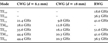
For the considered frequency range, a first CWG with a diameter of 8.2 mm and a second CWG with a diameter of 18 mm is applied for the excitation of the TE11-mode and the TE01-mode, respectively. For the different dividers and twist elements, a basic RWG with dimensions of 8 mm × 4 mm is used. The corresponding cut-off frequencies for the most important modes – calculated with (1) and (2) to be suitable for 23 up to 28 GHz – are presented in Table 1.
Table 1. Overview of the cut-off frequencies for the different waveguide dimensions applied for the mode converter.

IV. 3D ELECTROMAGNETIC SIMULATIONS
Based on the calculated waveguide dimensions and the presented mode converter design, different 3D models are investigated within CST Microwave Studio. Starting with the optimization of the necessary single elements, the final converter consists of a combination of these elements.
Realistic production process parameters are taken into account using bend edges of a 1 mm fillet and a minimal cutting width of 1 mm, while chamfer can be neglected for the chosen setup. Using the described limitations for the optimization process, an inverted setup has been chosen to speed up the simulation time dramatically. Here, the vacuum inside the waveguides is modeled within a perfect electric conductor (PEC). The boundaries are chosen to be electric (E tan = 0). Yet, an additional symmetry plane (magnetic: H tan = 0 or electric: E tan = 0) cannot be included for all single element models. Hence, just a few of the models are accelerated by additional symmetry planes. The transient solver and the perfect boundary approximation have proven to be suitable for the simulation of the single elements and the final complete converter. The hexahedral mesh definition is given by the “lines per wavelength” and the “lower mesh limit” set to 18 and 15, respectively. Furthermore, a “mesh line ratio limit” of 10 and a “simulation accuracy” of –50 dB have been chosen for the simulation. Depending on the highest considered frequency and the size of the simulation domain, this yields a mesh of approximately 4.2 million mesh cells for the complete converter, while the single parts can be simulated with a total amount of approximately 100 000 mesh cells. On a Dual Intel Xeon Octa-Core@3.1 GHz, this provides fast and sufficient simulation results for each setup within minutes.
A) Single element simulation
The six converter elements, described in Section II, are realized in seven different simulation models, as shown in Fig. 4. Due to the high importance of the final element – transformation of the four RWGs into the final CWG to excite the TE01-mode – this element is optimized in two steps: At first, the transition of the 45° twisted RWG into a quarter of the final CWG is optimized, followed by a combination of four of these elements ending in the final CWG. Here, the combined element is rotated by 180° for the single simulation. For all simulations, the waveguides in the front plane are used as excitation ports for the corresponding modes – TE11 for the first CWG, TE10 for the basic RWG, and TE01 for the second CWG – while the waveguides in the back plane are used as receiving ports. The simulated and optimized results are shown in Table 2 with the final amount of steps, the total length, and the corresponding reflection and transmission coefficients |S 11 |, |S 21 |, |S 31 |, |S 41 |, and |S 51 |. Here, the results represent a compromise between the amount of steps, their heights, and their specific properties. Nevertheless, a good return and insertion loss can be seen for all elements. Furthermore, the good dividing abilities are also obvious.

Fig. 4. Single elements of the mode converter within CST Microwave Studio for a fast and effective optimization: (i) transition element from CWG to RWG, (ii) and (iv) RWG signal divider, (iii) 90° twist, (v) 45° twist, (vi-a) transition element from RWG into a quarter of the final CWG, and (vi-b) transition element – rotated by 180° for the single element simulation – transforming the four RWGs into the final CWG.
Table 2. Overview of the optimization results of the single elements shown in Fig. 4.

B) Complete setup
The complete mode converter is realized as a combination of all single optimized elements. Hence, some of the first and last waveguides of the single elements can be combined to reduce the total amount of steps. A final optimization was performed on the resulting setup. Optimized in 34 single layers, possessing only five different heights – 2.26, 2.56, 2.7, 3.07, and 3.6 mm –, the mode converter has a total height of only 8.45 cm. The feeding is realized by a CWG port with a vertically polarized TE11-mode for a frequency range from 23 to 28 GHz, while both ports are defined to receive up to eight modes.
The resulting setup of the different converter parts and the corresponding magnitude of the electrical field in CST Microwave Studio are shown in Fig. 5 for a stepwise conversion from TE11- to TE01-mode.

Fig. 5. Mode converter within CST Microwave Studio: (a) 3D model of the complete setup designed with vacuum in PEC, (b) excitation with TE11-mode, (c)–(h) stepwise field distribution, and (i) received TE01-mode.
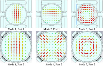
Figure 6 shows a selection of important modes at ports 1 and 2, which have to be considered for the investigation and optimization of the mode converter. Figure 7 shows the simulation results for the return loss, the insertion loss, the resulting time signals, and the transient reflection behavior of the optimized converter assembly. Here, the indices of the scattering parameters describe the ports as follows: S port(mode)port(mode) .

Fig. 6. Selection of important port modes in CST Microwave Studio, considered for the investigation and optimization of the mode converter.

Fig. 7. Simulation results of the optimized converter: (a) reflection coefficients |S 1(1)1(1)| and |S 1(3)1(1)| and transmission coefficient |S 2(7)1(1)| and |S 2(4)1(1)|, (b) time signals for the excited signal i 1(1), the reflected signal o 1(1)1(1), and the transmitted signal o 2(7)1(1), and (c) corresponding transient reflection behavior.
A good return loss better than 17 dB and an insertion loss below 0.1 dB can be observed for a frequency range from 23 to 28 GHz. This corresponds to an achievable bandwidth of approximately 20 % of the center frequency. The transmission coefficients |S 2(7)1(1) | and |S 2(4)1(1) | demonstrate the excellent mode conversion of the fundamental TE11-mode into the TE01-mode and the excellent suppression of higher modes, respectively. In addition, conversions into other modes at port 1 are suppressed by more than 60 dB and at port 2 by approximately 40 dB. Hence, a mode efficiency of over 99 % and a mode purity of over 99.9 % can be achieved.
The excellent characteristics can also be seen in the time signals of the transition: the time signals for the excited signal i 1(1), the reflected signal o 1(1)1(1), and the transmitted signal o 2(7)1(1), confirm the good transient behavior of the converter. Here, attenuation and dispersion effects are negligible and the reflected signal declines very fast. In addition, the transient reflection behavior yields a simple characterization of occurring reflections: a first reflection of approximately –30 dB results from the feeding into the first CWG and a second reflection of –24 dB results from a transition inside the converter. Multiple reflections are declining very fast and are reaching a level of –80 dB after 3 ns. Hence, the functionality of the mode converter is validated in frequency and time domain. Furthermore, no significant change can be observed for a tolerance investigation of the converter dimensions. To minimize the necessary amount of simulations, a random variation within a range of ±0.5 mm for the most critical parts and an angle tolerance of ±4° was investigated. Hence, the final setup represents a robust solution for industrial purposes.
C) Far-field simulations
For an evaluation of the mode purity of the converter and for a comparison with measurements in Section V, the far-field characteristics are evaluated within the simulations. Therefore, the setup is transformed into a PEC-based setup, the converter is excited by the fundamental TE11-mode at the first CWG, and the corresponding normalized far-field is evaluated for the two planes a − a′ and b − b′, as shown in Fig. 8(a). For evaluation, a radiated TE11-mode of an equal-sized CWG is shown in Fig. 8(b) for the E- and H-plane.

Fig. 8. (a) Simulation model of the mode converter made of PEC with two planes a − a′ and b − b′ and (b) simulated far-field characteristics for the fundamental TE11-mode in E- and H-plane and the desired TE01-mode in plane a and b.
The differences between the TE11- and TE01-mode are obvious. The TE01-mode shows its typical field distribution: minimum at 0°, symmetrical maxima at approximately ±35°, and continuous decrease to the edges.
V. REALIZATION AND MEASUREMENTS
Based on the performed simulations, two prototypes were manufactured. Here, the measurement assembly is arranged in a back-to-back configuration, using additional coaxial-to-CWG adapters for the direct connection of a vector network analyzer (VNA). The final mode converter is made of annealed brass and has a total length of 12.8 cm, including additional waveguide lengths for the adapters. Made of 34 layers, each layer is milled with a fillet radius of 1 mm as considered in the simulations. Two photographs of the realized converters are shown in Fig. 9. Here, aligning pins are used for a good positioning of the layers to each other. The whole setup is fixed by four screws in the edges to guarantee a close contact between all layers.

Fig. 9. Photographs of the produced mode converters in stepped waveguide technique.
A) Reflection and transmission behavior
For the measurements, a calibrated Rohde & Schwarz ZVK VNA with two additional coaxial-to-CWG adapters was used. Here, a CWG T(hrough) R(eflect) L(ine) calibration was applied. The resulting calibration reference plane is behind the transitions in the CWG. Hence, the resulting measurement setup consists of: VNA – coaxial-to-CWG – mode converter – mode converter – CWG-to-coaxial – VNA. The measurement results are shown in Fig. 10. The measurements of the reflection and transmission coefficients (index m) are compared with a simulation of an equal back-to-back configuration (index s), considering correct length and material parameters. A very good compliance between simulation and measurement can be observed for the whole frequency range. The return loss of the back-to-back transition is better than 12 dB, while the measured insertion loss is below 2 dB. This is affected by an additional mode conversion, additional material losses, and non-perfect alignments and connections of the layers. Both measurements demonstrate the suitability of the converter and allow for a further investigation.

Fig. 10. Comparison of the simulated (solid line) and measured (dashed line) back-to-back configuration of the mode converter: (a) reflection coefficients |S 11| and |S 22|, and (b) transmission coefficients |S 21| and |S 12|.
B) Disturbers
Figure 11(a) shows the resulting transmission coefficients for an extension of 1, 2, and 3 m in comparison with the direct connection of the two mode converters. As expected, the low-loss characteristic of the TE01-mode is obvious, showing an attenuation of approximately 0.1 dB/m. For verification of the insensitivity against additional disturbers, three different measurement scenarios using different extensions are investigated: (1) a metallic disturber, which reduces the CWG diameter by 4 mm, (2) a dielectric disturber with a length of 4 cm inside the CWG, and (3) an air gap of 5 mm between two CWG parts, representing a welded joined, a deposition on the wall, and an opening in the bypass tube, respectively. The measurement results are normalized to the undisturbed through connection, as shown in Fig. 11(b). The frequency range is limited to the TLPR regulated band of 24 to 27 GHz.

Fig. 11. Measurement results for the transmission coefficient |S 21| for different scenarios: (a) investigation of different length (0, 1, 2, and 3 m) and (b) investigation of different disturbers (air gap, dielectric, and metallic).
As expected, the TE01-mode is almost insensitive against these disturbers, due to its specific field distribution. The most significant influence can be detected for the metallic disturber with an additional attenuation of approximately 2 dB. Furthermore, a stepwise twist of the two mode converters to each other are investigated, showing no significant affect on the transmission behavior at all. Hence, the insensitivity against polarization effects is proven as well.
C) Far-field characteristics
Finally, in comparison with the performed simulation of the far-field characteristics of the mode converter, the far-field is measured in an anechoic chamber using a common antenna measurement setup. Figure 12 shows the normalized gain, obtained by the mode converter at 24 GHz. In comparison, a very good agreement can be achieved. As expected, the far-field is symmetrical and equals the desired TE01-mode. Hence, the mode purity is proven.

Fig. 12. Comparison of the simulated far-field characteristics for the TE01-mode – see also Fig. 8 – and measured far-field characteristics for the two planes a − a′ and b − b′ of the mode converter in an anechoic chamber.
VI. CONCLUSION
An optimized TE11-TE01-mode converter for 23 to 28 GHz, realized in the stepped waveguide technique, is presented in this contribution. With 34 single layers and a total length of 8.45 cm – possessing only five different heights – a compact and easy to manufacture mode converter, suitable for industrial applications, is introduced. Based on detailed 3D electromagnetic field simulations, a good reflection and transmission behavior and an effective mode conversion can be achieved. The converter yields a mode efficiency of over 99 % and a mode purity of 99.9 %. The expected advantages of the TE01-mode are proven by numerous measurements. The low-loss characteristics, the insensitivity against wall disturbers, and the mode purity are demonstrated. With a resulting attenuation of approximately 0.1 dB/m and an additional attenuation of approximately 2 dB for a metallic disturber, the mode converter is suitable for various industrial applications.
 Christian Schulz was born in Münster, Germany, in 1984. He received his Dipl.-Ing. degree in Electrical Engineering from Ruhr-University Bochum, Bochum, Germany, in 2009. Since 2010, he has been a Research Assistant with the Institute of Microwave Systems, Ruhr-University Bochum, where he is currently pursuing the Ph. D. degree in Electrical Engineering. He was a recipient of the IEEE Antennas and Propagation Society Doctoral Research Award in 2014. His current fields of research are concerned with 3D electromagnetic field simulations, plasma diagnostics, radar systems, and antenna design.
 Christoph Baer was born in Bochum, Germany in 1985. He received his Dipl.-Ing. degree in Electrical Engineering from Ruhr-University Bochum, Bochum, Germany, in 2009. Since 2009, he has been a Research Assistant with the Institute of Electronic Circuits at Ruhr-University Bochum. His current fields of research are concerned with RADAR systems, antenna design, RF- circuit design, and material characterization. He is the author or coauthor of more than 30 scientific papers and has issued several patents. Dipl.-Ing. Baer is a member of VDE.
 Thomas Musch was born on February 21, 1968, in Mülheim Ruhr, Germany. He received his Dipl.-Ing. and Dr.-Ing. degrees in Electrical Engineering from the Ruhr-University Bochum, Bochum, Germany, in 1994 and 1999, respectively. From 1994 to 2000 he was a Research Assistant with the Institute of High Frequency Engineering at the Ruhr-University Bochum working on system concepts and electronic components at microwave frequencies mainly in the fields of frequency synthesis and high precision radar. From 2003 to 2008 he was with Krohne Messtechnik GmbH & Co. KG, Duisburg, Germany. As head of the Corporate Research Department he was responsible for the research activities of the Krohne Group. In 2008, he became a full Professor for Electronic Circuits at Ruhr-University Bochum. His current fields of research are concerned with frequency synthesis, radar systems and antennas for microwave range finding, industrial applications of microwaves, and automotive electronics.
 Ilona Rolfes received her Dipl.-Ing. and Dr.-Ing. degrees in Electrical Engineering from the Ruhr-University Bochum, Bochum, Germany, in 1997 and 2002, respectively. From 1997 to 2005, she was with the High Frequency Measurements Research Group, Ruhr-University Bochum, as a Research Assistant. From 2005 to 2009, she was a Junior Professor with the Department of Electrical Engineering, Leibniz Universitaet Hannover, Hannover, Germany, where in 2006, she became Head of the Institute of Radiofrequency and Microwave Engineering. Since 2010, she has been leading the Institute of Microwave Systems, Ruhr-University Bochum. Her fields of research are concerned with high-frequency measurement methods for vector network analysis, material characterization, and noise characterization of microwave devices, as well as sensor principles for radar systems and wireless solutions for communication systems.
 Bianca Will received her Dipl.-Ing. and Dr.-Ing. degrees in Electrical Engineering from Ruhr-University Bochum, Bochum, Germany, in 2006 and 2010, respectively. From 2006 to 2010, she was with the High Frequency Measurements Research Group, Ruhr-University Bochum, as a Research Assistant. Afterwards she was with the Institute of Microwave Systems, Ruhr-University Bochum as a Postdoctoral Researcher. In 2014 she became a full Professor at the South Westphalia University of Applied Sciences, Meschede, Germany. Her current fields of research are concerned with material characterization, moisture measurements, and calibration methods.