


I. INTRODUCTION
Over the last decade or more, microwave and millimeter wave radar technology has been under research [1] and development [Reference Strohm, Bloecher, Schnieder and Wenger2] in Europe for automotive applications. Along with other sensor technologies such as infrared, LIDAR, and visible light, the millimeter-wave short-range radar (SRR) is being introduced in active vehicle safety systems for applications such as blind-spot detection, collision warning and mitigation, and pre-crash vehicle preparation. However, to bring automotive safety applications to a wide market, there is a need for cost-reduction of the current systems. This requires increased integration, low cost packaging, and techniques for high volume assembly with a high frequency product – something that has been difficult to achieve.
There are Ultra Wide Band (UWB) systems being introduced today for automotive SRR that operate within the 24–29 GHz band [Reference Dominik3] and considerable progress is being made to reduce cost through increased integration. However, the long-term frequency allocation for SRR in Europe, has been identified as 77–81 GHz [4, 5] to be co-located with the more mature narrow band long-range radar (LRR) at 76–77 GHz. Co-location of the two applications (LRR + SRR) could allow for component/chip-set ‘sharing’ or even perhaps a single radar that provides both functions simultaneously. Other advantages of the higher frequency band include increased resolution (velocity and angular), increased allowable peak power [5], and smaller antenna implementations. Disadvantages include higher signal attenuation in air and car bumpers, high component cost and/or low availability, and potentially lower yields due to manufacturing issues related to high-frequency products.
In order to address these disadvantages, research and development is ongoing within the EU member states to achieve a truly low-cost highly integrated millimeter-wave radar for the SRR application. For example the KOKON project in Germany funded by the BMBF is focused on developing silicon germanium component technology for the combined LRR/SRR application [Reference Schneider, Blocher and Strohm6].
This paper describes an EU Medea + project (2T401) [7], Hi-Mission, to develop a silicon-based platform for high-frequency applications, and its application to achieve a highly integrated 77–81 GHz FMCW automotive SRR front-end demonstrator. The paper will therefore provide aspects covering the overall radar architecture as well as Multi-Chip Module-Deposited (MCM-D) process, component, antenna, packaging, and assembly technology. Feasibility of the approach is verified with conducted and radiated measurements on the demonstrator in a controlled laboratory environment.
II. HI-MISSION PROJECT DESCRIPTION
The goal of Hi-Mission is to develop a technology platform for Radio Frequency (RF) SiP/SoC applications in radar and microwave communication systems. This technology platform is based on a Si MCM-D technology that allows excellent, repeatable millimeter-wave performance as well as a high degree of integration. Key technologies being developed are silicon (CMOS and SiGe Bipolar) and GaAs Monolithic Microwave Integrated Circuit (MMIC) component development, tunable and high-Q substrate-integrated components, and SiP-integrated antennas. Application demonstrators have been developed for point-to-point communication links, military radar, and automotive radar. Partners in the project include Ericsson, ST Microelectronics, Infineon, United Monolithic Semiconductors (UMS), Volvo Car Corporation, SAAB Microwave, SP Devices, Chalmers University of Technology, Lund University, Linköping University, and Acreo.
III. 79 GHz RADAR FRONT-END ARCHITECTURE
The architecture chosen for the automotive SRR demonstrator is an Frequency Modulated Continuous Wave (FMCW) driven phased array, which will implement beam forming in the digital domain (that is, digital beam-forming). This architecture is shown in Fig. 1, where the beige areas signify MMICs, the khaki areas signify the MCM-D substrate and the green areas signify the PCB.

Fig. 1. Automotive radar system architecture.
The digital beam forming architecture is chosen for its high integration potential, both at the MMIC and module level, as well as its flexibility in the digital domain. It is envisioned in the future that advances in digital Integrated Circuit (IC) process technology will facilitate high levels of integration and analog imperfection correction within the digital domain (in addition to the basic beam forming function). FMCW is chosen for its relative simplicity in implementation and low peak power requirements.
A single Transmitter (TX) illuminator with a wide angle of coverage is coupled to the TX antenna while an eight-channel receiver is implemented for high antenna gain and beam-forming capability. The frequency generation section includes a stabilized 13.06 GHz VCO that drives a frequency tripler to produce a 39 GHz FMCW signal. This signal then drives both the TX and Receiver (RX) mixer Local Oscillator (LO) ports in the traditional FMCW architecture. Power splitters, band-pass filters and micro-strip transmission lines are implemented within the MCM-D substrate. Frequency doublers on both the TX and RX MMICs up-convert the TX and LO signals to 79 GHz. The eight mixers provide eight IF signals that are filtered and sampled. This initial architecture is based on a UWB GaAs chipset developed within Hi-Mission by UMS [Reference Alléaume, Toussain, Auvinet, Domnesque, Quentin and Camiade8]; however, key components were developed in SiGe CMOS and BiCMOS to investigate the feasibility of migrating to an all silicon solution as market penetration and volumes increase for automotive SRR.
IV. INTEGRATED CIRCUIT DEVELOPMENT
A wide-band GaAs chipset has been developed by UMS for the 77–81 GHz band. In addition, hot-via technology has been implemented that allows face-up assembly without wire-bonds. This interconnect technique has been shown to be very broadband with transparent micro-strip or coplanar transitions up to 100 GHz. Details regarding this and the performance of the TX and RX GaAs MMICs are given in [Reference Alléaume, Toussain, Auvinet, Domnesque, Quentin and Camiade8].
In addition to GaAs MMIC development, to test the capabilities of silicon at these frequencies, a 79 GHz mixer has been designed using Infineon's B7HF200 SiGe bipolar HBT process with an npn transit frequency, f t, of 200 GHz. The mixer is implemented as a sub-harmonic double balanced Gilbert-cell architecture with single RF and double LO baluns implemented on-chip (see Fig. 2).

Fig. 2. Microscope photo of the 79 GHz mixer with RF and LO Baluns.
The mixer was measured from 77 to 81 GHz. The conversion gain = 1.5 ± 0.25 dB, P1 dB = −4 dBm, RL < −17 dB and IIP3 = 11 dBm. The 40 GHz balun was measured from 38.5 to 40.5 GHz as having insertion loss (IL) = 2.24 dB, amplitude balance < 0.13 dB and phase balance <2°. These results imply that SiGe is a suitable alternative at the 77–81 GHz frequency band.
V. MCM-D SUBSTRATE TECHNOLOGY
The radar MCM-D substrate is based on Acreo's thin film process built on Si to form millimeter-wave MMIC assembly interconnects for chip carrying, integrated passive devices and antenna arrays, where Si micro-machining and a thick multi-layer benzocyclobutene (BCB) process are used to suspend the antenna radiators onto a BCB membrane. A cross section of the build up is shown in Fig. 3.

Fig. 3. MCM-D substrate build up.
The build up uses BCB as the dielectric, spin-coated upon a high- or low-resistivity Si substrate. Embedded SiCr resistors are used for termination of embedded circuits such as power dividers. Reactive Ion Etching (RIE) is used to create backside antenna cavities. A NiAu alt. AgAu surface finish is applied to allow for either bumped or wire-bonded MMICs. A mask set consisting of 13 masks is required to perform the build up and includes test structures for process verification and tuning.
Top-side cavities have also been designed and investigated with Co-Planar Waveguide (CPW) to micro-strip transitions occurring at the cavity edge (see Fig. 4). These cavities can be used when only CPW designed MMICs are available.

Fig. 4. Microscope photo of the top–side cavity CPW to micro-strip transition.
Electrical measurements on the MCM-D substrate were made with micro-probes in a four-point configuration. Measurements of conductor layer properties were done at ~100 mA current to maintain consistent conditions, and to stress the conductor pattern while not risking destruction of good structures. Thickness measurements were made with a stylus profiler. The sequential build-up makes it necessary to make these measurements in-process. Resolution and alignment monitoring are done with an IC microscope with attached computer controlled camera resulting in 0.3 µm resolution.
The results are in good agreement with the specifications proving that the MCM-D manufacturing process is in good control. The only deviation was the lower SiCr surface resistance affecting the value of the 100 Ω termination resistors. This will be compensated for in future builds. The MCM-D substrate measurements are summarized in Table 1.
Table 1. Summary of substrate MCM-D measurements.

GBS: Ground Bridge Signal, BS: Bridge Signal, RS: Resistor Signal
The IL and return loss (RL) of transmission lines made in the MCM-D substrate needs to be low as relatively long lines are required for the radar demonstrator signal distribution and antenna feed network and therefore be a large part of the radar power-budget. A 1 mm test transmission line was measured to have an IL = 0.1 dB and RL = 28 dB at 40 GHz. Signal level measurements on the MCM-D substrate indicate that IL < 0.25 dB/mm at 79 GHz.
VI. INTEGRATED PASSIVE COMPONENTS
Several front-end components are embedded into the MCM-D substrate. Wilkinson power dividers, designed for TX/RX power division and for the RX LO distribution network, were measured to have an IL = 0.2 dB at 40 GHz and a reverse isolation of approximately 20 dB, (see Fig. 5). The divider is terminated with an embedded SiCr resistor. Also, folded hairpin 40 GHz band-pass filters, designed for the TX and RX, were measured to have IL = 3 dB and BW = 3.8 GHz (see Fig. 6 below).

Fig. 5. MCM-D substrate embedded Wilkinson power divider photo and measured and simulated S21/S31 results.

Fig. 6. Embedded 40 GHz BP Filter and S21 Results.
VII. EMBEDDED PHASED ARRAY ANTENNA
A substrate embedded 8 × 1 TX array and 8 × 8 RX array has been designed and fabricated, (see Fig. 7). The antenna array element consists of a folded half-wave length slot radiator, (Fig. 8). This is used to reduce the impedance at resonance, for its wide E-plane pattern, and large impedance bandwidth when compared to a standard half-wave length slot antenna. The single radiator simulated and measured results have good correlation (Fig. 9).

Fig. 7. Photo of the embedded substrate TX and RX slot array antennas.

Fig. 8. Folded slot antenna top view and cross-section drawing.
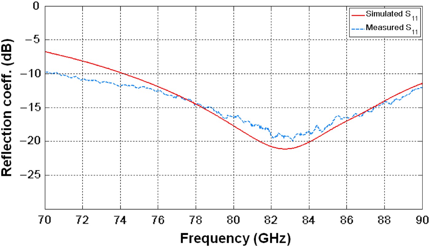
Fig. 9. Simulated and measured S11 for single slot antenna.
Measurements of the complete 8 × 8 antenna RX array have not been performed due to the complex measurement setup. Instead measurements have been made on single TX and RX 1 × 8 sub-arrays. The measured reflection and E-plane pattern are shown in Fig. 10. The measured reflection coefficient is better than 10 dB in the frequency range 70–90 GHz. The measured maximum gain is about 4.5 dBi at the frequency 79 GHz. The single 1 × 8 array measurements of the TX and RX antennas have similar behavior.

Fig. 10. Simulated and measured reflection coefficients of the RX sub-array and measured E-plane co-polarization of TX and RX array antennas at 79 GHz.
To improve radiation efficiency, suppress undesired parallel plate modes and suppress back radiation, a cavity back-short was assembled over the top-side of the TX and RX arrays, (Fig. 11). The measured maximum gain of the RX4 array antenna in the E-plane (using the cavity with no ribs), shown in Fig. 12, is approximately 6.6 dBi, which is roughly 2 dB higher than the corresponding measurement shown in Fig. 10. However, due to the presence of unwanted cavity modes, the backward radiation is quite large and there are strong ripples in the H-plane radiation patterns, (also shown in Fig. 12).

Fig. 11. Photo of antenna back-short cavity (no ribs and ribbed) and the antenna assembly.

Fig. 12. Measured E-plane and H-plane radiation patterns of the RX4 array antennas backed by a metal cavity.
The ribbed metal cavity (see Fig. 11) was used instead and measurements were repeated. The simulated and measured E- and H-plane radiation patterns of the RX4 array antenna are shown in Fig. 13. The back radiation is improved by more than 10 dB (compared to the corresponding measurements in Fig. 12) and smooth curves can be observed. The measured results indicate that the antenna exhibits a maximum gain of 6.6 dBi, E-plane side lobe suppression of 17 dB and back radiation of approximately −20 dBi.

Fig. 13. Simulated and measured E-plane and H-plane radiation patterns of the RX4 array antennas backed by a ribbed metal cavity.
Details and results regarding the complete antenna with cavity back-short assembly are provided in [Reference Pettersson, Cheng, Salter, Rydberg and Platt9].
VIII. LOW COST ASSEMBLY
For the GaAs MMIC-based demonstrator, a low-cost assembly process was developed together with UMS. The process is designed to be compatible with stud-bumped hot-via GaAs TX/RX MMICs and uses conductive adhesive and underfill for die attach to the thin-film substrate. The contact resistance from chip to substrate was measured over 21 contact points giving an average contact resistance of 470 mΩ. This value is compatible with good microwave performance and will induce only 0.04 dB of losses at millimeter-wave interconnects. Figure 14 shows the TX MMIC assembled onto the MCM-D Si BCB carrier. Details and results regarding the assembly process are provided in [Reference Alléaume, Toussain, Auvinet, Domnesque, Quentin and Camiade8].

Fig. 14. Photo of face-up hot-via GaAs MMICs on MCM-D substrate.
IX. MODULE DESIGN
The automotive radar demonstrator of Hi-Mission has been designed as two module variants, Charon and Pluto (see Figs 15 and 16). The Charon module is designed for conductive measurements (no embedded antenna) and allows for selective measurement and verification of individual sections of the modules. The VCO frequency doubler, VGA Mixer, and TX sections can all be verified independently by appropriate selection of wire-bond locations. The Pluto module is designed for radiated measurements using a corner reflector.

Fig. 15. Photos of the complete assembled Charon 79 GHz radar module.

Fig. 16. Photo of the complete assembled Pluto 79 GHz radar module.
X. RADAR DEMONSTRATOR ASSEMBLY AND PCB
The MCM-D module is epoxied and wire-bonded onto a PCB. The Pluto module Printed Circuit Board (PCB) has a square opening allowing for direct antenna radiation. An antenna back-short cavity can be assembled onto the Pluto module for enhanced performance (Fig. 17).

Fig. 17. Photo of the assembled Charon and Pluto module 79 GHz radar front-end demonstrators.
The PCB has the VCO stabilization and FMCW ramp generation, which is performed by a programmable direct digital synthesizer (DDS) and phase-locked loop (PLL). PLL stabilization of the VCO during frequency ramping is required in order to obtain the required frequency sweep linearity over time. Programming and communication with the DDS are performed by a USB micro-controller which in turn can be connected to a computer via a USB cable. The PCB also contains the power supplies and biasing for the MMICs on the MCM-D module as well as interfacing to the eight mixer outputs.
XI. RADAR DEMONSTRATOR TEST RESULTS
The VCO and PLL performance were measured using the Charon demonstrator. The PLL lock in range was measured to be 11.96–13.44 GHz (equivalent to 71.8–80.6 GHz at the TX output) that is in accordance with specifications. The PLL loop was observed to be stable for a 1 MHz step response for the PLL reference (equivalent to a 128 MHz step for the VCO).
The VCO phase noise was measured with the PLL locked at 12.8 GHz (see Fig. 18). The VCO phase noise result is slightly better than the values specified at 10 and 100 kHz. The FMCW ramp linearity was measured at the prescaler output to be 0.4% for a 3.8 GHz frequency ramp with period 150 µs (Fig. 19). The measurement excludes the error when the ramp changes direction.

Fig. 18. The VCO phase noise (PLL locked).

Fig. 19. FMCW sweep and frequency linearity.
The amplitude balance of the distribution network for the 39 GHz LO was measured to be <0.3 dB on both Charon and Pluto demonstrators. This demonstrates the accurate and repeatable behavior of integrated passive devices, interconnections and transmission lines implemented in the MCM-D substrate.
The Variable Gain Amplifier (VGA) gain and tuning range was measured to be 17.7 and 25 dB, respectively, in line with specification. The TX output was observed to be from 76.0 to 80.6 GHz. The gain of the X2 amplifier was measured to be approximately 13.4 dB and the TX output power level was measured (after calibrating losses) to be approximately 14 dBm, again in good agreement with specification.
It was beyond the scope of this project to create software to provide the signal processing necessary for the analysis and averaging of the combined eight mixer IF outputs from the RX antenna arrays and digital beam steering. Without such software it was not possible to achieve the Signal to Noise Ration (SNR) for the radar demonstrator. Therefore, it was only possible to analyze the output from one RX antenna array at a time. To do this, the output from a RX mixer on the Pluto demonstrator was amplified with an Low Noise Amplifier (LNA) before being input to a spectrum analyzer. The output was measured first without and then with FMCW ramping at a ramp period of 200 µs (Fig. 20). To demonstrate radar functionality a moving object (reflector) was applied and the output observed (Fig. 21).

Fig. 20. Measured output from mixer 1 via LNA on Pluto radar demonstrator without and with 200 µs FMCW sweep.

Fig. 21. Measured output from mixer 1 via LNA on Pluto radar demonstrator with 200 µs sweep and moving object.
The RX single channel noise level, with no ramp applied, is approximately −120 dBm. The antenna isolation between RX antenna arrays is measured to be >30 dB [Reference Pettersson, Cheng, Salter, Rydberg and Platt9] so the TX antenna to the RX antenna isolation should also be >30 dB. The 5 kHz periodic frequency spectrum output of Fig. 20 is caused by the 200 µs period FMCW LO mixed with the slightly delayed direct coupled FMCW signal from TX to RX. A moving object causes a clear Doppler frequency shift of the reflected FMCW signal by approximately 317 Hz (Fig. 21) corresponding to a detected speed of approximately 0.6/ms.
XII. CONCLUSIONS
The Hi-Mission project has developed a silicon-based millimeter-wave platform capable of wideband millimeter-wave frequency operation. The successful assembly and results obtained from the working automotive radar front-end demonstrator have shown the innovative technology, suitability and capability of the Hi-Mission silicon-based platform. The platform includes MCM-D substrate technology, hot-via interconnects, MMICs in GaAs or SiGe, integrated slot array antenna, integrated passive devices, and low cost assembly and packaging concepts. The technology platform is suitable for SoCs and SiPs working at millimeter-wave frequencies as well as for future 76–81 GHz automotive radar applications. It is envisioned that a single, all silicon, wideband automotive radar module with integrated phase shifting functionality for beam steering will allow for low-cost collision avoidance radar, bringing automotive safety to a wider market. The achievements made indicate that the Hi-Mission platform has the potential to provide competitive, low-cost millimeter-wave solutions.
ACKNOWLEDGEMENTS
The authors would like to thank their partners in the automotive radar demonstrator, UMS, Uppsala University and Volvo and all the sub-contractors that supported the project. They also extend their thanks to Ericsson Research for excellent leadership of the Hi-Mission project. The authors also thank the MEDEA+ for the approval, support and review of the project as well as the public authorities of Sweden, Vinnova, for financing the Hi-Mission project.
 Duncan Platt received his B.Sc. from the University of Strathclyde, Scotland, in 1986. He is a member of IEEE. He started his career working with optical and vibratory gyroscope technology development at the company formerly known as GEC Ferranti in Edinburgh, Scotland. In 1994, he joined Ericsson Telecom in Norrköping, Sweden, working as an electronic design engineer in the development of high data rate fiber-optic line terminal equipment. From 1997 to 2008, he was a consultant at the Swedish consultancy company ÅF, where, among other things, he was responsible for the hardware design of one of the world's first automotive safety telematic systems for Autoliv Electronics and Volvo. He is currently employed as a project manager in the Microelectronics group at the Swedish research institute Acreo AB in Norrköping, Sweden, where he is managing several applied research projects in the areas of microwave and millimeter wave front-end technology for radar, very high data communication rate, and security imaging applications.
 Lars Pettersson received the M.Sc. degree in microwave engineering from Chalmers University of Technology, 1998. He joined Ericsson Microwave Systems in 1998, Gothenburg, where he worked with communication links and GaAs MMIC development for radar modules. From 2002 to 2006 he worked at Autoliv Electronics, Linköping, Sweden, where he was engaged in designing antennas and RF electronics for the automotive industry. Lars is currently employed at Acreo AB in Norrköping, Sweden. His main interests are development of integrated antennas, radar front-ends and integrated circuits for microwave and millimeter wave frequencies.
 Darius Jakonis received the B.S. and M.S. degrees in physics and electronics in 1996 and 1998 from Vilnius University, Lithuania. During 1997–98, he worked as a telecommunication engineer at State Radio Frequency Service, Vilnius, Lithuania. In 2004, he received the Ph.D. degree in electrical engineering from Linköping University, Sweden. His research was focused on analog CMOS integrated circuits for signal sampling, down conversion, filtering, decimation, and A/D conversion. He was investigating new solutions for radio front-end applications, methods to reduce non-idealities in high-speed sampling, and readout architectures for un-cooled infrared detector arrays. In 2004, he joined Acreo AB in Norrköping, Sweden, as an IC designer. He is currently working on the development of sensor readout electronics and RF circuits for automotive radar application.
 Michael Salter has B.S. and M.S. Engineering degrees from the University of New Hampshire, USA and over 22 years of research, engineering, and management experience, both in USA and Europe. He is a member of IEEE. His career in the electronics field began with Ericsson Telecommunications in the areas of analog and mixed mode simulation for telecom switching infrastructure hardware. It continued with engineering and management positions at Motorola Personal Communications in the area of RF module, electronic packaging and components for CDMA and GSM cellular phones. At the Motorola Advanced Technology Centre, he managed a group of RF design and test engineers and led a large corporate wide program to introduce high density interconnect, or HDI, PCB technology into Motorola's first cellular phone transceiver. He currently manages the Microelectronics group at the Swedish research institute, Acreo AB in Norrköping, Sweden, where he leads research into advanced integration for high frequency and sensor applications.
 Joacim Haglund received the M.Sc. degree in applied physics in 1995 from Linköping Unviersity, Sweden. Until mid-2008, he was employed at the Swedish research institute Acreo AB in Norrköping, Sweden, working mainly with thin-film processes for interconnection and packaging of micro-optics and electronics. He is currently employed by HiQ Ace AB in Linköping.


