


I. INTRODUCTION
The implementation of radio frequency (RF) and microwave components (in microstrip or coplanar-waveguide technology) is typically based on the chemical etching of plastic or ceramic substrates, metalized on both the faces. This fabrication process is widely spread for several applications, as it is very practical and cost-effective. Nevertheless, this approach results in significant environmental impact, both during the fabrication of the components, and at the end of its operational life. The major reasons for this impact are the use of acids and heavy metals (especially copper) during the fabrication phase, and the substrate material to be dumped at the end of the operational life of the components. For these reasons, since a long time there is an open discussion about possible alternative fabrication techniques, aiming at reducing the environmental impact of electronic circuits fabrication [Reference Harrison, Billett and Billingsley1]. Among the proposed alternative solutions, the use of paper looks like an optimal candidate: in fact, paper is a widely available and extremely cheap material, and it is completely environmental friendly, both during its production and at the time of its dumping.
The use of paper for the implementation of RF and microwave components and antennas has been demonstrated in the last few years [Reference Tentzeris2–Reference Björninen, Merilampi, Ukkonen, Ruuskanen and Sydänheimo7]. The paper used for this application is commercially available and must have a hydrophobic coating. The thickness of a single paper layer is around 230 µm and multilayer configurations can be achieved by heat bonding [Reference Yang, Rida, Vyas and Tentzeris3]. The electromagnetic characteristics of paper have been measured in the frequency range up to a few GHz [Reference Yang, Rida, Vyas and Tentzeris3]. The manufacturing of paper-based components can be obtained by inkjet printing, with no need of chemical etching and use of acids. The procedure is quite straightforward: a special inkjet printer jets the single ink droplets from the nozzle to the desired position (usually ink with particles of silver is adopted, due to its high conductivity [Reference Björninen, Merilampi, Ukkonen, Ruuskanen and Sydänheimo7]). A metal thickness of 12 µm can be achieved with 12 ink layers [Reference Vyas4]. The fabrication process ends with the sintering, which is needed in order to make the ink droplets continuous and to increase the conductivity [Reference Yang, Rida, Vyas and Tentzeris3]. This procedure can yield a resolution of about 20 µm [Reference Tentzeris2], compatible with most of the microwave circuits. Antennas, radio frequency identification (RFID), and sensors have been implemented with this technique, in the frequency range up to 2.5 GHz [Reference Lakafosis, Rida, Vyas, Yang, Nikolaou and Tentzeris6, Reference Anagnostou, Gheethan, Amert and Whites8]. Furthermore, it is possible to realize metalized holes in the paper substrate [Reference Vyas4]: the procedure requires making the holes by a micro-drill, filling them with silver epoxy, and finally sintering the conductor ink. Active elements can be integrated on the paper substrate, by means of conductor tape, with proper heating and pressure [Reference Vyas4].
In this paper, the implementation of substrate-integrated waveguide (SIW) components and antennas on paper substrates is presented for the first time. SIW structures are similar to traditional rectangular waveguides, and are implemented in dielectric substrates by using two rows of metalized holes that connect the two ground planes of the substrate [Reference Deslandes and Wu9]. SIW technology represents an emerging approach for the development of microwave and millimeter-wave components in planar form [Reference Bozzi, Georgiadis and Wu10]. It allows integrating all components on the same substrate including passive structures, active components, and antennas, according to the system-on-substrate (SoS) approach [Reference Wu11]. SIW technology combines the advantages of classical microstrip circuits (low cost, easy fabrication, compact size, and low weight) and metallic waveguides (low losses, complete shielding, and high-power handling capability).
Paper-based fabrication appears very suitable for the realization of SIW components, as it allows for arbitrary geometry, conformal shape, and multilayered configuration, thus fully exploiting the design flexibility of SIW technology. The use of paper substrate increases the advantages of SIW components: flexible and environmental friendly dielectric substrates are investigated with growing interest for a variety of wireless systems and wearable applications. Moreover, the possibility of manufacturing multilayered configurations permits to reduce appreciably the size of components, as well as to obtain multi-functional components integrated in a single structure.
The implementation of SIW components on paper substrate is suitable for several wireless applications. The most significant application is in wireless sensor networks (WSNs), which consists of spatially distributed autonomous sensors that permit the remote monitoring of physical quantities or environmental conditions (temperature, humidity, pressure, concentration of pollutants, etc.). The most important advantage of using paper, for this kind of applications, is the possibility to deploy a large number of sensors without any environmental drawback. In fact, the eco-friendly features of paper substrate and inkjet-printing fabrication process permit to limit the environmental impact of the sensor networks. Furthermore, the use of extremely cheap substrates allows reducing the cost of the sensor nodes and, consequently, the cost of the whole system; more and more sensors can be distributed to monitor physical quantities with a good level of efficiency and accuracy.
The nodes of a WSN should exhibit a small size, in order to cut down the losses and the cost of components. In order to reach this goal, a fundamental aspect is the dense integration in a single substrate of the complete circuit (including sensors, microprocessor, antennas, and possibly the energy-harvesting system). The SIW approach, together with the implementation of multi-layered configurations, can help to achieve this target. Therefore, the SIW technology in conjunction with paper substrate perfectly meets the requirements for the implementation of sensor node for WSN. Moreover, paper-based SIW components and systems can be developed not only for WSNs, but also for other wireless applications, such as the future Internet of Things (IoT), whose implementation needs thousands or millions of small and cost-effective wireless sensor nodes.
II. INKJET PRINTING, VIA AND FABRICATION PROCESS
Inkjet-printing technology is utilized in this work to fabricate SIW structures on the paper substrate. The inkjet printing has a couple of advantages compared to the conventional fabrication methods. It does not produce any byproducts and it is cost-effective and environmental friendly [Reference Lakafosis, Rida, Vyas, Yang, Nikolaou and Tentzeris6]. The paper substrate is also environmental friendly and renewable organic material. In addition, it is one of the cheapest materials in the world and easy to process also.
A paper substrate for high-frequency application such as SIW has lots of advantages. Mass production is feasible when it is combined with roll-to-roll inkjet-printing technology, which is enabling to reduce fabrication cost.
A) Inkjet printing on paper substrate
The paper substrate is one of the cheapest materials as well as renewable and biocompatible materials. The high-frequency characteristics of the paper substrate are studied using the microstrip resonators [Reference Yang, Rida, Vyas and Tentzeris3, Reference Cook and Shamim12]. The reported electromagnetic characteristics of a 228.6-μm-thick Kodak photo paper are the dielectric constant (ε r) in the range of 2.8–3.1 and the loss tangent (tan δ) in the range of 0.055–0.065 at 1–10 GHz.
For the inkjet-printing process, the Dimatix DMP2800 drop on demand (DOD)-type inkjet printer [13] and the Dimatix 10 pL cartridge (DMC-11610) were utilized. The angle of the printer head was set to 4.5° in order to achieve a printing resolution of 1270 dpi (dots per inch). Cabot CCI-300 silver nano-particle ink was used for printing, which has viscosity of 11.6–13 cP and surface tension of 28.0–31.0 dynes/cm [14]. The nozzle and the substrate temperatures were kept at 36.5 and 50°C, respectively. The printed pattern was sintered in the thermal oven at 130°C for 4 h after printing of five layers. This sintering process is very important to increase conductivity of the printed patterns because solvents and impurities can be removed during this process. The printed patterns on paper substrate usually have a DC conductivity in the range of 9 × 10⁶–1.1 × 10⁷ S/m with roughness of about 1 µm [Reference Kim, Ren, Lee, Rida, Nikolaou and Tentzeris15].
B) Via fabrication on paper substrate
Concerning the via fabrication, there are many methods to make via hole such as chemical etching, laser processing, and drilling [Reference Lehmann16–Reference Polyakov18]. The drilling and laser processing are suitable processing for the paper substrate because those are complete dry processing and no surface treatment is required. In addition, those processes have very good aspect ratios and feature sizes. The aspect ratios of drilling and laser processing are larger than 10 and 20, respectively. The general achievable feature size of drilling is 300 µm and of laser processing is 5 µm [Reference Polyakov18].
In this paper, drilling is utilized to make via holes since it does not damage the substrate and the rim of via holes. Some blackening is observed around via hole when the laser processing is utilized. This may degrade the performance of the inkjet-printed circuits on paper substrate, since the electric properties of the burnt area are different from their original properties.
For the via hole metallization, cylindrical copper rivets are utilized. In previous works, via holes were metalized using conductive epoxy or printing conductive ink over and over [Reference Rida, Vyas, Yang, Kruesi and Tentzeris19, Reference Reinhold, Thielen, Voit, Zapka, Gotzen and Bohlmann20]. The epoxy filled via hole cannot guarantee the tight contact to side wall of the via hole, nor the roughness of the metalized via hole. The ink-filling technique cannot be applied to thick substrates, and in the case of paper substrate it appears critical, since paper absorbs ink during the printing process. For achieving a repeatable and stable via hole metallization, a cylindrical copper rivet with outer diameter of 0.8 mm is inserted into the via hole.
C) Fabrication process
The whole fabrication process is depicted in Fig. 1. For the first step, the SIW structure is printed on the single layer of paper substrate. Two more layers of paper substrate are stacked to get the desired substrate thickness of 0.69 mm after sintering the printed pattern. The PolyVinylPyrrolidone (PVP)-based glue is utilized to bond the paper substrates because of ease of fabrication and its electrical permeability is very close to that of the paper [Reference Lolli21]. The copper ground plane is bonded, and via array is drilled. The top and bottom of the via hole are covered with conductive epoxy or soldering to improve the contacts after filling the via holes with the cylindrical copper rivets.

Fig. 1. Different steps of the fabrication process of SIW components on paper substrate. (a) Inkjet print the pattern; (b) Stacking the substrate after sintering; (c) Drilling via holes; (d) Insert rivets; (e) Encapsulate.
III. PAPER-BASED SIW COMPONENTS
A variety of SIW interconnects and components have been designed and fabricated, to verify and show the applicability of inkjet-printing technology to this class of circuits.
A) SIW interconnects
As a first step, straight SIW interconnects on paper have been implemented. The SIW lines have been designed for operation frequency of 5 GHz, and for this reason the cutoff frequency of the fundamental mode was set to f 0 = 3.75 GHz. This performance is achieved by properly selecting the geometrical dimensions of the SIW structure (Fig. 2): the width of the SIW is w = 24 mm, the diameter of metal vias is d = 0.8 mm and their longitudinal spacing is s = 1.6 mm. The dimensions of the pitch and the diameter of the holes were chosen, on the one hand, to avoid the radiation leakage and, on the other hand, to minimize the fabrication inaccuracy. According to [Reference Xu and Wu22], the radiation leakage is very limited for s < 2.5 d, and negligible for s = 2d.

Fig. 2. Geometry of an SIW interconnect on paper.
The substrate thickness is approximately 0.69 mm, which is obtained by stacking three layers of paper (each of them with a thickness of 0.23 mm). As conductor loss can be minimized by increasing the substrate thickness [Reference Bozzi, Georgiadis and Wu10], this thickness has been chosen reasonably large to reduce the loss component due to the relative low ink conductivity. The structures have been designed, considering the nominal relative values of the dielectric permittivity ɛ r = 3, the loss tangent tan δ = 0.06, and the ink conductivity σ = 1.5 × 10⁷ S/m.
The design of SIW structures has been performed by using the full-wave electromagnetic simulator Ansys HFSS. The design of the SIW interconnects includes the transitions from 50-Ω microstrip line to SIW to allow the experimental characterization.
Three transmission lines with different length have been fabricated, with the aim to determine the dispersion curve of the SIW interconnect and to extract the electrical parameters of paper substrate. The three transmission lines have a length of 13, 20, and 27 unit cells, respectively, each unit cell consisting of a waveguide section with two metalized holes, as shown in Fig. 2. The photographs of the three prototypes are shown in Fig. 3.

Fig. 3. Photograph of the prototypes of three SIW interconnects with different length.
The scattering parameters of the three SIW structures have been experimentally determined. The comparison between simulations and measurements is reported in Fig. 4, in the case of the shortest interconnect. Moreover, the propagation constant of the SIW fundamental mode has been derived, by comparing the measured scattering parameters of two SIW interconnects with different length, according to the method described in [Reference Xu and Wu23]. The simulated and measured values of the propagation constant versus frequency are shown in Fig. 5. The small discrepancies between theory and measured data are attributed to repeatability issues in the fabrication of different SIW interconnects. In particular the difference near the cutoff frequency is attributed to the radiated coupling between the microstrip-to-SIW transitions. In fact, a small portion of the power radiated by the transition is received by the other one.

Fig. 4. Simulated and measured scattering parameters of an SIW interconnect on paper.

Fig. 5. Simulated and measured propagation constant of the SIW interconnects on paper.
The measured dispersion curve also permits to derive the relative dielectric constant of the paper substrate, which is shown in Fig. 6. The estimated value of the relative dielectric constant is ɛ r = 2.85 over the entire frequency band of interest, very close to the nominal value. In addition, the attenuation was estimated: the insertion loss of the SIW is 0.5 dB/cm at 5 GHz, while each microstrip-to-SIW transition and connector introduces an additional attenuation of approximately 0.5 dB.

Fig. 6. Experimentally derived value of the relative dielectric constant of the paper substrate.
B) SIW cavity filter
A two-pole SIW filter has been designed, fabricated and measured, to investigate the feasibility and performance of SIW components on paper substrate. The topology of this filter is very simple: it comprises two cavities, connected by an iris-coupling aperture, and the dimensions are optimized for band-pass operation around 5 GHz.
The layout of proposed filter is illustrated in Fig. 7: the geometry of the SIW and of the transitions is the same as in the case of the straight interconnects, whereas new posts have been added to define the two cavities. A photograph of the prototype is shown in Fig. 8.

Fig. 7. Geometry of the SIW filter on paper (w = 24 mm, a = 14.27 mm, b = 15.89 mm, and l = 19.17 mm).
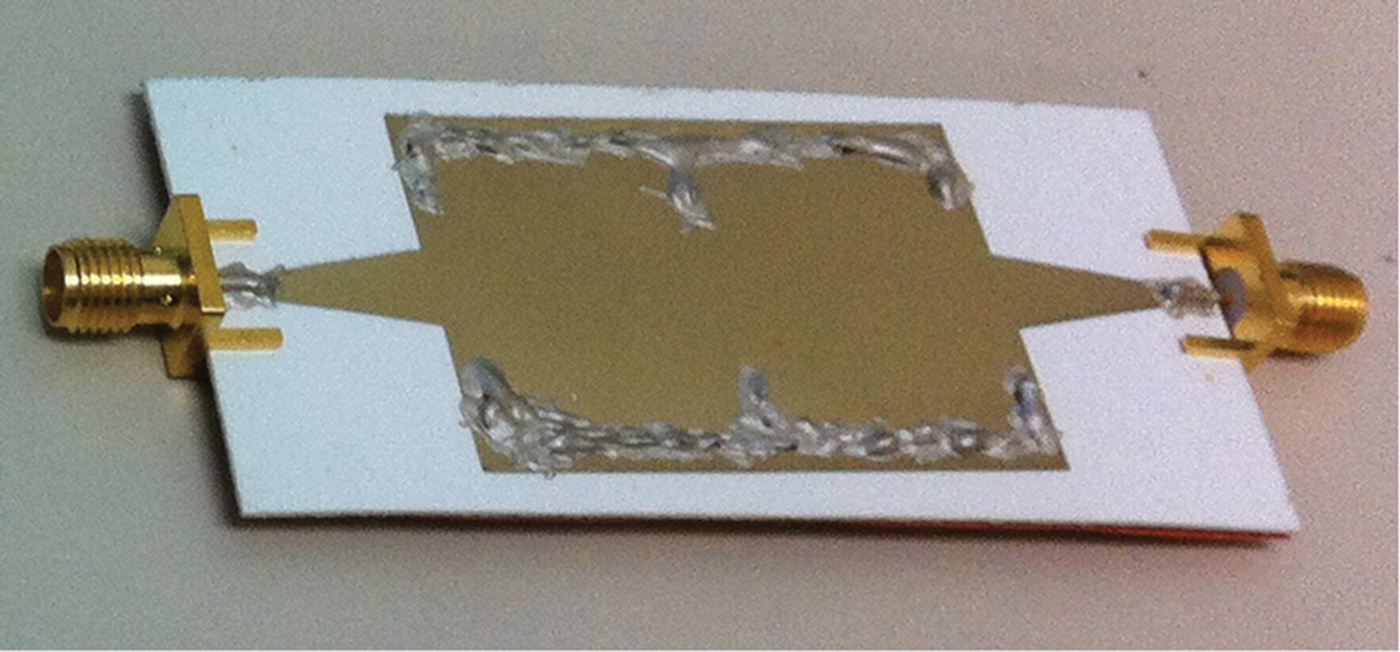
Fig. 8. Photograph of the SIW filter on paper.
The simulated and measured frequency response of the component is reported in Fig. 9, with a measured insertion loss of approximately 5 dB at 5 GHz.

Fig. 9. Simulated and measured scattering parameters of the SIW filter on paper.
These results show that losses represent an issue, and the performance of the filter is affected by the significant losses of the material. For this reason, the filter topology needs to be carefully selected for the effective implementation of SIW filters on paper. Possibly, the use of pre-distorted filter configurations could represent an interesting solution and partially mitigate this issue [Reference Mira, Mateu and Bozzi24].
IV. PAPER-BASED SIW ANTENNAS
A paper-based slotted-waveguide SIW antenna has been designed and optimized at the central frequency of 5.6 GHz. The layout of the antenna is shown in Fig. 10. The antenna consists of an SIW structure with four longitudinal resonant slots, alternatively located with respect to the middle on the top metal wall of a straight SIW structure. The length of the slots has been selected to resonate at the design frequency of 5.6 GHz, and their longitudinal spacing is approximately half-guided wavelength in order to obtain maximum radiation in the broadside direction. This SIW antenna topology appears to be robust versus small bending of the dielectric substrate, as shown in [Reference Moro, Collado, Via, Georgiadis and Bozzi25]. In addition, this kind of antenna exhibits linear polarization, with good performance in terms of polarization purity.

Fig. 10. Geometry of SIW slotted-waveguide antenna on paper.
Differently from the usual configuration of slotted-waveguide antennas, the end section of the SIW is not short-circuited: in the design of this SIW antenna, the end of waveguide is closed by a matched load. This solution permits to improve the input matching of the antenna on a broader bandwidth without decreasing the radiation efficiency. The load is realized by means of SIW-to-microstrip transition ended with a 50-Ω matching resistor, connected to the ground plane thanks to a metalized via hole (Fig. 10).
The length and the width of each slot are 17 and 1.15 mm, respectively. The longitudinal spacing of the slots results 25.5 mm and their offset with respect to the center of the waveguide is 1.2 mm. The optimized parameters of the matched load are: L t = 6 mm, W t = 15 mm, W r = 0.8 mm, L r = 1.6 mm, and L s = 1 mm. A picture of the prototype is shown in Fig. 11.

Fig. 11. Pictures of the prototype of the paper-based SIW slotted-waveguide antenna: (a) front side, showing the microstrip-to-SIW transition, the slots and the matched load; (b) back side, showing the conductive epoxy adopted to guarantee a good ohmic contact of the vias.
The simulated and measured input matching of the SIW slot array antenna are shown in Fig. 12. The return loss is higher than 10 dB within a relative bandwidth of 20% (approximately 1.15 GHz bandwidth around the central frequency of 5.6 GHz). According to simulations, the matched load absorbs 3.7% of the available power at the central frequency of 5.6 GHz.

Fig. 12. Simulated and measured scattering parameters of the SIW antenna on paper.
The radiation performance of the SIW antenna was experimentally determined in an anechoic chamber: the radiation pattern of the antenna, in both the E- and H-planes, was measured at 5.6 GHz. Figure 13 shows a very good agreement of simulated and measured radiation patterns in the E-plane. Conversely, in the H-plane the measured results exhibit some discrepancies compared to the simulations, which was attributed to the presence of the feeding system and cables. Finally, Fig. 14 shows the gain of the antenna in the broadside direction versus frequency. The measured radiation efficiency at the resonant frequency is 5.8%, which agrees well with the simulated result. The limited value of radiation efficiency is mainly attributed to the dielectric loss, which reduces the radiated power.

Fig. 13. Simulated and measured radiation patterns of the slotted-waveguide antenna SIW: (a) E-plane radiation pattern; (b) H-plane radiation pattern

Fig. 14. Simulated and measured broadside gain of the slotted-waveguide SIW antenna.
V. CONCLUSION
SIW interconnects, components, and antennas have been implemented by inkjet printing on paper substrate for the first time. The design and the steps of the fabrication process have been described. Straight interconnects, a filter, and a slotted-waveguide antenna have been fabricated and tested, demonstrating the applicability of paper-based technology to SIW structures.
While the achievable performance of paper-based SIW components is still inferior to components based on commonly used dielectric material, the implementation of SIW structures on paper substrate represents a significant step: it is the groundwork for future wireless systems and wearable devices, as it combines the advantages of low-cost, flexible and environmental friendly material with the integration potential of SIW technology. Wearable systems implemented by inkjet printing on the paper substrate could perfectly complement the use of textile-based wireless systems [Reference Moro, Agneessens, Rogier and Bozzi26], for instance in health applications like smart plasters, where the direct contact with skin is required.
According to the current performance of paper substrates, the feasibility of paper-based SIW components beyond the frequency of 10 GHz is expected. An extension to a much higher frequency could be limited by large dielectric loss.
 Riccardo Moro received the M.S. degree in Electronic Engineering from the University of Pavia, Italy, in 2010. In November 2010, he joined the Department of Electronics of the University of Pavia as a Ph.D. student in Electronics. His research activities are focused on the implementation of radio systems in substrate-integrated waveguide (SIW) technology based on innovative eco-friendly materials.
 Sangkil Kim received the B.S. degree in electrical and electronic engineering from Yonsei University, Seoul, Korea, in 2010, and the M.S. in electrical engineering from Georgia Institute of Technology, Atlanta, GA, in 2012. He is currently pursuing his Ph.D. degree at Georgia Institute of Technology, Atlanta, GA, in 2013. He is currently working on inkjet-printed wearable electronics for body area networks.
 Maurizio Bozzi was born in Voghera, Italy, in 1971. He received the M.S. degree in Electronic Engineering and the Ph.D. in Electronics and Computer Science from the University of Pavia, Italy, in 1996 and 2000, respectively. In 2002, he joined the Department of Electronics of the University of Pavia as an Assistant Professor. He held research positions with various universities worldwide, including the Technische Universitaet Darmstadt, Germany, the Universitat de Valencia, Spain, and the École Polytechnique de Montréal, Canada. His main research activities concern the development of numerical methods for the electromagnetic modeling of microwave and millimeter-wave components. He was the general chair of the IEEE MTT-S International Microwave Workshop Series on Millimeter-Wave Integration Technologies (2011) and the Guest Editor of the Special Issue “RF/Microwave Communication Subsystems for Emerging Wireless Technologies” in the IET Microwaves, Antennas & Propagation (2011). Professor Bozzi co-authored the book “Microstrip Lines and Slotlines” (Artech House, 2013).
 Manos M. Tentzeris received the Diploma Degree in Electrical and Computer Engineering from the National Technical University of Athens in Greece and the M.S. and Ph.D. degrees in Electrical Engineering and Computer Science from the University of Michigan, Ann Arbor, MI. He is currently a Professor with School of ECE, Georgia Tech, Atlanta, GA. He has helped develop academic programs in Highly Integrated/Multilayer Packaging for RF and Wireless Applications using ceramic and organic flexible materials, paper-based RFID's and sensors, biosensors, wearable electronics, inkjet-printed electronics, “Green” electronics and power scavenging, nanotechnology applications in RF, Microwave MEM's, SOP-integrated antennas, and Adaptive Numerical Electromagnetics. He is a Fellow of IEEE, a member of MTT-15 Committee, an Associate Member of EuMA, a Fellow of the Electromagnetic Academy, and a member of the Technical Chamber of Greece. Professor Tentzeris was one of the IEEE MTT-S Distinguished Microwave Lecturers (2010–2012).


