


Introduction
In the last years, the advent of the Internet of Things (IoT) [Reference Giusto, Iera, Morabito and Atzori1–3] and, more recently, of the fifth generation of mobile networks (5G) [Reference Rappaport, Sun, Mayzus, Zhao, Azar, Wang, Wong, Schulz, Samimi and Gutierrez4, Reference Boccardi, Heath, Lozano, Marzetta and Popovski5] is bound to change the scenario of wireless components and systems. In fact, the development of a variety of new applications in the microwave and millimeter-wave frequency range requires the implementation of a novel class of circuits, able to integrate data transmission, wireless power transfer, and sensing capabilities in a single wireless device. The success of these new applications relies on the several concurrent features: on the one hand, it is fundamental to identify a technology that guarantees high performance and, at the same time, low cost for mass production. Moreover, compact size and system miniaturization are becoming increasingly important, with the aim to develop seamless systems for wearable and low-impact applications. Finally, the constraints of a short time-to-market impose the choice of easy manufacturing processes and effective integration technologies.
Among the available implementation technologies that are good candidates for the development of future IoT and 5G systems, the substrate integrated waveguide (SIW) plays a key role [Reference Bozzi, Georgiadis and Wu6, Reference Garg, Bahl and Bozzi7]. The SIW is a waveguide-like structure, based on a dielectric substrate laminated with metal layers at both faces, where metal vias define the side walls of the waveguide. The major advantages of SIW technology are the easy design and manufacturing, the low losses, and the complete shielding. In addition, SIW structures can be conveniently integrated with classical planar technologies (e.g. microstrip lines and coplanar waveguides), as well as with active devices and microwave monolithically integrated circuits. A large variety of microwave and millimeter-wave SIW components have been implemented in the last 15 years, ranging from interconnects [Reference Deslandes and Wu8, Reference Bozzi, Deslandes, Arcioni, Perregrini, Wu and Conciauro9] and filters [Reference Chen and Wu10, Reference Delmonte, Silvestri, Bozzi and Perregrini11] to active antennas [Reference Giuppi, Georgiadis, Collado, Bozzi and Perregrini12, Reference Giuppi, Collado, Georgiadis and Bozzi13]. Moreover, SIW technology allows integrating a complete system in a single dielectric substrate, according to the system-on-substrate paradigm [Reference Li and Wu14]: this approach permits to avoid any transition between components developed by using different technologies, thus reducing losses and complexity.
Cavity-backed antennas represent a very interesting class of SIW radiating structures. In fact, they are easy to combine and integrate with the microwave circuitry, for instance to obtain antenna oscillators [Reference Giuppi, Collado, Georgiadis and Bozzi13], where the operation frequency can be tuned by adopting varactor diodes [Reference Giuppi, Georgiadis, Collado, Bozzi and Perregrini12]. Moreover, they are particularly suitable to wearable applications, as they can be simply integrated in clothes, and compared to patch antennas, they are relatively insensitive to on-body operation [Reference Moro, Agneessens, Rogier, Dierck and Bozzi15]. Several works have been published on cavity-backed SIW antennas [Reference Luo, Hu, Dong and Sun16–Reference Yusuf and Gong21]. One of the major limitations of these antennas is the small operation bandwidth, which depends on their intrinsic feature of being a resonant cavity with a small radiating aperture.
Besides, other antenna designs that adopt multiple coupled resonant elements to increase bandwidth are possible, for instance stacked patch antennas. The use of parasitic patches to increase antenna bandwidth was proposed in several papers [Reference Sung22, Reference Dubost, Beauquet, Rocquencourt and Bonnet23]. A recent work [Reference Klionovski and Shamim24] provided a design strategy for physically connected prototypes with 100% bandwidth. Despite of this interesting feature, patch antennas do not exhibit the advantages of SIW antennas, as previously emphasized.
This paper presents a technique to enhance the bandwidth performance of cavity-backed SIW antennas. The presence of the resonant cavity, which represents the reason of the intrinsic narrow-band operation, is exploited to increase the bandwidth, by adopting an approach inspired by the design of cavity filters. In fact, by adding more cavities, filters with more transmission poles can be obtained. Similarly, by connecting more cavities, the bandwidth of SIW cavity-backed antennas can be increased.
This work is organized as follows: after introducing the standard configuration for cavity-backed SIW antennas with single and double substrate thickness (sections “Design of single thickness cavity-backed SIW antenna” and “Design of double thickness cavity-backed SIW antenna”, respectively), the new two-cavity SIW antenna is presented in section “Two-cavity SIW antenna”. Simulations are compared with experimental results for all three antenna topologies.
Standard cavity-backed SIW antennas
This section presents the design of two standard cavity-backed SIW antennas: the former antenna consists of a rectangular SIW cavity, with a microstrip line with two deep insets on one side and a radiating rectangular slot on the other side, implemented on a substrate with thickness h = 0.76 mm (Fig. 1). The latter antenna is similar to the previous one except for the substrate height that is doubled (2h = 1.52 mm). The antennas have been designed by using the commercial software Ansys HFSS, to operate around the central frequency f 0 = 4 GHz, and to maximize the 10 dB input matching bandwidth. The dielectric substrate used for both antennas is Taconic TLX-9, with layer thickness h = 0.76 mm, relative permittivity ε r = 2.5, and loss tangent tanδ = 0.0022.
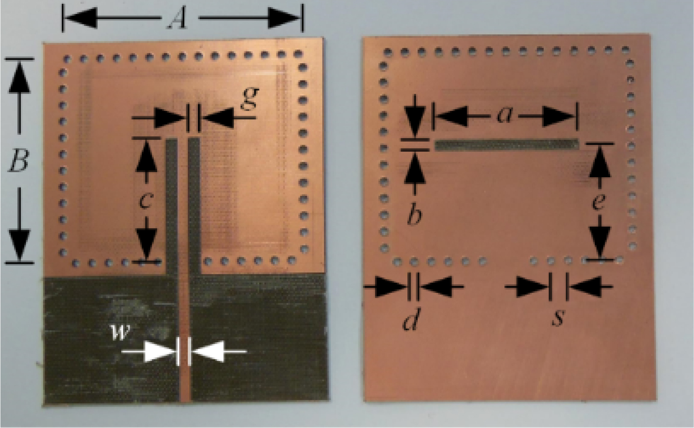
Fig. 1. Standard cavity-backed SIW antenna with substrate thickness h = 0.76 mm: photographs of the antenna feeding side (left) and of the radiating side (right).
Design of single thickness cavity-backed SIW antenna
The design of the standard cavity-backed SIW antenna with substrate thickness h is presented first, to provide a reference for the subsequent evaluation of the bandwidth enhancement.
The optimized antenna has cavity dimensions A = 39 mm and B = 38 mm (Fig. 1), the diameter of each metal via is d = 1.5 mm and the relative spacing between them is s = 3 mm, to avoid radiation leakage through the gaps [Reference Bozzi, Georgiadis and Wu6]. The cavity is fed by a 50 Ω microstrip line, characterized by the width w = 2.1 mm and the parameters g = 1.8 mm and c = 22 mm. On the radiating side (right part of Fig. 1), the rectangular radiating slot has dimensions a = 28 mm and b = 2.5 mm, and is shifted of an offset e = 20.7 mm from the lower row of metal posts. By adopting these dimensions, the antenna operates with the TM 120 mode (referred to z, that is the direction of maximum radiation of the antenna) of the resonant cavity, as shown in Fig. 2.
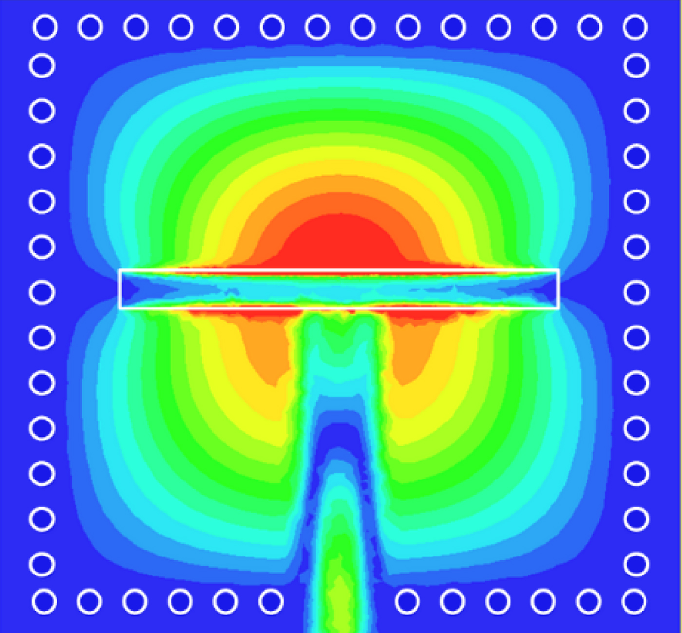
Fig. 2. Standard cavity-backed SIW antenna with substrate thickness h: amplitude of the electric field of the TM 120 mode, resonating in the cavity at the frequency of 4 GHz.
Simulation results of the antenna are shown in Fig. 3 (black solid lines). The simulated antenna exhibits a bandwidth (defined as |S 11| < −10 dB) of 60 MHz (Fig. 3(a)) and a boresight gain of 3.24 dB at the frequency of 4.04 GHz (Fig. 3(b)), corresponding to an antenna efficiency of 71%.

Fig. 3. Simulation and measurement of the standard cavity-backed SIW antenna with substrate thickness h: (a) simulated and measured scattering parameter |S 11| versus frequency; (b) simulated and measured gain versus frequency.
To validate the simulation results, a prototype has been fabricated by using a LPKF ProtoMat E33 milling machine for defining the pattern of the top and bottom metal layers and to drill the via holes. Subsequently, the lateral vias have been metalized with the LPKF ProConduct conductive paste. The photographs of the antenna feeding side and of the radiating side of the prototype are shown in Fig. 1.
The input matching and the boresight gain of the antenna have been measured in an anechoic chamber. The measured results are reported in Fig. 3 (gray dashed lines). More specifically, the measured values of the scattering parameter |S 11| versus frequency are shown in Fig. 3(a): the measured antenna bandwidth results 65 MHz (compared with 60 MHz from the simulations). In addition, Fig. 3(b) reports measured antenna gain versus frequency: the measured maximum gain is 3.64 dB at the frequency of 4.02 GHz.
Design of double thickness cavity-backed SIW antenna
A common technique to broaden the operation bandwidth of cavity-backed SIW antennas consists of increasing the thickness of the dielectric substrate. For this reason, a second antenna has been implemented, similar to the previous one but with double substrate thickness (2h = 1.52 mm). The optimized dimensions for this configuration are A = 39.1 mm, B = 37.8 mm, w = 4 mm, a = 30 mm, b = 2.5 mm, g = 1.9 mm, c = 22 mm, d = 1.5 mm, and s = 3 mm (see Fig. 1).
Similarly to the previous antenna, simulated scattering parameters |S 11| versus frequency are presented in Fig. 4(a) (black solid lines) around the frequency f 0 = 4 GHz. In this case, the simulated bandwidth (|S 11| < −10 dB) resulted 77 MHz. Therefore, as expected, a small benefit in terms of bandwidth increase can be achieved by doubling the substrate thickness. The simulated antenna gain versus frequency is reported in Fig. 4(b) (black solid lines), showing a boresight gain of 3.83 dB at the frequency of 4.03 GHz, corresponding to an antenna efficiency of 85%.

Fig. 4. Simulation and measurement of the standard cavity-backed SIW antenna with substrate thickness 2h: (a) simulated and measured scattering parameter |S 11| versus frequency; (b) simulated and measured gain versus frequency.
The antenna has been manufactured by gluing two layers of Taconic TLX-9, where unnecessary metal faces have been removed by chemical etching.
The measured scattering parameters |S 11| versus frequency are shown in Fig. 4(a) (gray dashed lines), providing a bandwidth of 71 MHz (compared with 77 MHz from the simulations). Moreover, the measured antenna gain versus frequency is shown in Fig. 4(b), and the maximum measured gain is 2.85 dB at the frequency of 4.02 GHz. A discrepancy between measured and simulated gain is observed in Fig. 4(b), which is attributed to a problem in the fabrication of the prototype, mainly due to a misalignment of the two layers.
Two-cavity SIW antenna
A significant bandwidth enhancement can be achieved by using an antenna topology with two stacked cavities (Fig. 5(a)). The idea is inspired by the cavity filters, which comprise resonant cavities properly coupled through apertures. Each cavity allows to place one pole in the frequency response of the filter, thus permitting to tailor the pass band.
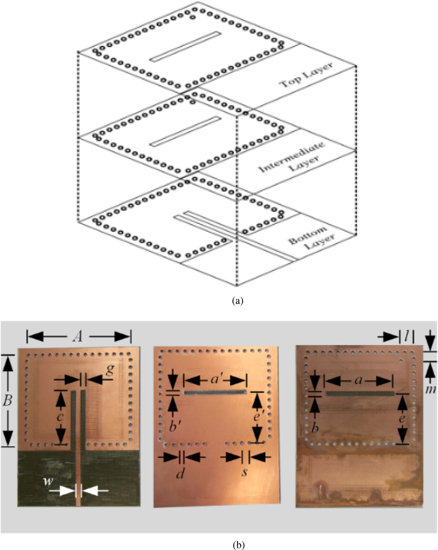
Fig. 5. Two-cavity SIW antenna: (a) 3D view of the structure (three overlapped metal layers); (b) photographs of the antenna bottom layer (left side), intermediate layer (center), and top layer (right side).
As shown in Fig. 5(a), a microstrip line in the bottom metal layer feeds the first (lower) cavity, and a slot in the intermediate metal layer couples the two cavities. Finally, another slot in the top metal layer allows radiation from the second (upper) cavity. In the proposed design, the two cavities have the same size and are located one on top of the other, in such a way that the metal vias of the two cavities are aligned. This assumption simplifies the fabrication process.
The antenna is implemented by using two layers of Taconic TLX-9, each of them with thickness h = 0.76 mm. The optimized antenna has cavity dimensions A = 43.65 mm and B = 37.78 mm, whereas d = 1.5 mm and s = 3 mm. In the bottom metal plane, the microstrip line has w = 2.1 mm, g = 2 mm, and c = 22.1 mm. In the intermediate metal plane, the rectangular slot coupling the two cavities has dimensions a′ = 29 mm, b′ = 2.14 mm, and the offset from the side wall is e′ = 22.4 mm. Finally, in the top metal plane, the radiating rectangular slot has a = 28 mm, b = 2.37 mm, and the offset is e = 22.9 mm. In addition, a perturbation post has been used in the upper cavity (with l = 4.8 mm and m = 3.5 mm), in order to tune the resonance frequency of the upper cavity and optimize the frequency response of the antenna, while keeping the same size for both upper and lower cavities.
Simulation results of the two-cavity SIW antenna are shown in Fig. 6 (black solid lines). The simulated antenna exhibits a bandwidth (|S 11| < −10 dB) of 120 MHz (Fig. 6(a)), which is significantly larger than the value achieved with the standard SIW cavity-backed antenna (with both single and double thickness). The boresight gain is 3.92 dB at the frequency of 4.02 GHz (Fig. 6(b)), corresponding to an antenna efficiency of 81%.

Fig. 6. Simulation and measurement of the two-cavity SIW antenna: (a) simulated and measured scattering parameter |S 11| versus frequency; (b) simulated and measured gain versus frequency.
To validate the design, this antenna has been fabricated by using the same technique previously adopted for the other antennas. The pictures of the prototype are shown in Fig. 5(b). Measured results for the scattering parameter |S 11| are reported in Fig. 6(a) (gray dashed line), showing a bandwidth of 150 MHz (120 MHz in the simulation). The measured gain versus frequency is provided in Fig. 6(b): the measured maximum gain is 4.42 dB at the frequency of 4.03 GHz.
To better understand the operation principle of the two-cavity SIW antenna, the amplitude of the electric field in the antenna is sketched in Fig. 7, in the ideal case of lossless materials and no radiation loss. At the frequency of 3.95 GHz, corresponding to the first pole of the frequency response, the TM 120 modes in the top and bottom cavities resonate out of phase (Fig. 7(a)). Conversely, at the frequency of 4.03 GHz, corresponding to the second pole of the frequency response, the TM 120 modes in the top and bottom cavities resonate in phase (Fig. 7(b)). This effect clearly relates the operation principle of the proposed antenna with the typical behavior of cavity filters.

Fig. 7. Amplitude of the electric field in the two-cavity SIW antenna (side view): (a) at the frequency of 3.95 GHz, corresponding to the first pole; (b) at the frequency of 4.03 GHz, corresponding to the second pole.
In conclusion, the comparison of the three antennas is reported in Table 1: while simulated and measured values for the antenna bandwidth are always in reasonable agreement, the solution based on two stacked cavities exhibits outstanding performance.
Table 1. Simulated and measured bandwidth for the three antennas

Conclusion
A novel cavity-backed antenna with enhanced bandwidth has been proposed. The antenna consists of two stacked SIW cavities, coupled through a slot, and has been implemented by using two dielectric layers with identical thickness h. The novel antenna as well as two standard structures have been fabricated and tested to demonstrate the bandwidth improvement. While the proposed antenna maintain a low profile and small footprint, it exhibits outstanding bandwidth performance over standard cavity-backed SIW antennas, both with thickness h and 2h (150 MHz instead of 65 and 71 MHz). The proposed solution, inspired by the design of cavity filters, can be potentially extended to a higher number of cavities, to further improve the antenna bandwidth.
 Hiba Abdel Ali is an electromagnetic/RF specialist and has over 7 years experience in solving antenna and microwave component-related problems. She holds a Ph.D. in Electronic and RF Systems Analysis in High Frequency from the Faculté des Sciences de Tunis, Université de Tunis El Manar, in May 2017, where she investigated the characterization of eco-friendly, low-cost, light-weight, and flexible substrates based on reflection methods up to 6 GHz, and developed techniques for enhancing the bandwidth, gain, and radiation efficiency of ultra-wideband antennas. In cooperation with the University of Pavia, Italy, she developed cost-effective and innovative eco-friendly manufacturing processes using flexible and ecological materials for the test and measurement of antennas and band-pass filters in ultra-wideband applications. Dr. Abdelali won the Student Challenge competition award at the EuMW Conference 2014 held in Rome, Italy, and won the best third paper in the IDT 2016 Conference held in Hamamet, Tunisia.
 Enrico Massoni was born in Broni, Italy, in 1991. In 2015, he received the M.S. degree in Electronic Engineering from the University of Pavia, Italy, where he is currently working toward his Ph.D. degree. His research activities mainly deal with the design and implementation of new passive interconnects and components, mostly in SIW technology, via additive manufacturing of novel 3D-printed materials for RF and microwaves systems. He received the first prize at the “Graduate Student Challenge” at IMS2014 in Tampa, FL, USA, the first prize at the “Student Challenge” at the 46th EuMC in London, UK, in 2016, and the “Best Poster Award” at the IEEE CAS event in Como, Italy, in 2016. He has been the Chair of the IEEE Student Branch of Pavia and the Founder and Chair of the MTT-S Student Branch Chapter of Pavia. Furthermore, he is a Member of EuMA involved in the Young Professional Team.
 Lorenzo Silvestri was born in Novara, Italy, in 1987. He received the Master degree in Electronic Engineering in 2014 at the University of Pavia. In 2014, he was an exchange student at the University of Ghent, Belgium. He is currently a Ph.D. student at the University of Pavia, Department of Computer, Electronics, and Biomedical Engineering. His main interests are related to the development of new components based on substrate integrated waveguide (SIW) technology on innovative substrate materials. He was the recipient of the Best Paper Award at the 15th Mediterranean Microwave Symposium (MMS2015).
 Maurizio Bozzi received the Ph.D. degree from the University of Pavia (Italy) in 2000. He held research positions with various universities worldwide, including Technische Universität Darmstadt (Germany), Universitat de Valencia (Spain), École Polytechnique de Montréal (Canada), and Tianjin University (China). He is currently an Associate Professor at the University of Pavia. His main research interests concern the computational electromagnetics, the substrate integrated waveguide technology, and novel materials and fabrication technologies for microwave circuits (including paper, textile, 3D printing). Professor Bozzi is a Fellow of the IEEE. He is an Elected Member of the Administrative Committee of the IEEE Microwave Theory and Techniques Society and was a Member of the General Assembly of the European Microwave Association. He is an Associate Editor for IEEE Microwave and Wireless Components Letters, Electronics Letters, and IET Microwaves, Antennas & Propagation. He was the General Chair of IEEE IMWS-AMP 2017, IEEE NEMO2014, and IEEE IMWS-MWIT 2011.
 Luca Perregrini (luca.perregrini@unipv.it) is a Full Professor at the University of Pavia, Italy. His research interests focus on the development of numerical methods for electromagnetics and the design of microwave components and antennas. He is the Editor-in-Chief of IEEE Transactions on Microwave Theory and Techniques.
 Ali Gharsallah received his B.S. degree in Radio-Frequency Engineering from the Higher School of Telecommunication of Tunis, Tunisia, in 1986 and the Ph.D. degree from the Engineering School of Tunis, Tunisia, in 1994. Since 1991, he has been with the Department of Physics, Faculty of Sciences of Tunis, Tunisia. He is currently a Full Professor of electrical engineering and General Director of Technological Studies in the Tunisian Ministry of Higher Education. His current research interests include smart antennas, array signal processing, multilayered structures, and microwave integrated circuits. He is the author of about 200 papers published in scientific journals and 300 conference papers. He supervised more than 40 Ph.D and 100 Master students. Dr. Gharsallah was the Chair of the IEEE MTT and AP-S Tunisian Chapters from 2008 to 2016 and since 2017, respectively.


