I. INTRODUCTION
Carbon nanotubes (CNTs) show promising applications in nanodevices, supercapacitors, field emitters, scanning probes, and interconnect due to its extraordinary mechanical strength and thermo-electrical conductivities [Reference Tsai, Lee, Tai and Tuan1–Reference Lee, Tsai, Chuang, Li, Lin and Tseng7]. Its tubular profile also mimics structures in nature, making it implementable for bio-applications. As a result, it had attracted widespread attention, both in fundamental studies as well as application-based research. For example, due to CNTs' inherent high current carrying capacity (>109 A/cm2) and resistance to electro-migration, it is currently considered for replacing copper (Cu) and gold (Au) as an interconnect material [Reference Wei, Vajtai and Ajayan8]. Its high flexibility one-dimensional structure is reported to be able to carry at least third-order higher current density as compared to Cu and Au interconnects [Reference Dijon, Fournier, Szkutnik, Okuno, Jayet and Fayolle9]. These led to a lot of research and development work to study different fabrication approaches, transfer techniques to utilize CNTs as interconnect [Reference Hermann, Pahl, Ecke, Schulz and Gessner5, Reference Li10, Reference Kumar, Pushparaj, Kar, Nalamasu, Ajayan and Baskaran11].
Recently, valuable insights of CNTs' electrical properties at high frequency and the use of single-walled CNT in high-frequency applications have been reported [Reference Burke12–Reference Burke, Rutherglen and Yu15]. Theoretical models have already predicted that singled-walled CNT does not suffer from skin depth issue and can have high intrinsic speed limit possibly providing a cutoff frequency up to THz range [Reference Burke, Rutherglen and Yu15, Reference Burke16]. Plombon et al. [Reference Plombon, O'Brien, Gstrein, Dubin and Jiao17] reported high-frequency measurements of a single-walled CNT with a value of kinetic inductance differing by a factor of 2 within the theoretical value up to 20 GHz. Yu and Burke [Reference Yu and Burke18] demonstrated that a strand of single-walled CNT is able to carry microwave current that is comparable to a DC current without much change in conductance up to 10 GHz. The transmission power of CNTs was found to be higher than metal at higher frequency and a 1 GHz radio frequency (RF) integrated circuit using CNT as interconnect had also been successfully demonstrated [Reference Zhang, Huo, Chan, Liang and Tang19, Reference Close, Yasuda, Paul, Fujita and Wong20]. Currently, the preferred metallization of choice in RF applications is Au as it is least prone to oxidation and has higher current carrying capacity compared to Cu. As such, for CNT to be fully utilized for RF application, integration issues between CNT and Au metallization lines have to be studied. In all the above, the integration of CNT was either by chemical vapor deposition (CVD) growth or transferred onto the metallization. The use of vertically aligned CNT growth by plasma-enhanced chemical vapor deposition (PECVD) approach on Au metallization dedicated for RF works is yet to be reported.
In order to study the use of vertically aligned CNT for RF interconnect applications, there are problems that need to be resolved. The main issue is the requirement for low growth temperature to ensure reliability of underlying components. Low-temperature growth of CNT might have been demonstrated, but the qualities of these CNTs were not consistent [Reference Nessim21]. The second issue is the controllability of CNT growth density on Au as well as the understanding of interaction between different barrier layers and Au underlayers. Au inhibits CNT growth, and thus a study for suitable barrier layers is required between the catalyst and Au metallization [Reference Wang22]. CNT growth has been reported to be influenced by different types of barrier layers. Titanium (Ti), titanium nitride (TiN), and chromium (Cr) were reported to support CNT growth, while aluminum (Al), Ni–Cr alloy, Cu, and Au inhibit growth [Reference Wang22–Reference García-Céspedes24]. The reason for using different barrier layers depends on the needs of applications; TiN is claimed to be the best barrier layer on Cu, whereas Ti and Cr are common barrier layers used to improve the adhesion of Au on Si and in the under-bump metallization for bumps [Reference García-Céspedes24, Reference Bertrand, Drevillon, Gheorghiu, Senemaud, Martinu and Klemberg-Sapieha25].
In this paper, we will demonstrate the growth of CNT using the PECVD technique on Au metallization supported on three different conductive barrier layers (Ti, TiN, and Cr). Our study will first focus on the worst-case scenario to determine the performance of the underlying Au after being stressed at 800°C temperature in the presence of reactive gases such as ammonia (NH3) and acetylene (C2H2). In the next section, we will report the influence of different barrier layers to grow CNTs on Au metallization.
II. EXPERIMENTAL DETAILS
The test structure consists of 50 Ω coplanar lines with a length of 0.7 mm for the signal (center) and 1.2 mm for the ground (Fig. 1). The line and bump patterns were obtained using photolithography techniques. First, 700 nm of thermal oxide was grown at 1200°C on high-resistivity Si wafers (>20 kΩ cm). Next, 10 nm Ti was used as an adhesion promoter followed by depositing 1 µm thick Au metallization lines. Using the lift-off approach, 50 µm diameter bumps were formed followed by 50 nm barrier layer and 20 nm nickel (Ni) catalyst deposition. All metal depositions were carried out using the e-beam evaporation technique at room temperature and TiN was sputtered deposited at 75°C. The final CNT's growth process was performed at 8 mbar inside a PECVD chamber. The growth process includes pretreatment of the Ni catalyst in NH3 environment for 2 min at 800°C. The growth was carried out for a duration of 15 min using C2H2 as the carbon feedstock gas at 4:1 ratio. The cathode voltage was biased at −707 V providing a plasma power of 100 W. Ex-situ characterizations were carried out using the LEO 1550 Gemini scanning electron microscope (SEM) for a CNT's structure at different stages, and 532 Renishaw Visible Raman for Raman analysis. The RF measurements were done using a probe station connected to an Agilent HP 8510C network analyzer. The test environment was calibrated using short-open-load-thru scheme and S-parameters were extracted for the range of 1–20 GHz with a step of 0.1 GHz.

Fig. 1. Schematic of coplanar lines test structure used (not drawn to scale). Left depicts the top view of coplanar lines with a length of 0.7 mm for signal and 1.2 mm for ground. The dark circles indicate the locations for CNT interconnect. Right depicts the cross-section view indicating different layers of the test structure. Note that the 50 nm barrier layer is not shown in this figure.
III. RESULTS/DISCUSSION
The influence of the CNT growth parameters on the Au metallization lines was observed at various stages of the growth process as shown in Fig. 2. Figure 2(a) shows the morphology of the as-deposited Au metallization which is smooth with no cracks under the observation of SEM. Figure 2(b) shows the morphology of Au metallization after subjected to high-temperature processing at 800°C in ambient NH3 resulting in the formation of crack lines. Figure 2(c) shows the surface roughening of the Au metallization after exposure to C2H2 feedstock gas and plasma treatment. The Au had agglomerated and formed a hill-like structure. De Los Santos et al. [Reference De Los Santos26] suggested that the top layer of the Au melted and Au atoms diffused and nucleated at new sites. The addition of plasma at 800°C raised the surface energy and likely induced the melting of the top layers of Au.

Fig. 2. SEM micrographs of the Au metallization at different stages of CNT growth. (a) As-deposited film was smooth with no crack-lines. The circular islands were formed during the deposition of Au metallization by e-beam evaporation process. (b) After annealing for 2 min at 800°C in ambient NH3 and crack-lines were observed. (c) After subjecting to C2H2 and plasma treatment for 15 min in a PECVD chamber, the Au film formed a hill-like morphology.
Using a two-point probe technique, the resistivity of the Au coplanar strips lines registered an initial resistance of 2.03 and 7.73 Ω after the PECVD process. Increase in resistance is likely the result of film cracking and the formation of eutectic composition at the Au interface during annealing at 800°C [Reference Wißmann and Finzel27]. Thus, from the SEM micrographs and two-point probe testing, it was shown that the Au lines had degraded and suffered as a result of the CNT growth process.
Despite the structural degradation of the Au coplanar lines, the S-parameter measurements shown in Fig. 3 presented promising results. To eliminate errors due to physical differences between test structures during the fabrication processes, the same coplanar structures (A and B) were used at every stage of measurements. Figures 3(a) and 3(c) show the reflection parameter (S11) and transmission parameter (S21) of test structure A, respectively, whereas Figures 3(b) and 3(d) refer to measurements from test structure B. Each individual graph includes measurements at three different stages, namely (i) the as-deposited film, (ii) after 2 min annealing in ambient NH3, and (iii) after 15 min of CNT growth. The results showed that the cracks formed on the Au metallization after annealing caused the S-parameters measurements to worsen as compared to the as-deposited coplanar lines in Fig. 3. Transmission losses (S21) increased by 1.5–2 dB and degradation equal to 5 dB of the S11 reflection parameter. However, the line performances were still correct between 1 and 20 GHz. Interestingly, the same test structures showed improvement as compared to the annealed case after being subjected to the plasma effect. After plasma treatment, the S11 reflection parameter had improved and behaved like the as-deposited lines (highest peak at −17 dB for structure A and −19 dB for structure B). Moreover, the S21 transmission parameter of the coplanar line was also improved by an average of 1.87 dB for structure A and 1.32 dB for structure B as compared to the annealed lines. The observed results have two possible explanations. (i) Reports have had shown that plasma had been used to improve silicon nitride properties or used to clean the Au surface from particles [Reference Basa28, Reference von Arnim, Fessmann and Psotta29]. In our case, plasma could help to improve the quality of the line by cleaning off native oxide or amorphous carbon. (ii) Plasma increased the surface energy of the Au lines leading to surface change at the Au metallization and form new agglomerated structure which presents new channels to carry the signal. Most importantly, these results demonstrated that PECVD-grown CNT could be integrated on Au metallization for RF applications up to 20 GHz.

Fig. 3. S-parameters analysis of test structures A and B: (a) reflection parameter of structure A, (b) reflection parameter of structure B, (c) transmission parameter of structure A, and (d) transmission parameter of structure B. Note that the peaks at 1 GHz in each S parameter results above are due to the calibration process for the probe station. The calibration shows no successful results at this frequency.
Figure 4 shows a portion of the test structure observed under SEM and Fig. 5 shows the growth of CNT on different barrier layers. As seen in Fig. 5(a), the CNTs grown on 50 nm TiN were thinner and denser, whereas the CNTs on 50 nm Ti (Fig. 5(b)) and 50 nm Cr (Fig. 5c) were similar in terms of diameter and density. Residual carbon was more apparent in the CNTs grown on the Cr barrier layer. There was no significant growth of CNTs using 20 nm Ni on Au without the use of a barrier layer (Fig. 5d). There are reports of nanoscale Au particles acting as a weak catalyst for SWCNTs growth and growth of aligned CNTs using aerosol-assisted CVD [Reference Cao, Zhang, Xu, Liang, Wu and Wei30–Reference Zhang, Li, Liu, Sun, Mérel and Désilets33]. However, no CNT's growth was observed in our study in the absence of a barrier layer.

Fig. 4. SEM image of the test structure with three Au lines on a silicon oxide surface. The catalyst used for CNT growth is patterned in the circular bumps. The roughness on the Au lines is the result of agglomeration during the PECVD growth process.

Fig. 5. SEM micrographs of CNTs grown using PECVD approach using different barrier layers on underlying Au metallization: (a) TiN, (b) Ti, (c) Cr, and (d) on the Au surface.
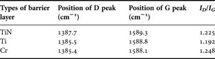
Characterization of the I D/I G parameter on the quality of the CNT growth was conducted using Raman spectroscopy as shown in Fig. 6. The Raman spectra have two peaks which usually fall in the range of 1370–1400 and 1580–1600 cm−1. The former peak is usually known as the D peak, which suggests the presence of defects; whereas the latter is known as the G peak, which indicates the presence of crystalline graphite. By analyzing the Raman spectrum, the type of CNTs present and their structural quality can be identified [Reference Yung, Wei, Wang and Tay23, Reference Dresselhausa, Dresselhausb, Saitoc and Jorio34]. Obtaining I D/I G as close to zero is usually desired, but CNT produced using PECVD have higher I D/I G due to the plasma-induced defects [Reference Sun35].

Fig. 6. Raman spectrum of the CNT grown on different barrier layers normalized to their G maximum intensity.
Table 1 shows that the CNTs on Ti present the lowest I D/I G data, which correspond to the aligned CNTs images shown in Fig. 5(b). Even though Sun et al. [Reference Sun35] reported that the quality of CNTs were independent of the Ni thickness and the underlying metal, we believe that the kind of underlying metal used could affect the quality of CNTs' growth. Current investigations also show that Ti and TiN were more suitable for the CNTs' barrier layer, because they formed silicide phases instead of carbide phases at high temperatures [Reference Nessim, Acquaviva, Seita, O'Brien and Thompson36]. The formation of carbides will deplete the carbon source available, hindering CNTs' growth. Therefore, the CNTs on Ti and TiN barrier layers appeared to be more graphitized and have less defects than the CNT grown on Cr. Based on the current study, we proposed to use either TiN or Ti for future barrier layers on Au to grow CNTs.
Table 1. Positions of D and G peaks, calculated I D/I G of Raman spectra of CNTs grown on different barrier layers.

IV. CONCLUSION
CNTs were successfully grown on gold line using PECVD process. Contrary to the DC analysis, the S-parameters of the Au coplanar lines did not show significant degradation after being subjected to high temperature and plasma. Cracks formed during the annealing of Au lines at 800°C were likely the cause of degradation as seen in the S-parameters measurements. After the plasma was introduced, the S-parameters were enhanced. This occurrence could have been caused by either plasma cleaning of the Au surface or increased surface energy which led to surface change on the Au film. This is an interesting observation and in-depth study into this phenomenon should be carried out. From the SEM micrographs and Raman analysis, the use of Ti or TiN as a barrier layer on Au is a better choice compared to Cr in terms of controlled CNT growth. However, detailed investigation on contact resistance between the CNT, barrier layer, and underlying metals is definitely necessary to optimize electrical performance in RF applications.
Thereafter, this study on the technological process will be applied to the design and fabrication of RF components and in particular for RF interconnecting applications.
 Yap Chin Chong received a degree in electrical electronics engineering (EEE) from the Nanyang Technological University of Singapore in 2009. After graduation, he began working on his Ph.D. degree at Nanyang Technological University. His major field of research is on the design and fabrication of CNT growth for interconnects applications.
 Tan Dunlin received her degree in electrical electronics engineering from the Nanyang Technological University of Singapore in 2005, and master degree in engineering (EEE) in 2009. She is now a research associate in the school of electrical and electronic engineering in Nanyang Technological University. Her research direction is in synthesis/characterization of carbon nanotube-based nanostructures and integration.
 Christophe Brun received his master degree from the University of Limoges in July 2010. He did his master degree internship at CINTRA UMI 3288 and he will start his Ph.D. on October 2010 in collaboration between XLIM and CINTRA labs. His research interests are focused on CNT modeling for RF packaging applications.
 Hong Li received a degree in electrical and electronic engineering from the Nanyang Technological University of Singapore in 2004 and received his Ph.D. degree in electronics engineering in 2008. His main research interests are electron transport in low-dimensional materials and systems.
 Teo Hang Tong Edwin received his Ph.D. in 2009 from the School of Electrical and Electronic Engineering in Nanyang Technological University (NTU), Singapore. He is currently working at NTU. His current interests include multiphase-carbon manipulation and nano-antenna design and implementation.
 Dominique Baillargeat received his Ph.D. degree in 1995 from the University of Limoges (France). He became full Professor in 2005. Since September 2009, he is the Director of CINTRA UMI 3288 and NTU Adjunct Professor. Before coming to Singapore, he was Professor at XLIM research institute in Limoges. He has authored more than 150 research articles and his current research interests include EM modeling and advanced CAD techniques dedicated to RF packaging and RF circuit design. He acts as expert for the French Research Agency (ANR). He acts as reviewer for IEEE MTT, IEEE MWCL and EuMW.
 Tay Beng Kang received his degree in engineering from the National University of Singapore in 1985, M.Sc. (electrical engineering) in 1989 and Ph.D. from the Nanyang Technological University of Singapore in 1999. He became a full university professor in 2006 and is currently the Associate Chair (Research) and the Program Director for the Nanoelectronics Materials & Devices Research Group in the School of EEE. He is one of the pioneer researchers in the filtered cathodic vacuum arc technology and is currently active in nano-engineering carbon-based hybrid systems.