


Introduction
Modern RF power amplifiers (PAs) applied in contemporary, high-throughput wireless system processing signals with a significant peak-to-average power ratio (PAPR) and wide bandwidth should meet contradictory requirements regarding linearity and efficiency. To maximize the output power level while keeping the high power-added efficiency (PAE), they typically operate as close as possible to the transistor peak power or use sophisticated methods as, e.g. the harmonic loading [Reference Raab1] or the Doherty architecture [Reference Doherty2]. Operation in non-linear regime with wideband and non-constant envelope waveforms usually entails the necessity to apply additional techniques to ensure compliance with linearity standard guidelines, expressed through in-band error vector magnitude (EVM) and out-of-band spectrum regrowth defined by adjacent channel leakage ratio (ACLR) or the shape of the spectrum mask. Although many techniques [Reference Cripps3] are considered for linearity and efficiency improvement together or separately, i.e. analog feedforward or feedback techniques, digital predistortion (DPD), dynamic biasing through envelope elimination and restoration [Reference Kahn4], envelope tracking [Reference Hassan, Kwak, Leung, Hsia, Yan, Kimball and Asbeck5], or Chireix's outphasing method [Reference Chireix6], only a few of them can be applied in the case of wideband spectrally efficient signals with high PAPR like WCDMA or LTE. The main reason for this limitation lies in the difficulties in analog hardware implementation of wideband RF signals phasing and summing, and fast envelope modulation used by the above-mentioned correction techniques. Moreover, typically as the output power of the PA increases, its bandwidth decreases. However, this issue is less noticeable in the case of GaN-based PAs. GaN technology allows designing PAs with wider bandwidth and extended compression region than, e.g. using GaAs MESFETs or Si LDMOSFETs. Moreover, in contrast to older technologies, GaN HEMTs (High Electron Mobility Transistors) make it possible to change bias in a wide range. Furthermore, thanks to DPD, the higher peak power can be obtained for GaN-based PAs.
The most commonly used technique for linearization of PAs in the currently designed broadband transmitters is the baseband DPD preceded by the shaping of waveform crest factor (CF) which is closely related to the architecture of contemporary wireless systems. In modern software-defined radio (SDR) transmitters, DPD methods [Reference Katz, Wood and Chokola7–Reference Wood9] are readily applied because of their relatively simple implementation in a digital baseband processor next to basic functionalities of transceivers. In such an architecture, the bandwidth of PA linearized by means of DPD depends only on D/A and A/D converters as well as digital signal processing capabilities, so it can be considered as a proper solution for more ultra-wideband standards in the future. Unfortunately, most of the known power efficiency improvement methods based on RF hardware remain frequency restricted.
The vast majority of publications related to PA linearity or DC efficiency improvements focus on the description of the methods themselves. PAs used to test these methods are treated as a black box with a predefined DC operating condition. This paper contains the results of a case study concerning RF PAs on the interactions between DC operating conditions, linearizability, power efficiency as well as effectiveness of DPD processing. Furthermore, the impact of transistor bias conditions on the shaping of linearity and power efficiency of amplifiers is also considered. For this purpose, optimization of the transistor operating point is the way to meet the extreme requirements on the modern wireless standards such as LTE. The subject of our study is focused on GaN HEMT class A, AB, and almost B RF PAs, especially. To the best of the authors’ knowledge, there is no publication in this field. The important issue from the perspective of PAs’ designers is also to check the applicability of the well-known small-signal approach to design the RF amplifiers excited by wideband and high PAPR signals. It seems that the drawbacks of small-signal modeling can be partially reduced or taken into account using transistor bias optimization together with DPD processing.
Below we present the results of studies on the effect of GaN HEMT biasing conditions on PA linearity and the effectiveness of DPD, which were performed using 10 and 150 W PAs and LTE20 standard test signal. We focused on the conventional DPD technique with the indirect learning architecture (ILA) employing the memory polynomial (MP) model of PA non-linearity.
PA design method, PA, and HPA description
GaN technology
Due to the high thermal and voltage robustness as well as high-power density, GaN HEMTs are the excellent choice to design high-power and high-efficiency microwave amplifiers for various applications such as wireless communications, radars, and microwave heating. Typically, the drain-to-source breakdown voltage exceeds 100 V and allowable gate-to-source voltage (U GS) range is from −10 to 2 V. GaN HEMTs are normally recommended to operate in class AB at a typical quiescent operating point with DC drain-to-source voltage U DS = 28 or 50 V (low or high voltage GaN HEMTs, respectively) and small quiescent drain current I DQ (U GS is slightly above the gate-to-source threshold voltage).
For comparison, the RF power depletion- or enhancement-mode GaAs FETs should be operated in class A or “little depth” AB (quasi A-class) with DC drain-to-source voltage U DS = 10/12 V and the high quiescent drain current I DQ, close to a half of the saturated drain current. The absolute maximum ratings of GaAs FETs are as follows: the breakdown voltages of drain–source U BR = 15 V, gate–source U GS = −5 V, and the maximum channel temperature of 175 °C. GaN HEMT may be operated correctly with a channel temperature above 250 °C. Due to the biasing conditions combined with high-voltage robustness of GaN HEMT, the high efficiency of PAs is obtained. Moreover, the efficiency may be even more increased using the fact that the output capacitance of the transistor is almost independent on the drain-to-source voltage in the wide range of this voltage. Hence PAE of GaN HEMT amplifier is higher ca. of 20 percentage points than a typical PAE value for GaAs FET PA.
The higher U DS voltage at low saturated drain current I Dsat of GaN HEMTs allows achieving the maximum output power at the higher load resistance value than in case of GaAs FETs. It makes the output matching network and biasing circuit easier to design and the amplifiers’ bandwidth can be wider.
PA design method
One of the assumed research goals was to check the DPD linearization capability for PAs designed using the small-signal approach without non-linear modeling of the transistor. The non-linear modeling requires either very intensive measurements and numerical calculations or accurate models. In many cases of engineering practice, it is not necessary to use such an advanced apparatus to design class A or AB PAs, which dominate in wireless communications. As above mentioned, in the design of PAs, the small-signal approach was used. An example of this approach is the very popular Cripps method [Reference Cripps10]. The load impedance optimal for the maximum output power level based on DC I–V characteristics and small-signal output impedance at a given transistor operating point is determined in this method. The impedance condition proposed by Cripps suggests a series circuit as the load, leaving aside the actual structure of the transistor output circuit, which in the HEMT case has a parallel circuit structure – parallel connection of C ds and R ds as shown in Fig. 1. Therefore, the definition of the admittance condition in the plane of controlled current source seems natural [Reference Walker11]. Determination of the admittance condition within the transistor helps to incorporate wire connections and other parasitic elements as well as internal matching sections based on clamps measurements. To take advantage of the admittance condition, a small-signal transistor model is needed. For that purpose, a methodology of the extraction of elements of the equivalent circuit was developed based on the measurement of S-matrix only for three operating points, i.e. for the states: turned off (U GS ≤ U Thershold, U DS = 0 V or U GS ≤ U Thershold, U DS = U DSQ), turned on (U GS = 0 V, U DS = 0 V), and in the planned work conditions (U DS, I D = I DPM) [Reference Wojtasiak and Gryglewski12,Reference Wojtasiak, Gryglewski and Sędek13]. The drain current I DPM corresponds to the peak or at least average output power and results from the performances of transistor and signal standard (PAPR). The concept of the proposed method is shown in Fig. 1. A resistance R opt is an optimum resistance for the assumed output power level and can be determined from DC I–V characteristics of the transistor. The modeling procedure can be implemented in one of the microwave circuit simulators, e.g. in the ADS.

Fig. 1. The proposed small-signal approach for designing of HEMT/MESFET power amplifiers.
The values of model parameters are calculated in the process of fitting the measured and simulated S-matrix elements of a transistor in the significantly wider frequency range than the desired amplifier band. A lower frequency of the fitting range should be up to several hundred MHz. While the upper frequency has to significantly exceed the upper end of the amplifier band. Introduction of excess amount of data in the form of three S-matrices for the three operating states of transistor leads to the better conditioning of numerical problem and acceleration of calculations. Subsequently, the synthesis of matching networks and biasing circuits is performed for the maximum output power within a given frequency range under the condition of system stability for given values of gain and reflection at the amplifier input. The amplifier should be stable for each frequency, and not only in its working band. The input matching network of PA is directly designed using the measured S-matrix of the planned bias of transistor. Due to a limited transistor isolation (S 12 ≠ 0), the admittance condition and other requirements can be met by an iterative process. Because of adding the matching network to the transistor's input, the output admittance changes in the selected plane. The output matching network should be corrected to include this change in the load admittance and again meet the admittance condition. Correction of the circuit output forces the tuning of the network at the transistor input to achieve the assumed gain and return loss in the required band. In subsequent iterations, the procedure is repeated until satisfactory results are obtained.
DUT description
As mentioned before, two different amplifiers 10 W PA and 150 W HPA were used during the experiments. A single-ended ISM 2.45 GHz-band amplifier (PA) with a general purpose CGH27015F GaN HEMT from Wolfspeed [14] was designed based on the non-linear model provided by Wolfspeed. The PA achieves more than 20 dB small-signal gain and 40.5 dBm output power level at the 1 dB gain compression point for the bias of 28 V drain-to-source voltage and 0.5 A quiescent drain current. An additional heatsink with air cooling was used to improve the thermal conditions.
Due to the poor technical data (the lack of transistor model, S-parameters or values of source and load impedances) required for design the HPA, NXP A2G35S200-01S GaN HEMT [15] was chosen here to show the process of amplifier designing by means of the proposed small-signal approach. Therefore, this transistor was chosen here, as an example, to show the process of amplifier designing by means of the proposed small-signal approach. The extracted A2G35S200-01S model at the operating point U DS = 48 V and I D = 2 A is shown in Fig. 2. U DS = 48 V is recommended by NXP and I D = 2A resulted from the thermal limitations for CW operation.

Fig. 2. A2G35S200-01S GaN HEMT small-signal model at U DS = 48 V, I D=2 A, and S-parameters over 0.6–4.2 GHz frequency range, red – measurements, blue – simulations.
As shown in Fig. 2, A2G35S200-01S GaN HEMT includes internal matching sections optimized from 3.4 to 3.6 GHz frequency range. According to our method, the load admittance Y L for the output power of 200 W was determined for the center frequency of 3.5 GHz and is equal to 0.15 + j0.14 S. The developed HPA achieves the output power level more than 150 W over a 3.4–3.6 GHz frequency range. The comparison of measured and simulated small-signal characteristics of HPA, i.e. input return loss and gain versus frequency is shown in Fig. 3.

Fig. 3. Input return loss and gain of HPA versus frequency.
The manufacturer (NXP) declares 225 W peak output power, but at the 3 dB gain compression point calculated as P 3dB = P AVG + 7 dB, where P AVG = 40 W average output power measured using an unclipped WCDMA single-carrier input signal and output PAPR is compressed to 7.0 dB at CCDF of 0.01%. These data are given for one frequency from 3.4 to 3.6 GHz band at the quiescent operating point U DS = 48 V, I DQ = 0.3 A. For improvement of thermal conditions, water cooling was used.
To sum up, the parameters of both amplifiers are collected in Table 1 and their photos are presented in Fig. 4. The DUTs’ measurements were performed with CW pulsed signal (10% duty) for DC operating condition suggested by the transistors’ manufacturers.
Table 1. Parameters of PA and HPA under test

a Efficiency in 1 dB compression for pulsed CW (10%) excitation.

Fig. 4. Photos of: (a) PA and (b) HPA.
The transfer P OUT(P IN) characteristics measured for a few frequencies are also presented in Fig. 5 as a supplement to Table 1.

Fig. 5. P OUT (P IN) characteristics of: (a) PA (U DS = 28 V, I D = 0.5 A), (b) HPA (U DS = 48 V, I DQ = 0.3 A).
Digital predistortion technique
Nowadays the baseband DPD technique seems to be one of the most widely employed methods for linearization of RF PAs [Reference Katz, Wood and Chokola7], primarily because of its relative simplicity and cost effectiveness, especially when it is implemented in SDR-based transmitters. The basic principle of DPD consists of the non-linear transformation of the input complex baseband I/Q signal in order to pre-compensate distortions caused by the inherent non-linearity of PA. This operation is realized digitally in a functional block called a predistorter whose transfer function should be as close as possible to the inverse of the non-linear PA transfer function.
Since the PA non-linearity can vary with time due to changes of PA operation conditions, the transfer function of the predistorter should be continuously updated to keep the linear operation of PA with DPD, which entails the application of adaptive predistorters [Reference Ghannouchi, Oualid and Helaoui8].
Our goal was to study how the choice of PA DC operating conditions affects linearizability, efficiency, and effectiveness of DPD. For this purpose, we decided to use the quite conventional, widely used predistorter with the ILA [Reference Eun and Powers16] and the MP model of PA non-linearity [Reference Ding, Zhou, Morgan, Ma, Kenney, Kim and Giardina17,Reference Kim and Konstantinou18].
The ILA predistorter structure considered in this paper is shown in Fig. 6 [Reference Ding, Zhou, Morgan, Ma, Kenney, Kim and Giardina17]. The predistorter with the input x(n) and the output z(n) is a copy of the training predistorter (A) which estimates the inverse model of PA, taking as an input the PA output signal y(n) divided by the average gain G of PA, and as an output the PA input signal z(n) which is equal to x(n) in the first step of DPD processing. All signals x(n), z(n), y(n) appearing in this scheme are considered as complex baseband signals. The predistorter coefficients estimated by means of the training predistorter are used to pre-compensate the input signal x(n). To make possible to compensate the higher order intermodulation products introduced by the PA non-linearity, the bandwidth of the predistorted signal z(n) needs to be wider in comparison to the input baseband I/Q signal. Therefore, the input signal is oversampled before the input of the predistorter. The oversampling rate 5 is commonly used to capture the products of 3rd and 5th order. Moreover, the output signal y(n) is sampled with the same frequency and other analog components of the system should ensure the required bandwidth suitable for predistortion processing.

Fig. 6. Indirect learning architecture of DPD.
Before calculations of the predistorter coefficients, the measured samples y(n) at the PA output need to be aligned in time to the input samples z(n), which is usually done in two stages. Firstly, a coarse alignment is performed using cross-correlation, which enables us to align the signals to the nearest sample. Then, a fine so-called subsample alignment is performed by phase alignment using the average angle between output and input samples, estimated from a given set of input and output samples.
Apart from the predistorter architecture, another crucial issue in DPD is a model of PA non-linearity. There are many non-linearity models used for PA description, see e.g. [Reference Ghannouchi, Oualid and Helaoui8, Reference Wood9]. The most frequently used models originate from Volterra series [Reference Schetzen19] which can be considered as a non-linear extension of finite impulse response linear filters. Among these models, the very widespread model used in DPD systems is an MP model [Reference Katz, Wood and Chokola7, Reference Ghannouchi, Oualid and Helaoui8] which can be successfully used for modeling the memory effects occurring in PAs. Because of the computational effectiveness and quite convenient and efficient way of implementation, the MP model is very popular and widely used. The MP model of PA non-linearity is described by the following formula:
 $$y(n) = \sum\limits_{k = 1}^K {\sum\limits_{m = 0}^M {b_{k,m}z(n-m){\vert {z(n-m)} \vert } ^{(k-1)}}}, $$
where K is the order of the polynomial, M is the memory depth, and b k,m are the coefficients of the MP model. In the ILA predistorter, the coefficients of the inverse model of PA can be expressed as follows:
 $$\eqalign{z(n) & = \sum\limits_{k = 1}^K {\sum\limits_{m = 0}^M {a_{k,m}u(n-m){\vert {u(n-m)} \vert } ^{(k-1)}}} \cr & = \sum\limits_{k = 1}^K {\sum\limits_{m = 0}^M {a_{k,m}u_{k,m}(n)}}}, $$
where u(n − m) = y(n − m)/G, u k,m(n) = u(n − m)|u(n − m)|(k−1) and a k,m are the coefficients of the inverse PA model. To estimate the coefficients a k,m, the standard linear squares (LS) method is commonly used:
 $${\hat{\bi a}} = ({\bi U}^H{\bi U})^{-1}{\bi U}^H{\bi z},$$
where  ${\hat{\bi a}} = [\hat{a}_{1,0},...,\hat{a}_{K,0},...,\hat{a}_{1,M},...,\hat{a}_{K,M}]^T$ is the vector of the coefficients’ estimates,
  ${\bi U} = [{\bi u}_{1,0}, \ldots, {\bi u}_{K,0}, \ldots, {\bi u}_{1,M}, \ldots, {\bi u}_{K,M}]$ is the regression matrix and the vectors
  ${\bi u}_{k,m} = [u_{k,m}(0), \ldots, u_{k,m}(N-1)]^T$ are calculated on the basis of N samples u(0), …, u(N − 1) of u(n) signal, and
  ${\bi z} = [z(0), \ldots, z(N-1)]^T$ is the vector of N samples of PA input z(n).
The model coefficients were determined using the LS method as in (3) over the collected sets of data assuming in the first training phase that z(n) = x(n), i.e.  ${\bi z} = {\bi x} = [x(0),...,x(N-1)]^T$. Finally, the pre-distorted signal given at the input of PA is calculated as follows:
 $$z(n) = \sum\limits_{k = 1}^K {\sum\limits_{m = 0}^M {{\hat{a}}_{k,m}x(n-m){\vert {x(n-m)} \vert } ^{(k-1)}}}. $$
After many series of tests performed with the considered PAs, we decided to set the parameters of the MP model of PA as K = 5 and M = 1. The number of samples used to calculate the model coefficients was set to N = 104.
Experiments
The aim of the experiments was to evaluate the impact of DC operating point of the transistor on PA linearity factor expressed by ACLR and EVM as well as on DC supply efficiency. It is assumed that the reduction of U DS and I D will allow the improvement of the power efficiency at the expense of linearity degradation and P1 dB compression points move down. Additionally, the DPD procedure should compensate the last two effects and lead to a compromise between the power efficiency and linearity. To achieve the output power level as high as possible, the relative changes of U DS and I D were limited to several percentages.
To generalize the conclusions from our measurements, two significantly different single-ended amplifiers with GaN HEMTs were considered, i.e. 10 W ISM 2.45-band PA and 150 W 3.5 GHz Telecom-band HPA.
The transistor biasing conditions were selected to use the allowed range of current and voltage changes resulting from DC I–V characteristics of GaN HEMT without exceeding the maximum power dissipation and with account the manufacturers’ recommendations. At almost all considered operating points, the input power level was set to obtain the peak output power level higher than 10 W for PA and 150 W for HPA at CCDF = 0.01%. It is worth noting, that no CF reduction processing was used. Thus, after applying it, further efficiency improvement of a few percent could be expected. The measurements of amplifiers excited by 2.45 GHz (PA) and 3.5 GHz (HPA) signals modulated by one looped frame of E-TM1.1 test model waveform [20] were performed.
Measurement setups
The measurement setups used in experiments is presented in Fig. 7. ADRV9371-W/PCBZ evaluation FMC card [21] within Xilinx ZC706 motherboard delivers (TX port) E-TM1.1 signal dedicated for LTE20 spectrum emission testing, specified in TS36.141 [20]. The same evaluation FMC card is simultaneously used as a DPD observation receiver (ORX) to monitoring non-linearities at the output of DUT. The AD9371 card is SDR-based transceiver with integrated baseband DSP unit, ADCs, DACs, and analog direct up- and down-conversion stages allowing transmitting and receiving RF signals up to 100 MHz bandwidth in 300 MHz to 6 GHz frequency range. The device during experiments runs with 122.88 MS/s IQ sampling rate both for transmitter and receiver signal paths. It means four times oversampling and gives more than five times wider band of spectrum observation. IQ signal generation for the transmitter with DPD processing and measurement procedures is developed in Matlab and Python. During experiments, the DPD procedure described in section “Digital predistortion technique” was performed. N9020 spectrum analyzer with RBW = 910 kHz and VBW = 300 Hz for traces smoothing was used for spectra measurements.

Fig. 7. Measurement setups used to test the PA (a) and the HPA (b).
The amplifiers under test were driven by drivers with two configurations. For PA test, two M/A-COM MAAM26100 amplifiers were applied as the drivers. In the case of HPA, the third stage with Wolfspeed's CGH40010 transistor was added. The special effort was carried out to keep the non-linearity at the input of the tested amplifiers on the negligible level. The spectra of testing signals for both setups are presented in Fig. 8. As shown in Fig. 8(b), the third driver introduces some spectral regrowth to the signal at the HPA input. This non-linearity is finally reduced together with the non-linearity of HPA by means of the DPD procedure.

Fig. 8. Normalized spectrum at the inputs of the PAs under test: (a) 10 W PA, (b) 150 W HPA.
The signal from the output of the measured amplifier is attenuated and then delivered to the N9020 spectrum analyzer used here for the measurement of ACLR, EVM, average power level, and CCDF. It also is directed to the input of the ORX in the AD9371 card for DPD purposes. As recommended in TS36.141, the compliance level of ACLR at the output of the tested amplifier needs to be <−45 dBc.
Results of experiments: PA linearity versus efficiency without DPD
At the beginning of the experiments, ACLR, rms EVM, corresponding drain efficiency η D, and PAE at the chosen bias points of both amplifiers without DPD correction were calculated. The results of the 10 W PA are shown in Table 2. The spectrum regrowth is strongly dependent on the transistor drain–source voltage U DS than the drain current I D changes when the relative values are analyzed. It means that I D can be reduced more and thus the DC efficiency can be improved. The average drain currents are close to operating points, which confirms the operation in class A or AB (close to A).
Table 2. Peak power level, ACLR, and power efficiency factors for the 10 W PA without DPD for chosen operating points

As indicated by bolded parameters (compromise operating condition) in Table 2, the similar level of non-linearity products at the output of PA for significantly different DC power consumption can be obtained and PAPR levels are decreased, as expected, at the transition from class A to deeper AB class. PA operation for the bias U DS = 24 V and I DQ = 0.5 A seems to be a good trade-off for such parameters as ACLR, PAE, and peak power level of the tested PA.
The results obtained for HPA at the drain currents I DQ ranging from 0.6 to 0.1 A (and additionally for 1.8 A) are presented in Table 3. As shown in Table 3 the differences in linearity and especially power efficiency are less significant compared to PA results. As it can be observed in the table, regardless of the assumed quiescent drain current I DQ (RF-off), the changes of average drain currents are small. This fact is typical for the amplifier operation close to class B. It also means that in the case of HPA, the load impedance value and average drain current (RF-on) affect the linearity end efficiency more than the RF-off drain current I DQ.
Table 3. Peak power level, ACLR, and efficiency factors of the 150 W HPA for chosen operating points, without DPD correction

Additional tests with very high I DQ of 1.8 A, close to A class operating point and significantly different than biasing current (0.3 A) recommended by NXP, show that the linearity, peak power level as well as efficiency factors have even worsened. It can be most likely associated with limited heat dissipation resulting in a rise of temperature inside the transistor. Consequently, the load impedance becomes suboptimal.
After the first stage of experiments, operating point U DS = 45 V and I DQ = 0.3 A was chosen as the nearly optimal bias condition taking into consideration the need for simultaneous maximization of the output power level, linearity, and power efficiency. This bias point is also suggested by the manufacturer of the transistor. Probably the internal transistor structure was optimized for this operating point.
Summarizing the PA and HPA measurements without DPD, it should be noted that none of the amplifiers in any of the tested operating point for the output power close to and above 1 dB compression point meets the requirements for LTE system linearity defined by ACLR level as less as −45 dBc.
Results of experiments: after DPD
The second part of experiments concerned an improvement of PA linearity and power effectiveness by means of application of DPD procedure described in section “Digital predistortion technique”. For both amplifiers, the best results were obtained for the MP model of PA non-linearity with the following parameters K = 5 and M = 1 (see section “Digital predistortion technique”) which were determined by means of multiple tests and evaluation of spectral regrowth improvement as well as AM/AM and AM/PM characteristics [Reference Ghannouchi, Oualid and Helaoui8]. During the tests, only the operating points for which the ACLR is better than −45 dBc and the output peak power exceeds 10 W (PA) and 150 W (HPA) were considered.
The output spectra of the 10 W PA without and with DPD for various currents I D and voltages U DS equal to 28 and 24 V are shown in Figs 9(a) and 9(b), respectively. The spectral regrowths after DPD are in this case similar in shape but shifted proportionally to distortions.

Fig. 9. Spectra of the 10 W PA before and after DPD correction.
The results of the improvement of PA parameters after applying the DPD procedure are summarized in Table 4. Typical improvement of ACLR is in the range from 14.7 to 18.5 dB at PAPR higher than 8 dB or even 9 dB. The measurements with the lowest U DS voltage are the exception where DPD correction is very poor. For one operating point (U DS = 20 V, I DQ = 0.3 A) even deterioration is noticed when the PA is operated in hard compression and DPD method does not then work correctly. The in-band linearity factor, i.e. EVM is for all operating points with U DS = 28 or 24 V lower than 2% except for the point with U DS = 28 V, I DQ = 0.5 A, when EVM is slightly larger. It is worth noticing that PAPR and EVM obtained after DPD does not change monotonically with changes in operating conditions for tested PA. For I DQ = 0.5 A, a slight deterioration of these parameters is noticed. The improvement of PAE between the highest and lowest biasing current with acceptable ACLR of −47.5 dBc changes from 6.8 to 16.1% which is more than two times.
Table 4. Linearity and power efficiency factor measurements of the 10 W PA before and after DPD correction

Finally, the operating point of 24 V and 0.3 A is chosen because of the satisfactory linearity of ACLR = −47.5 dBc, EVM = 1.4%, PAE = 16.1%, and the output peak power level of 40.5 dBm at 9.7 dB of PAPR.
The similar experiments as for PA were performed for HPA. In Fig. 10, the 150 W HPA spectra are presented for both 50 and 45 V U DS bias voltages and chosen I DQ currents. As shown in Fig. 10 the lack of symmetry of the spectra after DPD is noticeable. It was initially assumed that the reason was the lack of sufficient shielding of amplifiers. Despite the device was successfully shielded and the use of circulator to minimize the high load impact, the asymmetry remained. Likely, this effect results from the asymmetry of the gain characteristic around 3.5 GHz.

Fig. 10. Spectra of the 150 W HPA before and after DPD correction.
The quantitative results obtained for HPA are presented in Table 5. As in the case of experiments without DPD, the efficiency factor PAE changes slightly from about 21.4% for U DS = 50 V and I DQ=0.6 A to over 25.6% for U DS = 40 V and I DQ = 0.1 A, except the measurement for I D = 1.8 A. The ACLR improvement factor is between 18.1 and 10.7 dB at PAPR level higher than 9 dB, and decreases with the biasing current. The EVM level is lower than 2.3% for all considered biasing points.
Table 5. Linearity factor measurements of 150 W HPA before and after DPD correction

According to the data from Table 5 the most optimal operating point (U DS = 45 V, I DQ = 0.3 A) there is close to manufacturer recommendation. For this operating condition, the following parameters have been obtained after DPD: ACLR = −51 dBc, EVM = 1.7%, PAE = 23.4%, and the output peak power level of 51.9 dBm at 9.1 dB of PAPR at CCDF = 0.01%.
Results of experiments: DPD procedure tests
Separate tests regarding the effectiveness of DPD procedure were also performed. It was confirmed that linearization does not change the average output power but only increases the peak power and PAPR through expanding the linearity region by at least 1 dB as illustrated by the characteristics of normalized gain in Fig. 11.
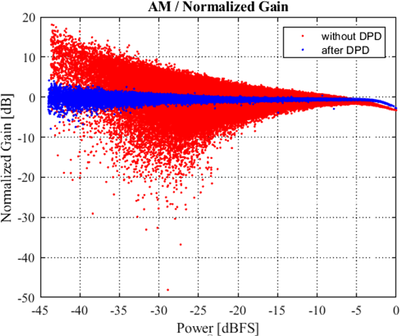
Fig. 11. Normalized gain of HPA.
As shown in Fig. 12 the memory depth parameter M is changed from 0 to 3, the best modeling of the memory effect was obtained for the only one delay sample taking into consideration during DPD procedure.

Fig. 12. The effect of DPD procedure memory depth parameter on HPA spectrum: (a) M = 0, (b) M = 1, (c) M = 2, (d) M = 3.
Due to the use of a one-iteration DPD based on LS method as described in section “Digital predistortion technique”, the impact of self-heating of the transistor was also tested. The spectra measured after 5 and 10 min after the execution of the DPD procedure under the established thermal conditions are shown in Fig. 13.

Fig. 13. HPA spectra after specified time from DPD procedure execution.
As shown in Fig. 13, very slight differences in spectra are noticed, which suggests maintaining a very stable temperature in HPA transistor structure due to the high thermal time constant describing thermal behavior of GaN HEMT as well as the use of water cooling. Maintaining stable thermal conditions enables the impact of PA transistor self-heating phenomena on test correctness to be significantly reduced. Therefore, the compensation procedure can be repeated every few tens of minutes.
Assessment of the effectiveness of the implemented DPD procedure was the subject of the last series of experiments. DPD method used in the experiments was only the tool to evaluate the DC operating condition on DPD linearizability and power efficiency of PAs, so the limitations of the method in hard compression region have been already known at the beginning of the experiments. On the other hand, the results reported in other publications which can be comparable to our results are very limited because of the different experiment scenarios, e.g. different input waveforms, power levels, transistors used in PAs, amplifier structures, thermal conditions (cooling). Therefore, to confirm the credibility of our DPD implementation, the dedicated system AD9375 [21] with the embedded modern DPD solution delivered by the manufacturer was used as a reference. The results obtained using our measurement setup with DPD (section “Digital predistortion technique”) and by means of AD9375 [21] were compared under the same conditions and exemplary spectra are shown in Fig. 14. After these experiments, we can conclude that our DPD implementation gives slightly worse results but still satisfactory for the planed applications.

Fig. 14. Comparison of DPD implementations: U DS = 28 V, I D=0.5 A (left), U DS = 24 V, I D=0.3 A (right).
Conclusions
The results of the studies presented in the paper show that the combination of DPD and optimization of DC operating condition of a PA transistor can allow the optimization of DC power consumption with simultaneous ACLR and EVM level control in wideband RF systems. It is worth noting that for the 10 W PA general purpose transistors operating in class A or AB, the achieved compromise was more spectacular than for 150 W HPA.
Although HPA transistor is operated substantially at well-defined operating conditions in the deep class AB and its structure is by factory optimized for both maximal output power level and linearity the further optimization can be achieved only by tuning of the output load. On the basis of the determined optimum load impedance values versus frequency at the new operating point, the output matching network can be designed. This task is difficult in itself. In addition, the experiments show, that regardless of the output power level of PA or HPA, the compromise between linearity and power efficiency can be achieved only with DPD and the average drain current should be close to one-quarter of the maximal allowed drain current.
The paper presents also the results of studies on the development and practical verification of the proposed PA design method using the small-signal approach. The HPA designed on the basis of the small-signal transistor models required only fine re-tuning. The HPA parameters confirm that the small signal approach to transistor modeling supported by the proper choice of DC operating condition and DPD linearization enable the PAs for modern wideband systems to be designed. It is worth noticing that the PA and HPA were tested to determine their linearity and energy efficiency using as excitation the CW, CW pulsed, and LTE 20 MHz signals.
Summarizing our studies, we can conclude that the development of high-performance PAs for the modern wireless systems with significant PAPR and wide bandwidths require the combination of advantages of GaN HEMT technology with DPD techniques and optimization of PA transistor bias condition for both PA linearization and PA power efficiency improvement.
Author ORCIDs
Konrad Jędrzejewski, 0000-0003-4303-9450; Dawid W. Rosolowski, 0000-0001-6892-7820; Wojciech Wojtasiak, 0000-0002-6422-7154.
Acknowledgement
Power amplifiers used for the measurements were completed as part of the UE project POIR.01.01.01-00-0610/16.
 Konrad Jędrzejewski received his M.Sc. degree in electronics and telecommunications and the Ph.D. degree in electronics, in 1995 and 2000, respectively, from the Faculty of Electronics and Information Technology, Warsaw University of Technology (both with honours). He received the D.Sc. degree in electronics in 2014. Since 2000, he is a Professor in the Institute of Electronic Systems, Warsaw University of Technology. His main research interests include statistical and adaptive signal processing, A/D converters, especially converters employing adaptive algorithms for A/D conversion, adaptive measurement and telecommunications systems, and radar signal processing.
 Dawid W. Rosolowski received his M.Sc. and Ph.D. degrees in electronics in 2005 and 2011, respectively, from the Faculty of Electronics and Information Technology, Warsaw University of Technology. Since 2012, he is an Assistant Professor in the Institute of Radioelectronics and Multimedia Technology, Warsaw University of Technology. His current research interests include microwave technique, SDR technology, reconfigurable front-end and wireless system designating in particular adaptive power amplifiers and digital signal processing of wireless signal with FPGA.
 Wojciech Wojtasiak received the M.Sc., Ph.D., and D.Sc. degrees in electronic engineering from the Warsaw University of Technology, Warsaw, Poland, in 1984, 1998, 2015, respectively. He is currently a Professor at WUT and the Head of Microwave and Radiolocation Engineering Division. Since 1990 his research activity concentrates on the design of high-frequency-stability microwave high-power solid-state sources and transmitters. Now, he has been also engaged in the research on GaN HEMT technology and thermal analysis in the time domain of high-power microwave FETs. Since 1998 he has been a member of IEEE.


