


I. INTRODUCTION
The data rates in digital communication are on the rise and are currently in the range of several tens of Gbit/s for wired systems, whereas current wireless networks achieve data rates of several 100 Mbit/s. Breaking the wireless Gbit/s barrier is necessary to overcome a bottleneck in wireless communication to serve the next generation of wireless personal area networks and wireless video distribution.
Applications such as high definition video streaming or telemedicine require high transmission rates, and besides higher spectral efficiency the available channel bandwidth is a key factor in achieving ultra-high data rates over the air. The future of wireless data transmission will therefore be around 60 GHz where up to 7 GHz of channel bandwidth are available in the EU, USA, Canada, and Korea in the recently allocated frequency range from 57 to 64 GHz. With increasing operating frequency, attenuation and scattering grows which leads to a lower signal-to-noise ratio that can be faced by increasing the transmitter power or improving the receiver sensitivity. The high electron mobility transistor (HEMT) concept features higher power density and lower noise figure compared to high-frequency CMOS or SiGe technologies and is able to fulfill the demanding requirements in high-performance 60 GHz communication scenarios, such as medium range (up to 10 m) applications or channel sounding. Table 1 shows a comparison of essential 60 GHz building blocks in different semiconductor technologies. For our in-house HEMT technology, we use standard GaAs substrates to manufacture a metamorphic high electron mobility transistor (mHEMT) with an InGaAs channel providing InP-like performance.
Table 1. Comparison of reported 60 GHz building blocks in different MMIC technologies.

In this paper, we present the design and performance of mHEMT-based 60 GHz analog transceiver components, which are intended as high-performance frontends for combination with subsequent SiGe- or CMOS-based transceiver components:
– A single-chip 60 GHz transmit and receive amplifier with antenna switch and differential radio frequency (RF) interface can boost the transmit power and receiver sensitivity of an Si-based frontend.
– A single-chip transceiver with antenna switch and subharmonically driven IQ down- and up-converter stages is designed for the hybrid combination with a high-quality 30 GHz Voltage Controlled Oscillator (VCO) in e.g. SiGe Heterojunction Bipolar Transistor (HBT) technology. The chip features an antenna switch and a single I/Q mixer for down- and up-conversion.
II. TECHNOLOGY
The mHEMT technology of the Fraunhofer IAF features currently three different gate lengths from 100 nm down to 35 nm for MMICs working up to 450 GHz. The transistors are grown on 4″ GaAs substrates via molecular beam epitaxy. A metamorphic buffer layer is used to adapt the lattice constant between the substrate and the main channel. During the growth of the metamorphic buffer, a linear InxAl0.48Ga0.52−xAs (x =0 → 0.52) transition is used. For the 100 nm gate length technology, the electrons are confined in an In0.65Ga0.35As/In0.53Ga0.47As composite channel to increase the breakdown voltage. The electrical characteristics of the different mHEMT technologies are summerized in Table 2. Further information about the Fraunhofer IAF mHEMT technology can be found in [Reference Leuther6, Reference Tessmann, Kallfass, Leuther, Massler, Schlechtweg and Ambacher7] (Table 2).
Table 2. Electrical characteristics of the Fraunhofer IAF mHEMT technology.
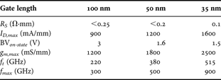
For 60 GHz applications, the 100 nm variant is best suited, offering comfortable cutoff frequencies f T and f max of 220 and 300 GHz, respectively, in combination with a relatively high on-state breakdown voltage of 3 V.
III. 60 GHz LOW-NOISE AMPLIFIER (LNA)
The LNA is the most critical element of the receiver frontend. It amplifies the received signal and mainly determines the overall noise figure of the receiver. Since transmit power is typically limited by the regulation authorities, the receiver sensitivity becomes more important to improve the link budget and increasing the link availability. Hence, the two major design goals are gain and low noise. The realized 60 GHz LNA achieves more than 20 dB small-signal gain combined with a noise figure of <2.5 dB in the frequency range of interest from 55 to 65 GHz. Reported SiGe LNAs for 60 GHz applications achieve gain values of 20 dB with a noise figure of 6 dB [Reference Yaoming, Herzel, Borngraber and Kraemer8, Reference Van-Hoang, Subramanian and Boeck9] down to 4.5 dB with 15 dB gain [Reference Floyd, Reynolds, Pfeiffer, Zwick, Beukema and Gaucher1].
The design uses a three-stage common-source topology with a transistor size of 4 × 15 µm. The measured 3 dB bandwidth equals 30 GHz from 45 to 75 GHz and covers the entire V-band (50–75 GHz). The input and output return loss stays well above 10 dB from 49 to 74 GHz. Noise matching is achieved via the inductive source degeneration technique, implemented by symmetrical shorted stubs inserted in the source terminals of the transistors. The measured S-parameters of the LNA are shown in Fig. 1.

Fig. 1. Measured S-parameters of the 60 GHz LNA.
The chip photograph of the receive/transmit amplifier in Fig. 4 contains the LNA stage in the receive path.
IV. MEDIUM POWER AMPLIFIER (MPA)
The MPA is driving the antenna and should provide gain as well as output power. The MPA was designed to operate in the frequency range from 55 to 65 GHz. The desired maximum output power was 100 mW (20 dBm) in this frequency range. Although higher transmit power would be useful regarding the link budget, it is limited to 10 dBm in many countries in the 60 GHz band by the regulation authorities. These limitations allow the operation of the MPA with more than 4 dB back off, which guarantees sufficient linear operation.
The design uses two parallel 6 × 60 µm dual-gate stages. As a stand-alone circuit, the MPA consists of two cascaded stages. The first stage uses a single 6 × 60 µm cascode to provide an additional amplification of approximately 11 dB. The second stage with two parallel transistors adds a small-signal gain of approximately 9 dB to achieve a total small-signal gain of 20 dB.
The chip photograph of the receive/transmit amplifier in Fig. 4 contains the second MPA stage only in the transmit path.
The cascode amplifier is biased under class-A conditions at a drain supply voltage of 3 V and a drain current density of 305 mA/mm. The amplifier consumes a total DC power of 1 W.
The measured performance is shown in Fig. 2. Small-signal gain is 20 dB in the frequency range from 56 to 65 GHz. The one-tone power measurement at 60 GHz shows a saturated output power of 20 dBm and an output-related 1-dB compression point of 14.4 dBm. The power-added efficiency is 8%. The amplifier shows a very broadband behavior also in terms of its output power, which stays nearly constant at 20 dBm in the frequency range from 55 to 65 GHz.

Fig. 2. Small-signal gain, matching and saturated output power of the medium power amplifier over the RF frequency (a) and the output power, gain, and power-added efficiency versus the input power (b).
V. ANTENNA SWITCH
Altering between receive and transmit operation requires on-chip integrated switches. The mHEMT technology allows the design of low loss, high isolation switches. The realized 60 GHz single-pole double-throw (SPDT) switches use two transistors in each branch with a 2 × 40 µm configuration. The switching transistors are inserted in shunt across the signal line, with their channel acting as voltage-controlled resistor, which can short circuit the signal when the transistor is biased above threshold. A series quarter-lambda line transforms the short circuit to an open circuit in order to achieve branch isolation. A shorted stub placed between the two shunt transistors is acting as a parallel inductance and achieves a parallel resonance together with the parasitic capacitance of the transistor biased below threshold. This measure improves port matching and insertion loss of the switch. Detailed information about the switch design can be obtained from [Reference Kallfass, Diebold, Massler, Koch, Seelmann-Eggebert and Leuther10].
The measured S-parameters of the closed and the open SPDT switch are shown in Fig. 3. The isolation of the closed switch is better than 30 dB and the measured insertion loss is 1.5–2.5 dB in the frequency range from 55 to 65 GHz. In [Reference Kallfass, Diebold, Massler, Koch, Seelmann-Eggebert and Leuther10], the SPDT switch was also measured for linearity and found not to degrade the signal up to a measurable power level of 16 dBm.

Fig. 3. Measured S-parameters of the closed (a) and the opened (b) antenna switch.
Using the same switch branch topology, we have also implemented single-pole multi-throw switch networks, which where incorporated into 60 GHz transceivers to allow for antenna diversity [Reference Koch, Kallfass, Leuther, Schlechtweg, Saito and Uno11, Reference Koch, Kallfass, Weber, Leuther, Schlechtweg and Saito12].
VI. LNA–MPA–SWITCH COMBINATION
A combination of the LNA, MPA, and the antenna switch has been realized to enhance SiGe and CMOS chipsets. The combination of III-V and SiGe or CMOS technologies can provide high-performance multifunctional 60 GHz frontends. The mHEMT LNA improves the overall noise figure of the frontend and the corresponding medium power amplifier provides additional output drive to the signal. Marchand baluns are used for the differential to single-ended conversion in order to interface with the subsequent Si-based MMICs, and are clearly visible on the left side of the chip photograph in Fig. 4.

Fig. 4. Chip photograph of the 60 GHz LNA–MPA–switch MMIC with differential interfaces.
The drawback of the antenna switch is the insertion loss, which increases the receiver noise figure. Figure 5 shows a plot of the measured noise figure at the LNA output before the Marchand balun. The noise figure measurement uses a commercial V-band (50–75 GHz) noise diode and an Agilent noise figure analyzer. The setup is calibrated to the chip reference plane by accounting for loss in the waveguide sections and on-wafer probes. At its output, the LNA is contacted not at the Unbal output, but at an intermediate single-ended probing pad situated between the LNA output and the Unbal's single-ended input. In order to exclude the impact of the Marchand–Unbal on the measurement, we removed an airbridge situated close to the probing pad.

Fig. 5. Measured receiver noise figure of the LNA–MPA–switch combination.
When measured as a stand-alone component, the Marchand–Baluns show an insertion loss of 1–2 dB in the frequency range from 50 to 75 GHz.
The measured average noise figure of the MMIC's receive path is 4.0 dB in the broad frequency range from 50 to 70 GHz. Subtracting the switch insertion loss, this measurement confirms the LNA noise figure to be better than 2.5 dB in the same frequency range.
VII. SINGLE-CHIP I/Q TRANSCEIVER
A complete transceiver chip requires additional mixer circuits and in case of I/Q modulated signals, phase shifting elements. The realized transceiver chip features two subharmonic resistive FET mixers and an active Unbal at the LO input, which allows driving the mixers either single endedly or differentially with a 30 GHz VCO.
A simplified circuit schematic is shown in Fig. 6. The active Unbal circuit uses a differential amplifier topology with one input terminated into an on-wafer 50 Ω load resistor to produce a fixed 180° phase shift between its outputs, which drive the LO side of the subharmonic mixers. The RF input is split using a 90° Lange-type coupler, and the resulting IF signals are then inherently 90° out of phase. Two SPDT switches route the signals from the mixer to either the receive or the transmit path and to the antenna. In the receive path, the LNA is followed by a variable gain amplifier stage consisting of a single-stage cascode amplifier. This measure allows to introduce a gain control of approximately 10 dB in the receive case. The up-converted signal coming from the mixer is first amplified in two driver amplifier stages, before entering the MPA stage discussed in Section IV. Both driver amplifiers consist of a single cascode stage with the same transistor dimensioning as in the MPA.
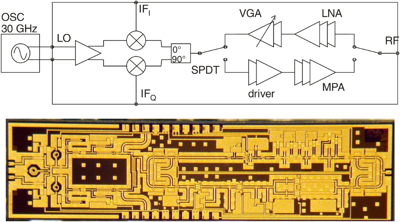
Fig. 6. Chip photograph and block diagram of the fully integrated I/Q transceiver MMIC.
A) Receiver
To measure the transceiver in the receive case, an Agilent E8257 signal synthesizer with an attached HP 83557 source module provides the RF signal in the frequency range up to 67 GHz. The 30 GHz LO signal is provided by a second signal synthesizer. The down-converted IF signal is fed via a coaxial cable to a spectrum analyzer. Figure 7 shows a diagram of the employed measurement setup.
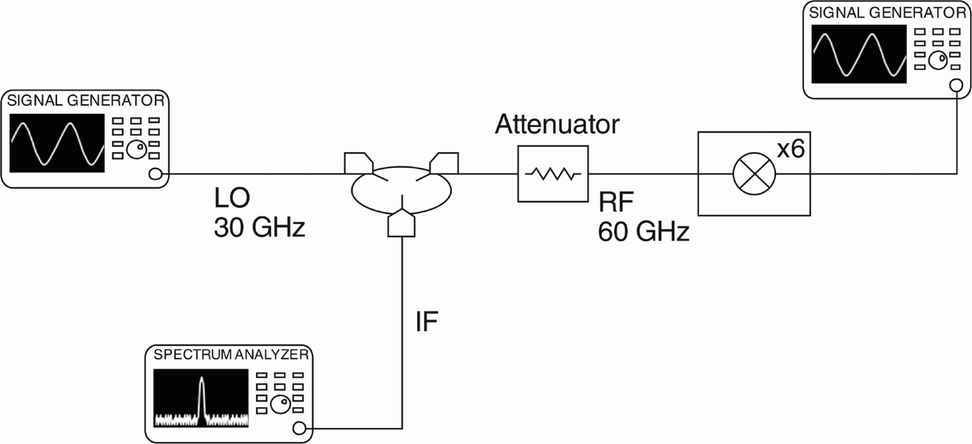
Fig. 7. Receiver measurement setup.
During the measurement only one IF output is measured, whereas the second output is terminated into a 50 Ω load. The RF signal is applied with a power level of −35 dBm using an additional attenuator in order to ensure linear receiver operation.
The measured performance is shown in Fig. 8. In down-conversion mode, the transceiver achieves a maximum conversion gain of 16.3 dB with 0 dBm LO power applied in the IF-I branch (Fig. 8(a)). The measurements versus the RF frequency (Fig. 8(b)) have been executed at a constant LO power level of −1 dBm. The conversion gain of the IF-I and the IF-Q branch stays between 16.3 and 12.4 dB from 55 to 65 GHz.

Fig. 8. Conversion gain of the receiver over LO power (a) and RF frequency (b).
The I/Q phase difference is of particular interest in digital communication where phase-modulated signals like Quadrature Phase-Shift Keying (QPSK) or Quadrature Amplitude Modulation (QAM) are widely used to achieve high data rates. It is therefore necessary to achieve a fixed 90° phase shift between the I and the Q branch of the transceiver. Figure 9 shows the phase difference as a function of the applied LO power. It can be seen that the I/Q phase is sensitive to the LO power level and 89° phase difference is achieved for 0 dBm LO power.

Fig. 9. Phase difference between the I and the Q branches versus the applied LO power.
B) Transmitter
In the transmit case, the IF signal is injected by a signal synthesizer at a frequency of 100 MHz. The LO signal preparation is the same as in the receive case. At the RF output, we connect a V-band mixer to observe the up-converted signals in a spectrum analyzer. That way, we can separately measure the signal strength at the RF frequency (measurements are shown at the lower sideband only) and at the second LO harmonic. The latter measurement allows the assessment of the LO-to-RF isolation during up-conversion. Figure 10 shows the described measurement setup.

Fig. 10. Transmitter measurement setup.
The measured performance is shown in Fig. 11. The up-converter achieves a maximum output power of more than 12.3 dBm with 2 dBm LO power applied (Fig. 11(a)). The LO-to-RF isolation increases with higher LO power and reaches 23.3 dB, also at 2 dBm LO power.

Fig. 11. RF output power and LO-to-RF isolation of the transmitter versus LO power (a) and RF frequency (b).
Figure 11(b) shows the measured output power and corresponding LO-to-RF isolation for a fixed LO power level of −4 dBm. The output power for this LO level stays between 5.5 and 10.4 dBm from 55 to 65 GHz.
VIII. CONCLUSION
Broadband 60 GHz analog frontend building blocks and integrated transceiver MMICs have been successfully realized in a 100 nm mHEMT technology. The MMICs are dedicated to the hybrid combination with subsequent Si-based components to form high-performance 60 GHz frontends. The LNA achieves a measured small-signal gain of more than 20 dB with a noise figure of <2.5 dB. The integrated medium power amplifier delivers a saturated output power of 20 dBm and features a small-signal gain of 20 dB from 55 to 65 GHz. A combination of the LNA, MPA, and antenna switch achieves a measured noise figure of 4 dB and can be used as a high-performance 60 GHz extension to SiGe or CMOS chips. Finally, a fully integrated single-chip transceiver with subharmonic LO injection achieved a measured conversion gain in the receive case of more than 15 dB. The measured transmit power of the transceiver exceeded 12 dBm with a measured LO-to-RF isolation of more than 20 dB.
ACKNOWLEDGEMENTS
The authors would like to thank their colleagues from the Fraunhofer IAF for excellent epitaxial growth and wafer processing. This work was supported by the German Federal Ministry of Education and Research (BMBF) and carried out in the frame of the EASY-A project.
 Daniel Lopez-Diaz was born in 1982. He received the Dipl.-Ing. degree from the University of Karlsruhe in 2008. He joined the Fraunhofer Institute for Applied Solid State Physics in Freiburg, Germany in 2009 for his doctoral thesis. His main research interests are the design of frequency conversion circuits above 200 GHz and millimeter-wave imaging.
 Ingmar Kallfass received the Dipl.-Ing. degree in electrical engineering from University of Stuttgart in 2000, and the Dr.-Ing. degree from University of Ulm in 2005. In 2001, he worked as a visiting researcher at the National University of Ireland, Dublin. In 2002, he joined the department of Electron Devices and Circuits of University of Ulm as a teaching and research assistant. In 2005, he joined the Fraunhofer Institute for Applied Solid State Physics with a focus on non-linear millimeter-wave integrated circuit design. Since June 2009, he is a professor at the Karlsruhe Institute of Technology in the field of high-speed integrated circuits.
 Axel Tessmann received the Dipl.-Ing. degree in electrical engineering from the University of Karlsruhe, Germany, in 1997 and the Ph.D. degree in electrical engineering from the University of Karlsruhe, Germany, in 2006. In 1997 he joined the High Frequency Devices and Circuits Department, Fraunhofer Institute for Applied Solid State Physics (IAF), Freiburg, Germany, where he is involved in the development of monolithically integrated circuits and subsystems for high-resolution imaging systems up to 500 GHz. His main research areas were the design and packaging of millimeter-wave ICs using high electron mobility transistors on GaAs, GaN, and InP as well as circuit simulation and linear and nonlinear device modeling. He is currently Group Leader of the millimeter-wave packaging and subsystem group at the Fraunhofer IAF.
 Rainer Weber was born in Offenburg, Germany, in 1978. He received the Dipl.-Ing. (FH) degree in electrical engineering from the University of Applied Sciences Offenburg, Germany, in 2003. He then joined the High Frequency Devices and Circuits Department of the Fraunhofer Institute for Applied Solid State Physics (IAF), Freiburg, Germany, where he is involved in the MMIC design of amplifiers, oscillators, and multipliers up to 325 GHz.
 Hermann Massler was born in Radolfzell, Germany, in 1965. He studied electrical engineering at the Technical University Karlsruhe where he graduated in 1993. While working on his diploma degree at the Kernforschungszentrum Karlsruhe (KfK) he did quasi-optical measurements at 140 GHz. He continued these studies as Research Assistant in the KfK for one more year. Since 1994 he has been with the Fraunhofer Institute for Applied Solid State Physics (IAF) in Freiburg working on transistor- and IC-characterization up to 500 GHz.
 Arnulf Leuther received the Dipl. Phys. degree and the PhD degree in physics from the Technical University of Aachen. He is with the Fraunhofer Institute for Applied Solid State Physics (IAF) since 1996. The major working area is the development of HEMT technologies for sensor and communication systems up to 600 GHz.
 Michael Schlechtweg received his Dipl.-Ing. degree in electrical engineering from the Technical University Darmstadt in 1982, and the Dr.-Ing. degree from the University of Kassel in 1989. He joined the Fraunhofer Institute for Applied Solid State Physics in Freiburg, Germany, working on the design of millimeter-wave integrated circuits, and on nonlinear characterization and modeling of active RF devices. In 1994, he became head of the simulation and modeling group at Fraunhofer IAF. Since 1996, he leads the RF devices and circuits department, focusing on the design and the characterization of devices and integrated circuits based on III–V compound semiconductors for RF applications, as well as the development of integrated circuits and modules for sensor and communication systems up to 500 GHz and above. Michael Schlechtweg received the Fraunhofer Prize in 1993, and the European Microwave Prize in 1998. He has co-authored about 200 scientific publications, and holds two patents.
 Oliver Ambacher received his Dipl.-Phys. and Dr. degrees with honors from the Ludwig-Maximilians and Technical University Munich, in 1989 and 1993, respectively. In 1993, he joined the Walter Schottky Institute of the TU-Munich to investigate the epitaxial growth of group-III nitrides based heterostructures. Since 1995 the research of his group is focused on fabrication of GaN-based devices as well as on the understanding of polarization induced effects in group-III nitride heterostructures and quantum wells. 1998/1999, he spent 1 year at Cornell University, Ithaca, NY, as an Alexander von Humboldt fellow, where he was involved in the optimization of polarization induced AlGaN/GaN HEMTs for high-frequency and high-power applications. He became a professor of Nanotechnology and head of the Institute for Solid State Electronics located at the Technical University of Ilmenau in 2002. In 2004 he was elected as head of the new Center of Micro- and Nanotechnologies. Since 2007 he is the Director of the Fraunhofer Institute of Applied Solid State Physics and Professor for Compound Microsystems in Freiburg, Germany.


