I. INTRODUCTION
Nowadays, there is a growing demand for large data rates in wireless networks. Moving toward transfer rates with magnitudes of gigabits per second (Gbs) supposes a tremendous challenge, as this can only be accomplished by either increasing the spectral efficiency of the transmission or moving into higher-frequency bands, in the millimeter-wave region, which were not used for mobile communication so far. Currently, there is a lively discussion about using the 60 GHz band for applications that require high data rates [Reference Smulders1–4]. The Easy-A project [5], partly funded by the German Ministry of Education and Research (BMBF), investigates efficient systems and concepts for the implementation of a 60 GHz t for video streaming in an aircraft or vehicle and fast wireless data synchronization links for consumer applications. In this context, it is necessary to develop highly integrated transceiver front-ends that can be easily and unobtrusive embedded in different devices, to respond to the needs of various communication scenarios.
This paper deals with the work carried out by several partners within the EASY-A project. The aim is to develop compact front-ends that include the IF and RF circuitry as well as their associated antennas for future 60 GHz communications equipment.
II. ANTENNA SUBSYSTEM: DESIGN CHALLENGES
Moving up in frequency implies facing new challenges associated with the design of RF circuits in general, and antenna subsystems in particular. Indeed, as the size of the elements becomes smaller, design and fabrication tolerances may turn out to be decisive. For the 60 GHz band and in particular for the examined antennas, the following issues have been identified as critical:
– Bandwidth: The considered frequency band extends from 56.7 to 66.5 GHz. Four bands are available within this range, each of them covering approximately 2 GHz of bandwidth. Should one antenna element be designed to cover the whole band of approximately 10 GHz or 15% relative bandwidth, the design would become highly challenging, surely due to the manufacturing tolerances that play a major role at 60 GHz. Such tolerances can only be counteracted by accurately analyzing the type of variations, and taking these into account for the design of the antenna element.
– Cost-effective integration: The final aim is to suggest a solution that offers the prospects of a cost-effective product. This implies that a high degree of integration is desired, especially with the other microwave components. Antenna build-ups requiring multiple external components or complex geometrical shapes were discarded, as they would complicate the production.
– Polarization: Circular polarization (CP) offers advantages in ease of antenna alignment and in interference suppression under adverse line-of-sight conditions. On the other hand, for environments with rich multipath propagation characteristics, the CP could degrade the resolvable received signal, due to random polarization changes that occur to its turning direction.
– Single versus dual polarization: With dual polarization, two independent channels can be used to carry the same information. Both signals are then variably summed at the receive end to avoid polarity-specific fading. Alternatively, if a more complex signal processing hardware is employed, the channels can carry different information so that the capacity of the link is doubled (e.g. using Multiple-Input, Multiple-Output (MIMO) techniques). In the former case, there are additional advantages in ease of antenna alignment and elimination of interference by reflected signals. Employment of dual polarization is limited by the degree of cross-polar discrimination that is achieved by the antenna equipment and cross-polar cancelation technology.
– Antenna arrays: In order to increase the gain and to shape the radiation pattern to cover the user scenarios, the antenna elements can be grouped into arrays. The required footprints of the radiation patterns for the different user scenarios will determine the actual size of the array. In general, the feeding network of the array will introduce additional losses, which on a typical low-temperature co-fired ceramics (LTCC) substrate at 60 GHz could add up to 1 dB/cm.
A number of literature references can be found which deal with antennas for the millimeter-wave applications at 60 GHz [Reference Lamminen, Säily and Vimpari6–Reference Franson11]. These include variations of the patch antenna, dipoles, Yagi, and Vivaldi antennas, which can be used for certain applications. Yet, some of them are hard to adapt to the problem considered here, due to their bandwidth, radiation patterns, and their orientation with respect to the carrier plane or fabrication issues.
Two different scenarios were considered: ultra-high rate – cordless (UHR-C) for high-capacity short links and very high rate – extended range (VHR-E) for large data rate Wireless Local Area Networks (WLAN). The profiles for the two different scenarios differ in general only in polarization type (linear, circular, or dual) and beamwidth, and address approximately the same bandwidth. The EASY-A project includes the design of the antennas for both the “tag” (that is, the “mobile” station) and the access points (AP) in the foreseen environments.
III. ULTRA-HIGH RATE – CORDLESS
A) Antenna requirements
The first scenario that was considered was UHR-C, for the fast exchange of information over short link in indoor environments, for example, for medical devices. UHR-C wireless communication systems require a data rate of several gigabits per second data rate, which puts stringent requirements on the antenna bandwidth. A desired antenna solution should meet the following equally important design objectives (see Table 1):
– The antenna bandwidth should cover 9 GHz to enable all possible applications worldwide, from 57 to 66 GHz [Reference Estañ, Branković, Dombrowski and Radović12]. Yet, one single channel is only 2 GHz wide. There is the possibility of implementing channel bonding, which means using two adjacent channels simultaneously to increase the data rate.
– Type I antennas will take the form of a small array with a pencil-beam pattern, and a gain of at least 12 dBi.
– Type II antennas will be linear arrays with hemispherical coverage and a minimum gain of 5 dBi.
– Low cost and robust to production tolerances.
Table 1. Design specifications for the antennas of the UHR-C prototypes.

Planar antennas (such as patches and printed dipoles) have drawn the attention in the last years than other conventional designs, due to numerous benefits that they bring to modern wireless systems [Reference Nesic, Nesic, Brankovic, Sasaki and Kawasaki13]. They have low profile and light weight. They are highly suitable for mobile applications, easy to integrate into arrays and with other electronic components, as well as compatible with IC technology. Furthermore, most of these antennas are manufactured with printed circuit techniques, and therefore, are very low cost. They are therefore good candidates to be used in 60 GHz UHR-C applications.
B) Antenna concepts
The antenna solutions developed for the 60 GHz band UHR-C prototypes are based on printed linearly polarized dipole elements. The four antenna types presented in this section consist of one-dimensional or two-dimensional dipole arrangements on a 127 µm-thick RT/Duroid 5880 substrate [14] that result in the desired radiation pattern and gain. RT/Duroid 5880 features a low dissipation factor (tan δ = 0.0009 at 10 GHz), and a dielectric permittivity at 10 GHz of 2.2 ± 0.02. The copper-foils metallization has 18 µm thickness, with a surface roughness of around 1.9 µm in the treated side and 0.4 µm in the untreated side.
In general, printed microstrip antennas show some drawbacks, such as narrow impedance bandwidth produced by the electrically thin ground-plane-backed dielectric substrate, which leads to a highly resonant behavior. Several techniques have been studied in order to increase the bandwidth of such antennas. One way would be to increase the substrate thickness, at the cost of poorer radiation efficiency. Alternatively, a substrate with a lower dielectric permittivity, parasitic elements, or optimized feeding methods can be used. In this specific case, the design aims at enhancing the impedance bandwidth by using a double-sided printed dipole antenna. This structure has proved to provide larger bandwidths than conventional configurations of microstrip patch antennas.
The proposed antennas are based on a double-side flat circular dipole structure. Such circular dipoles have been chosen not only for their broadband characteristics, but also for their satisfactory radiation properties. Some factors influence the performance of the circular dipole antenna, like the dimensions of the radiator element (discs), or the thickness of the metallization. Tapering matching techniques have been used to construct complex array structures. In order to connect the balanced antennas to coaxial cables (through coaxial connectors), exponential tapered baluns have been used as an impedance transformer network in the feeding sections of the circular antennas. The achieved impedance bandwidth of a single circular dipole lays around 20 GHz (from 55 to 76 GHz) with 100 Ω port impedance.
As indicated in the previous section, two different designs have been studied to meet the specifications. Type I antennas were designed to provide a pencil-beam radiation pattern. The antenna elements that form the array are placed on a plane at some specific distance over a reflector that helps to increase the gain in the broadside direction. Two different arrays of 2 × 2 and 4 × 4 dipoles, respectively, have been designed and simulated; their structure is depicted in Fig. 1.

Fig. 1. Simulation model of the 2 × 2 and 4 × 4 circular dipoles arrays. The back side of the substrate is a full metal plate used as a reflector.
Type II antennas were designed to have maximum gain and radiation in the horizontal direction (the plane of antenna substrate). Here again, two concepts, with different number of single elements (dipoles), were chosen. In this case the elements form a linear array but the position and shape of the reflector is different. The reflector under the circular patch is etched on the copper of the bottom side of the substrate, and has a parabolic shape, as can be seen in Fig. 2.

Fig. 2. Simulation model of the 2 × 2 and 4 × 4 arrays of dipole elements. The parabolic-shaped metallization on the back side of the substrate is used as reflector.
The feeding structure of both antenna types is printed on the same surface as the radiating elements, as sometimes the substrate used in the fabrication is not suitable for processing the vias needed for probe feeding. Aperture-coupling and proximity coupling feeds would require the use of multilayer substrates such as LTCC or liquid crystal polymer, which can increase the complexity of the design. By printing the feeding network on the same surface as the elements, many of these complexities are eliminated. The feeding network implemented here consists of an equal power split T-junction where the 50 Ω line splits into two 100 Ω lines. Furthermore, the 100 Ω lines pass through the reflector before feeding the driven dipole elements.
For the simulation of the antennas, Ansoft HFSS software has been used [15]. This software allows efficient and accurate numerical simulation of the electromagnetic behavior of complex structures using finite-element methods. For all analysis, the center frequency of 62 GHz has been used in order to calculate fields and meshing. The resulting radiation patterns of all antenna types are given in Figs 3–6. The patterns show that the shape and the maximum gain fulfill the expectations.

Fig. 3. Simulated radiation pattern of the Type II array with 2 × 1 elements (E θ, φ = 0°, 90°).

Fig. 4. Simulated radiation pattern of the Type II array with 4 × 1 elements (E θ, φ = 0°, 90°).

Fig. 5. Simulated radiation pattern of the Type I array with 2 × 2 elements (E θ, φ = 0°, 90°).

Fig. 6. Simulated radiation pattern of antenna with 4 × 4 dipole elements (E θ, φ = 0°, 90°).
All four antenna types have been fabricated. The prototypes are shown in Fig. 7. V-connectors (V103F Anritsu, [16]) were used to feed the antennas. Holders were added to adapt them to the measurement setup. The size of the biggest antenna holder is 3 cm ×3 cm, while the antenna itself is less than 2 cm × 2 cm. A conductive two-part epoxy silver glue has been used to fix the antennas to the holders to provide the lower ohmic contact possible to the ground. A network analyzer was used to measure the fabricated antennas up to 65 GHz. Both the measured and the simulation results are displayed in Figs 8 and 9. The effect of the V-connector could not be de-embedded, due to problems with the Thru-Reflect-Line (TRL) calibration standards available. Further analysis would be necessary to determine the exact contribution of both the connectors and the calibration on the measurement errors. Nevertheless, it still can be appreciated how the bandwidth requirements are matched.

Fig. 7. The four antenna prototypes mounted on holders with V-connectors.

Fig. 8. Simulated and measured reflection coefficient (S11) versus frequency for Type II arrays. 2 × 1 (left) and 2 × 2 (right).

Fig. 9. Simulated and measured reflection coefficient (S11) versus frequency for Type I arrays. 4 × 1 (left) and 4 × 4 (right).
The radiation patterns of the arrays were measured at IMST GmbH. A comparison between simulated and measured results is provided in Table 2. The noticeable gain difference in some of the samples measured is due to the effect of the sensitive assembly with the V-connector, and tolerances in the fabrication of the samples (the distance between the antenna and reflector is not exactly the same as in the simulations). By extrapolating the results of the measurements, a gain of 21 dBi is expected for an 8 × 8 array, at the cost of a larger area.
Table 2. UHR-C antennas – simulation and measurement results.

The 4 × 4 array displays very good agreement between simulated and measured values for gain and radiation pattern, as can be seen in Fig. 10. The slight deviation of the main beam is due to the asymmetry in the position of the antenna with respect to the ground plane, and the effect of the feeding lines and connectors.

Fig. 10. Measured radiation pattern of the 4 × 4 elements array antenna at frequencies from 57.5 to 63 GHz.
IV. VERY HIGH RATE – EXTENDED RANGE
One of the aims of the EASY-A project is to analyze the integration of the antennas and the RF front-end. The goal is to explore the feasibility of combining the microwave chips, the circuitry, and the antennas on the same LTCC module. This research was carried out taking into account a VHR-E scenario, in this case, a high-data rate WLAN for in flight entertainment.
A) Requirements
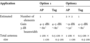
Table 3 shows different design specifications for the prototypes of the VHR-E prototypes, with different degrees of complexity, to cover a wide spectrum of applications. The frequency band of interest was limited in these first prototypes to the band between 59.5 and 62 GHz, which is available worldwide for 60 GHz unlicensed applications. The three different options display the following characteristics:
– Option 1: the simplest solution consists of a single radiating element both in the tag and the access point, with single linear polarization, for measurement purposes.
– Option 2: Single elements or small arrays with single linear polarization, which can be integrated in the RF package.
Table 3. Preliminary design specifications for the antennas of the VHR-E prototypes.

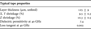
Two different types of antenna elements were analyzed and fabricated for the VHR-E scenario, namely radiating patches and cavities. In both cases, the antennas were fabricated using LTCC substrate. Specifically, the 943 Low-Loss Green TapeTM from DuPont was selected [17]. Its main nominal characteristics are listed in Table 4. During the process, it was observed that some adjustments had to be made to compensate for material tolerances and for the deviation of the tape properties from the nominal ones [Reference Oikonomopoulos-Zachos and Martínez-Vázquez18]. These deviations were observed in all the prototypes fabricated during the project, for the all examined antennas.
Table 4. DuPont 943 substrate main properties [17].
B) Patch antennas
Planar patch antennas appear well suited for the given scenarios, due to the compact hybrid integration of the transceiver front-ends and the main lobe pointing perpendicular to the substrate carrier. Aperture coupling was the method of choice for the antenna feed [Reference Zürcher and Gardiol19], as a fractional bandwidth of 15% had to be achieved to cover the complete frequency band from 57 to 66 GHz. A direct feed approach utilized in earlier works did not provide sufficient bandwidth for the application at hand, especially on the high-permittivity substrates used in LTCC processes (εr ≈ 7–8, see Table 4) [Reference Alhouri, Rentsch, Stephan, Trabert, Müller and Hein20]. Both 2 × 2 and 2 × 1 array arrangements were investigated, in order to keep the link budget balanced, while reserving some margin for the length of the feeding transmission lines as well as for the losses of the bond wires.
Avoiding the use of vias for the actual radiating elements is an important advantage of patch radiators. Indeed, the influence of potential shifts between the via layers and the metallization layers on the antenna parameters is eliminated. Simulations have determined that the larger effect of fabrication tolerances on the performance of the antennas is due to shifts between the slot layer and the stripline layer and, to a lesser degree, to shifts between the slot layer.
For the coupling aperture, different options have been considered. Variations of the 2 × 2 array with rectangular slots (see Fig. 11) and H-shaped slots were designed and manufactured. For the 2 × 1 array only rectangular slots were investigated. While both aperture types exhibited a similar impedance bandwidth according to the simulations, the rectangular slot proved to be more robust against fabrication tolerances, especially layer shifts. Simulations also revealed that for the rectangular slots a coupling via open stub provided the largest possible bandwidth, while for the H-shaped slots a shorted stub was preferable.

Fig. 11. Left: 2 × 2 array configuration with metallic walls consisting of via fences. Right: simulated influence of the metallic via fence on gain versus frequency.
As the realization of 50 Ω striplines would result in structural dimensions of less than 60 µm, which was proved not to be reliable for buried layers within the technology constraints, a more conservative stripline width of 100 µm was chosen, resulting in a characteristic impedance of 36 Ω.
Patches on dielectric substrates are subject to excitation of parasitic substrate waves, which generally propagate along the surface [Reference Zürcher and Gardiol19]. These waves cause unwanted radiation from the edges of the dielectric, reducing the gain of the main lobe of the patch antenna, and thus its radiation efficiency. Furthermore, the coupling between adjacent transmission lines can be enhanced unintentionally. All of the proposed designs hence employ an approach to reduce this parasitic radiation utilizing a grounded via fence around the antenna arrays. The influence of this design measure on the gain of the 2 × 2 array is displayed in Fig. 11, keeping the gain of the antenna above 10 dBi up to 65 GHz. Without the fence the gain rapidly decreases above 59 GHz.
Since all antennas were designed for integration with differential monolithic microwave-integrated circuits (MMICs), a balun had to be included, in order to enable separate measurement access to the antenna for its characterization. While rat-race couplers were considered due to their favorable bandwidth, a less complex design with a T-junction balun was chosen. The structure of the balun is thoroughly explained in [Reference Wollenschläger, Stephan, Xia, Müller and Hein21].
The fabricated test antennas are displayed in Fig. 12. It can be observed that the structures differ from the ideal rectangular pattern due to the metallization process. Yet, this will have no significant effect on the antenna performance.

Fig. 12. Realized samplesof patch array antennas with gold metallization, manufactured for measurement purposes. The upper group is equipped with coaxial transitions while the lower group is equipped with waveguide transitions (access from the backside).
Some antennas were outfitted with a coaxial-to-stripline transition specifically designed for this measurement task, while a set of antennas utilized an already proven design of a waveguide-to-microstrip transition [Reference Wollenschläger22]. The waveguide-fed antennas exhibited distortions of the measured antenna patterns that can be attributed to the open microstrip stubs of the waveguide transition itself and the intermediary microstrip-to-stripline transition. Therefore, only the coaxial-fed test substrates were taken into account for the full antenna characterization.
The measured reflection coefficient of the 2 × 2 arrays is depicted in Fig. 13. The array with rectangular slots exhibited a −10 dB impedance bandwidth of 7 GHz, the H-shaped array featured 14 GHz of bandwidth, and the 2 × 1 array a matching bandwidth of 6 GHz. All frequency responses displayed resonances over the measured frequency range that could be attributed to the complex coaxial transition and long feed network.

Fig. 13. Simulated (red dashed curves) and measured (black solid curves) reflection coefficients (left-hand side) and gain versus frequency (right-hand side) of the patch arrays (top 2 × 2 array with rectangular slots, centre: 2 × 2 array with H-shaped slots, bottom; 2 × 1 array).
The radiation patterns were measured in the anechoic chamber of Ilmenau University of Technology, using a frequency conversion technique, more thoroughly explained in [Reference Wollenschläger22]. The results are shown in Figs 13 and 14. For the antenna with rectangular slots the gain remains above 10 dBi for frequencies between 58.5 and 64.5 GHz, while the antenna with H-shaped slots exhibits more than 9 dBi of gain between 57 and 65 GHz. While the latter design features a higher bandwidth and a better gain flatness, it is less efficient and provides less gain than the former. The gain of the 2 × 1 array is higher than 9 dBi between 59.5 and 62.5 GHz and exhibits a stronger frequency dependence than the 2 × 2 designs. The radiation patterns match well between simulations and measurements. For the integration into LTCC front-end modules, the 2 × 2 array with rectangular slots was eventually selected.

Fig. 14. Simulated (red dashed curves) and measured (black solid curves) radiation patterns of the measured antennas (top: 2 × 2 array with rectangular slots, centre: 2 × 2 array with H-shaped slots, bottom: 2 × 1 array).
C) Cavity antennas
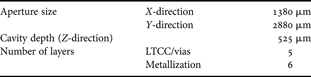
The second option investigated was the use of LTCC-filled radiating cavities, which behave as aperture antennas. The side walls of the cavities are realized with metal-filled vias, as shown in Fig. 15 [Reference Martínez-Vázquez, Holzwarth, Oikonomopoulos-Zachos and Rivera23]. A stripline is used as probe to excite the radiating modes in the cavity. The tapering of the cavity walls helps to improve the bandwidth, while the depth of the cavity determines the resonant frequency. This depth should be close to λ/4 of the design frequency. Five layers of material and thus six layers of metallization were needed for the optimum operation. The result is an asymmetrically fed, linear-polarized element with a maximum directivity of 5–6 dBi. The main characteristics of the resulting aperture antenna are listed in Table 5.

Fig. 15. Implementation of the aperture antenna. In the general view (left), the LTCC substrate is not fully shown for the sake of clarity. The red line represents the stripline feeding [Reference Martínez-Vázquez, Holzwarth, Oikonomopoulos-Zachos and Rivera23].
Table 5. Main physical characteristics of the aperture antenna.

For the implementation, the walls were defined by metal-filled via holes. Technological limitations impose a minimum distance of 350 µm between two vias. This distance represents around λ/6 in the substrate, and therefore the walls will not be completely impermeable to the electromagnetic waves at the operating frequencies. This in turn will have an important effect on the antenna performance and has to be carefully analyzed. The antenna is fed using striplines.
To obtain a symmetrically fed antenna array, two elements will be used in a 2 × 1 array configuration, as depicted in Fig. 16. In this case, the two sides of the array are excited with signals of opposite phases (0 and 180°), which can be obtained directly from the differential output of the foreseen transceiver chips. With this symmetrical feeding, it would be possible to optimize the power transfer between the differential RF transceivers and the radiating elements without using a balun. It can be observed that the mutual coupling between the elements and the feeding networks will have a strong influence on the antenna bandwidth.

Fig. 16. Symmetrically-fed 2 × 1 array (LTCC removed for clarity) [Reference Martínez-Vázquez, Holzwarth, Oikonomopoulos-Zachos and Rivera23].
The structure was simulated using the commercial EM solver EmpireTM [24]. Figure 17 shows the simulated reflection coefficient of the balance-fed antenna. Yet, like in the case of the patch arrays, the bandwidth is calculated using a reference impedance of 37 Ω. Indeed, the technology limitations for the width of the stripline do not allow the use of 50 Ω line. An impedance matching to 50 Ω will have to be implemented to connect the antenna to the RF front-end. Losses in the conductors and the LTCC substrate have been included in the simulations. A bandwidth of around 6.5 GHz (10.8%) is achieved if the antenna array alone is considered.

Fig. 17. Simulated reflection coefficient of 2 × 1 array.
The directivity of the 2 × 1 antenna array as an isolated element is shown in Fig. 18. A directivity value of around 8.5 dBi is obtained at the center of the frequency band, with a frequency stability of about ±0.5 dBi for the lower- and upper-band limits. Only the main component is shown, as the cross-polarization levels are extremely low.

Fig. 18. Simulated radiation pattern of 2 × 1 array, azimuth (left: E θ, φ = 0°, right: E φ, φ = 90°).
To measure the performance of the antennas, several prototypes with a waveguide transition on the backside (opposite to the antenna aperture) were designed and fabricated [Reference Martínez-Vázquez and Oikonomopoulos-Zachos25]. The structure of the transition is similar to that of the radiating elements, namely a tapered, LTCC-filled aperture. To match the structure to the waveguide, a cavity was etched in the LTCC. The signal from a standard WR-15 waveguide will thus be coupled to two striplines, with a phase difference of 180° between them, which is desired for the symmetrically fed antennas. This transition will have effects not only on the matching of the prototypes, due to the WR-15-to-stripline interface, but also on the radiation patterns, as the size of the antenna prototypes differs from that of the actual front-end.
Figure 19 displays a comparison between the results of the simulation of the whole structure (including WG-transition) and the measurements performed on two different antenna prototypes. Over 4 GHz impedance bandwidth is obtained with the 2 × 1 array, yet the results deviate from those predicted by the simulation. Although the measurements show a frequency shift with respect to the simulations, a bandwidth of around 5 GHz can still be achieved. This is very promising for the applications considered here. The reason of the discrepancies between simulation and measurements can be attributed to tolerances in the technological process, deviations in the material parameters with respect to the nominal values and the effect of the transition between the waveguide and the striplines.

Fig. 19. Reflection coefficients of the 2 × 1 array (including WG transition). Comparison between the FDTD simulation and the measurement of two different samples.
Discrepancies can also be observed in the radiation patterns, as shown in Fig. 20. Here, the effects of the ground plane and the flange can be observed. The achieved gain lays around 7 dBi, and is slightly lower than the simulated value.

Fig. 20. Measured radiation patterns of the 2 × 1 array with waveguide feeding. 2D cuts at 60 GHz.
V. LTCC MODULE AND INTEGRATION
One of the main aims of the project was to explore the feasibility of combining both the RF chips and circuitry and the antennas on the same LTCC module. The use of LTCC material allows for a high degree of integration with the RF circuits connected with such antennas.
A differential configuration was selected for the RF front-end, to combine with either patch or cavity (aperture) antennas. For both the TX and RX modules, the analog front-ends are connected to the antennas on the LTCC module. The differential output of the chip is connected to two parallel microstrip lines using wire bonding. The signals on the two lines have then a phase difference of 180°. Matching stubs are added to each of the signal paths to transform the impedances. In the case of the aperture antennas, the 50 Ω microstrip lines are then connected to the 37 Ω striplines of the antenna feeding network using a λ/4 impedance transformation. In Fig. 21, the interface between the RX- or TX- front-ends and the antennas is depicted.

Fig. 21. Simulation model of the transition between the MMIC and the antennas on the LTCC module.
The effect of the bond wires and matching circuit on the antenna performance were checked again using EmpireTM. The resulting 2 × 1 antenna array still shows a very large bandwidth in the simulation, as depicted in Fig. 22. The predicted gain lays around 8 dBi (see Fig. 23). This configuration yields in a half-power beamwidth of approximately 63° for φ = 0 and 71° for φ = 90°.

Fig. 22. Input reflection coefficient in dB of the 2 × 1 antenna array including the effect of the transition to the MMICs (bond wires, matching network, and microstrip-to-stripline interface).

Fig. 23. Simulated gain of the integrated 2 × 1 antenna array integrated in the LTCC module, including the effect of bond wires, matching networks, and transitions.
The final module (TX) is shown in Fig. 24. The total size is 25.2 mm × 29.5 mm, which is small enough for its integration for the desired applications such as on-board entertainment systems.

Fig. 24. Model and implementation of the complete RF-front-end (Tx-Module).
Once the modules have been fabricated, a final step is required for the characterization of the prototypes. Different elements have to be mounted and connected in order for the transceivers to be operated. Figure 25 illustrates the packaging of the RF-front-end for the RX- and TX-modules. Each system consists of three different parts:
– LTCC front-end, including the RF- and IF-chips, the antenna, and the blocking capacitors: The 60 and the 5 GHz IF chips are buried in a cavity of the LTCC substrate, and are additionally shielded. The antenna aperture is located on the opposite side of the LTCC.
– PCB interface board around the LTCC, using FR4 material, to accommodate the elements needed for the tests: Baluns, pin-connectors, level-shifter, trimmer, reset-button, and SMA-connectors for the single-ended baseband signal and the reference oscillator signal, as shown in Fig. 25. Blocking capacitors and test pins are also placed on this interface board.
– A heat-sink located on the back side of the module.

Fig. 25. Tx-LTCC-front-end with passive cooling element.
Figure 26 shows the final implementation of the RF front-end, including the FR4 interface board and the different connectors. In the final prototype, the complete RF circuitry is housed in a metal box that acts as an RF-shield. This shielding has been removed in the picture to allow the view of the different components.

Fig. 26. Implementation of a front-end with test-board.
VI. CONCLUSION
Different antenna solutions for highly integrated RF front-ends were analyzed and fabricated within the EASY-A project. They all show good performance, which fulfill the requirements for the different application scenarios, namely UHR-C and VHR-E. The integration of the antennas into the RF-front-ends shows also very promising results. The antenna prototypes that were fabricated display both small size and good behavior. Yet, it is necessary to connect the transceivers to an external board with additional elements, for its operation and tests. The optimization of the LTCC transceiver modules, in order to include a combined IF-RF chip on a single board, as well as all the necessary circuits and connectors for its operation without any additional interface board, are parts of the future work of the EASY-A project.
ACKNOWLEDGEMENTS
This work has been partially funded by the German Federal Ministry of Education and Research (BMBF) trough grant number 01BU0807 (EASY-A).
 Marta Martínez-Vázquez was born in Santiago de Compostela, Spain, in 1973. She obtained her engineer and Ph.D. degrees in telecommunications from the Universidad Politécnica de Valencia, Spain, in 1997 and 2003. The later was received a Best Ph.D. award (2004). Since 2000, she works for IMST GmbH (Germany). Her research includes mobile communications antennas, planar arrays, radar sensors, and RF systems. She is a member of the Administrative Committee of the Antennas & Propagation Society of IEEE, the Board of Directors of the European Association of Antennas and Propagation (EurAAP), and the Technical Advisory Panel for the AP Professional Network of IET. She has over 50 publications, including book chapters, journal, and conference papers and patents. She serves as a distinguished lecturer for the IEEE AP-S, an associate editor of “Antennas and Wireless Propagation Letters” and a member of the editorial board of the “Radioengineering” Journal.
 Christos Oikonomopoulos-Zachos was born in Volos, Greece, in 1976. He obtained both his Dipl.-Ing. and Ph.D. degrees in electrical engineering from the RWTH Aachen University, Germany, in 2003 and 2010, respectively. From 2003 until 2008 he worked as a scientific assistant in the department of High Frequency Technology of the same University. Since 2009 he is with the department of Antennas and EM Modelling of IMST GmbH. His current interests include MIMO antenna systems, LTCC technology, mobile communications antennas, and automotive antennas. He is the author of several papers in scientific conferences and journals.
 Kai Maulwurf was born in Wesel, Germany, in 1980. He received his diploma degree in electrical engineering from the Rheinische Fachhochschule Köln, Germany, in 2005. He is currently working in the RF-Modules Group of the Department of RF Circuits and System Integration of IMST GmbH in Kamp-Lintfort, Germany. His work includes the design, simulation, and measurements of analog front-end modules up to 77 GHz, for communication systems and radar applications.
 Frank Wollenschläger received his Dipl.-Ing. degree in theoretical electrical engineering in 2008 from Ilmenau University of Technology. He joined the RF and Microwaves Laboratory at Ilmenau University of Technology in 2008, where his research focuses on modeling and simulation of planar millimeter-wave antennas and their implementation on multilayer ceramics technology.
 Ralf Stephan was born in Erfurt, Germany in 1959. He received the Dipl. Ing. and the Dr. Ing. degrees in theoretical electrical engineering from the Technical University of Ilmenau in 1982 and 1987, respectively. From 1982 to 1989 he worked in the field of RF semiconductor modeling and circuit analysis. In 1987 he joined the RF and Microwave Lab of the Ilmenau University. Here he worked in the development of CAD tools, in the design of integrated GaAS circuits, and was responsible for the development of a noise radar demonstrator. His recent research interests include modeling of microwave circuits and systems, antenna measurement, antenna design, and EM field analysis.
 Matthias A. Hein received his diploma and doctoral degrees with honors from the Bergische Universität Wuppertal, Germany, in 1987 and 1992, respectively. His research there dealt with metal and oxide superconductors for microwave applications. In 1999, he received a British Senior Research Fellowship of the EPSRC at the University of Birmingham, UK. From 1998 until 2001, he headed an interdisciplinary research group focusing on passive microwave devices. In 2002, he joined Ilmenau University of Technology as Head of the RF and Microwave Research Laboratory. He currently leads the Institute for Information Technology. He has authored and coauthored about 340 publications, provided over 30 invited talks and tutorials at international conferences, and supervised over 60 diploma and doctoral students. He acts as a referee for high-ranking scientific journals and international funding agencies. His research interests concern device, system, and measurement aspects of antennas, high-efficiency amplifiers, and sensors for various applications.
 Lei Xia was born in Shandong, China, in 1976. He received the B.S. degree in physical electronics in 1998, and M.Eng. and Ph.D. degrees in microwave engineering from the University of Electronic Science and Technology of China, Chengdu, China, in 2004 and 2008, respectively. He is currently a project researcher with the Department of Electronic Technology, Ilmenau University of Technology, Ilmenau, Germany. His research interests include LTCC RF circuits and package, microwave and millimeter-wave systems for wireless communication applications.
 Jens Müller received his diploma degree for electrical engineering and the doctoral degree from Ilmenau University of Technology, Ilmenau, Germany, in 1992 and 1997, respectively. From 1997 to 2005, he held managing positions in development departments at Micro Systems Engineering GmbH, Berg, Germany. In 2005, he returned to Ilmenau University of Technology to establish the junior research group “Functionalised Peripherics”. In July 2008 he was assigned full professor for the department of Electronics Technology at the same university. His research interest covers functional integration for ceramic based System-in-Packages considering aspects of harsh environmental use, and high thermal/high-frequency requirements.
 Carlos Estañ Requeni received the B.S. and M.S. degrees in telecommunication and electronics engineering from Ramón Llull University (La Salle Engineering, Barcelona, Spain) in 1997 and 2001, respectively. In 2004 he received the M.S. degree in microsystems engineering from University of Applied Sciences Furtwangen (Germany). From 1999 to 2002 he worked as a software engineer at ENDESA Servicios SL (Control Systems Development Centre), Barcelona. From 2004 to 2005 he worked as a microsystems engineer at the IAF (Institute for Applied Research) at HS-Furtwangen (Germany). Since 2005 he is working for TES Electronic Solutions GmbH (Stuttgart, Germany) as an Analog/RF IC and antenna designer.
 Kai F. Dombrowski received his masters degree in physics from the University of Freiburg, Germany, in 1996 and his doctorate from the Technical University Cottbus, in 2000. He has since been involved in the design of broadband wireless systems for local area networks and body area networks. For several years, he has managed research projects providing innovative system and protocol solutions for body area network application scenarios. He has been involved in the development of ultra-wide-band (UWB) technology since the beginning of standardization in 2002 and has now moved on to the design of multi-gigabit systems at 60 GHz. He has authored and co-authored more than 20 scientific papers and several patent applications. He joined TES Electronic Solutions GmbH in 2005 as technical leader for wireless system and protocol design. Since 2010 he is responsible for wireless and graphics IP developments within TES as Director of Technology Development.
 Veselin Branković received his Dr.-Ing. (Ph.D.) from the University of Bremen in 1995. He is now Director Hardware Platforms in TES Electronics Solutions GmbH, Stuttgart. His activities cover technology and solution designs for industrial, defence, avionics, high end consumer, and telco markets. Since 1996 Dr. Branković works on advanced 60 GHz technologies. He is author and co-author of 29 granted patents, about 40 papers and holder of several Sony advanced research awards.
 Dušan Radović was born in Kosovska Mitrovica, Serbia, in 1975. He earned his Dipl.-Ing. (MSEE) in 1999 from the University of Belgrade, Serbia. Till 2001 he worked on aircraft noise measurement at the Flight Test Centre in Belgrade. After that, he worked as R&D engineer in the Institute Michael Pupin in Belgrade till 2004. From 2004 till 2006, he was with ELSYS Eastern Europe in Belgrade. He joined TES Electronic Solutions GmbH in Stuttgart in 2006. His expertise includes 60 GHz system development and design of IR UWB- and OFDM-based systems. He authored and co-authored around 30 papers on communications and signal processing topics.