I. INTRODUCTION
Rat-race coupler (RRC) or 180° hybrid is a simple and popular component used extensively in the design of power dividers/combiners, Butler matrixes, mixers, phase shifters, power amplifiers, antenna feeding networks, etc. [Reference Pozar1]. It provides equal or unequal power division with a 0°/180° phase at designated outputs and offers perfect isolation between the output ports. Another important property of RRC is that, it can add or subtract two input signals. In spite of the many advantages and applications, the large circuit area requirement especially at lower microwave frequencies and higher-order harmonics are the inherent drawbacks of the conventional RRC. Different approaches such as stub-loaded transmission lines [Reference Nie, Luo, Guo and Fan2, Reference Mondal and Chakrabarty3], low-pass filter unit cell (LUC) [Reference Song, Deguchi and Tsuji4], and meandering technique [Reference He and Wang5, Reference Awida, Safwat and El-Hennawy6] have been reported to reduce the size and improve the harmonic suppression capability of the RRCs. Next, to meet the wideband requirement of modern communication systems, microwave devices with wide bandwidth and compact size are in demand. Several techniques have been proposed to improve the bandwidth of RRC at the cost of increased design complexity and/or circuit size [Reference Ang, Leong and Lee7–Reference Mohyuddin, Kim, Woo, Choi and Kim18]. The design complexity includes multilayer, via-holes, slots, tight coupling, lumped elements, etc. Two single stage RRCs are cascaded in [Reference Ang, Leong and Lee7] to achieve 50% bandwidth. The drawback of the proposed design is that, it has crossovers implemented by soldering strips of copper tape across the microstrip traces. A novel wideband multi-section 180° hybrids using vertically installed planar coupler with bandwidth above 85% are reported in [Reference Chi and Chang8]. However, installation of vertical substrate complicates the fabrication. Even though, techniques such as left-handed transmission line sections [Reference Sorocki, Piekarz, Wincza and Gruszczynski9], coupled lines, and impedance transformers [Reference Gruszczynski and Wincza10] improve the bandwidth of RRCs to a greater extent, they occupy a very large area and need multilayer realization. In [Reference Taravati11], the branches of the conventional RRC are replaced using non-uniform microstrip transmission line sections for wideband operation. In some of the reported works, phase inverters are used to realize broadband 180° hybrids [Reference Kim, Song and Kim12, Reference Mung and Chan16–Reference Mohyuddin, Kim, Woo, Choi and Kim18]. The phase inverter provides a wideband 180° phase shift by reversing the signal and ground line. The design of RRC using phase inverter includes via-holes and ground slots. A conventional two-stage RRC without any plated through holes, slots or bonding wires with 50% bandwidth is reported in [Reference Caillet, Clénet, Sharaiha and Antar14] and the size of the RRC is reduced by 69% using the space filling curves. A wideband 180° hybrid coupler using symmetrical four strip interdigitated coupler is presented in [Reference Jung15]. This coupler has 10 dB return loss bandwidth of 62% and the relative circuit area is 40% of the conventional coupler. Most of the reported wideband RRCs are implemented using distributed elements and these designs will have higher-order harmonics, which adversely affect the system performance, but none of these have shown the harmonic suppression ability. To cope up with the higher demands of modern communication systems, devices with compact size, large bandwidth and harmonic suppression are needed. Therefore, still it is an open challenge for the current researchers to design the RRCs with high miniaturization, large bandwidth, and wideband harmonic suppression.
In this paper, a series stepped-impedance transmission line, center tapped with a shunt stepped-impedance open stub, is proposed for size miniaturization and harmonic suppression. Stepped-impedance transmission lines are used to design and reduce the size of many microwave devices such as RRC [Reference Kuo, Wu and Chiou19], power divider [Reference Sedighy and Khalaj-Amirhosseini20], dual-band couplers [Reference Chin, Lin, Wei, Tseng and Yang21], and filters [Reference Gómez-García, Muñoz-Ferreras and Sánchez-Renedo22, Reference Velidi, Guntupalli and Sanyal23]. The series stepped-impedance line and stepped-impedance shunt stub are combined in this work and a detailed study of effect on the magnitude response of the structure is carried out by varying the electrical lengths. The proposed structure along with the meandering technique is effectively used to design a highly compact wideband RRC. The designed double-section wideband coupler size is reduced by 86% with 50% bandwidth. The full-wave and measured responses show the harmonic suppression ability up to 5f 0, where f 0 is the operating frequency.
II. PROPOSED TRANSMISSION LINE ANALYSIS
Figure 1 shows the layout of the proposed series and shunt stepped-impedance transmission line (SSSITL). It consists of a pair of series transmission lines (Z 1, θ 1), (Z 2, θ 2), and a shunt stepped-impedance open stub with impedances Z H , ZL , and electrical lengths θ H , θL . To replace the conventional quarter wavelength transmission line (QWTL) with the proposed unit, the ABCD parameters of the conventional and the proposed SSSITL must be equated to obtain the equivalent impedance relations.
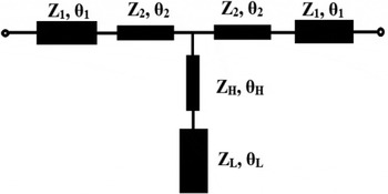
Fig. 1. Layout of the proposed SSSITL.
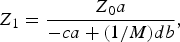
The ABCD parameters of the conventional QWTL is
 $$\left[ {\matrix{ {A_0} & {B_0} \cr {C_0} & {D_0} \cr}} \right] = \left[ {\matrix{ 0 & {jZ_0} \cr {\displaystyle{j \over {Z_0}}} & 0 \cr}} \right].$$
The ABCD parameters of the proposed SSSITL structure can be written as
 $$\left[ {\matrix{ A & B \cr C & D \cr}} \right] = S_1S_2S_3S_2S_1,$$
where S 1, S 2, and S 3 are used to denote the ABCD parameters of the series transmission lines (Z 1, θ 1), (Z 2, θ 2), and shunt stepped-impedance open stub, respectively and are given as
 $$\eqalign{& S_1 = \left[ {\matrix{ {\cos \theta _1} & {jZ_1\sin \theta _1} \cr {\displaystyle{{j\sin \theta _1} \over {Z_1}}} & {\cos \theta _1} \cr}} \right],\quad S_2 = \left[ {\matrix{ {\cos \theta _2} & {jZ_2\sin \theta _2} \cr {\displaystyle{{j\sin \theta _2} \over {Z_2}}} & {\cos \theta _2} \cr}} \right] \cr & \quad and \quad S_3 = \left[ {\matrix{ 1 & 0 \cr {\displaystyle{1 \over {Z_{in}}}} & 1 \cr}} \right]}$$
with
 $$Z_{in} = \displaystyle{{jZ_H(Z_H\tan \theta _H - Z_L\cot \theta _L)} \over {Z_H + Z_L\cot \theta _L\tan \theta _H}}.$$
By equating (1) and (2), assuming Z H = Z 2 and Z L = Z 1, the impedance relations are obtained as
 $$Z_1 = \displaystyle{{Z_0a} \over { - ca + (1{\rm /}M)db}},$$
 $$Z_2 = \displaystyle{{Z_0( - ea + fb)} \over a},$$
where
 $$M = \displaystyle{{Z_2} \over {Z_1}},$$
 $$a = \displaystyle{1 \over M}\cot \theta _L - \tan \theta _H,$$
 $$b = 1 + \displaystyle{1 \over M}\cot \theta _L\tan \theta _H,$$
 $$c = \left( {\displaystyle{1 \over M}{\sin} ^2\theta _1 - M\,{\cos} ^2\,\theta _1} \right)\sin 2\theta _2 - \sin 2\theta _1\cos 2\theta _2,$$
 $$\eqalign{d =& - M\sin 2\theta _1\sin \theta _2\cos \theta _2 - \sin ^2\theta _1\cos ^2\theta _2 \cr & - M^2\cos ^2\theta _1\sin ^2\theta_2,}$$
 $$e = (M^2\sin ^2\theta _1 - \cos ^2\theta _1)\sin 2\theta _2 - M\sin 2\theta _1\cos 2\theta _2,$$
 $$f = M^2\sin ^2\theta _1\sin ^2\theta _2 - \displaystyle{M \over 2}\sin 2\theta _1\sin 2\theta _2 + \cos ^2\theta _1\cos ^2\theta _2.$$
Equations (3) and (4) are solved graphically to obtain the equivalent impedances and electrical length θ 1 by assuming M, θ H , θL and θ 2 [Reference Velidi, Patel and Sanyal24]. For a QWTL with impedance Z 0 = 50 Ω, Fig. 2(a) shows Z 1 and Z 2 plotted against θ 1 for various impedance ratios M and considering other parameters as constant. As the impedance ratio M increases, the series electrical length decreases. The variation of equivalent impedances with respect to θ 1 for various electrical lengths θ H and θ L are shown in Fig. 2(b). The values of Z 2 are high when θ H < θ L . Similarly, Z 1 and Z 2 versus θ 1 for various electrical length ratio θ 2/θ 1 are shown in Fig. 2(c).
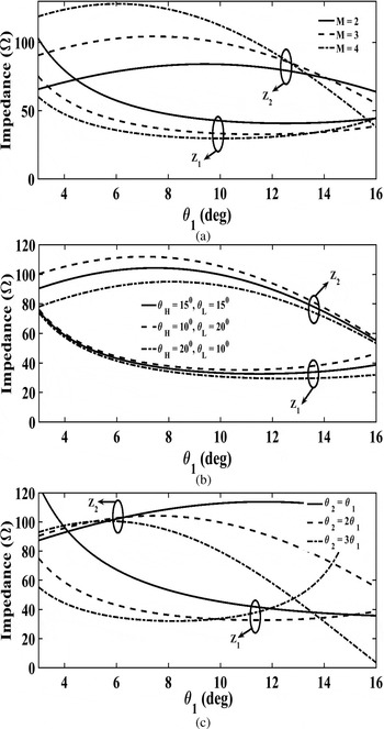
Fig. 2. Design curves for (a) Z 1 and Z 2 versus θ 1 for various M and fixed θ H = θ L = 15° and θ 2 = 2θ 1; (b) Z 1, Z 2 versus θ 1 for various θ H and θ L and fixed M = 3 and θ 2 = 2θ 1; (c) Z 1 and Z 2 versus θ 1 for various θ 2/θ 1 and fixed M = 3 and θ H = θ L = 15°.
The proposed SSSITL structure is compact when θ 1 + θ 2 < 45°. Considering M = 4, θ 2 = 2θ 1, θ H = θ L = 15°, the equivalent impedances and electrical length θ 1 for a QWTL with Z 0 = 50 Ω are Z 1 = 31 Ω, Z 2 = 124 Ω and θ 1 = 8.1°. The magnitude and phase responses of the conventional 50 Ω QWTL and its SSSITL equivalent are shown in Fig. 3. At the operating frequency, f 0 = 0.9 GHz, both the responses are matching. In addition to compactness, the equivalent SSSITL unit exhibits good band stop response beyond 1.5 GHz. Therefore, the proposed SSSITL can be utilized to design a compact and harmonic suppressed RRC.
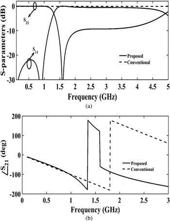
Fig. 3. Simulated frequency responses of the conventional 50 Ω QWTL and its proposed equivalent unit: (a) magnitude, (b) phase.
A) Effect of electrical length ratio θ 2/θ 1 on magnitude response
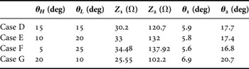
Considering M = 4, θ H = θ L = 15° and variable electrical length ratio θ 2/θ 1, the design parameters of the proposed SSSITL unit for Z 0 = 50 Ω are given in Table 1. The simulated magnitude response for each case is shown in Fig. 4. From the plot it is observed that, as the electrical length ratio is increasing, the stop band bandwidth is decreasing.
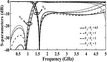
Fig. 4. Simulated magnitude response of the proposed structure for different electrical length ratio θ 2/θ 1.
Table 1. Design parameters of the proposed unit for different electrical length ratio θ 2/θ 1.

B) Effect of electrical lengths θ H and θ L on magnitude response
The electrical lengths θ H and θ L in case D of Table 1 are varied to study the effect on magnitude response of the proposed structure. For M = 4, θ 2/θ 1 = 3 and Z 0 = 50 Ω, Table 2 shows the design parameters by varying θ H and θ L . The simulated magnitude response for each case is shown in Fig. 5. From the plot it is observed that, when θ H is decreasing and θ L is increasing, there is an improvement in the band stop rejection and also in the bandwidth of the stop band.
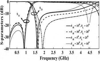
Fig. 5. Simulated magnitude response of the proposed structure for different electrical lengths θ H and θ L .
Table 2. Design parameters of the proposed unit for different electrical lengths θ H and θ L .
C) Advantage of the proposed SSSITL unit
The main structural advantage of the proposed SSSITL unit is that, the high impedance lines in the main line and shunt line can be meandered to avoid overlapping of stubs and also to achieve more compactness while realizing multi-section branch line couplers (BLCs) and RRCs. Figure 6 shows the layout of SSSITL with meandering the high impedance lines.

Fig. 6. Layout of SSSITL unit with meandering the high-impedance lines.
In case of multi-section BLCs [Reference Muracuchi, Yukitake and Naito25], the horizontal and vertical QWTLs are of low and high impedances, respectively. Structures like unequal length open stubs [Reference Velidi, Patel and Sanyal24], multiple symmetric pi-shape [Reference Barik, Phani Kumar and Karthikeyan26], and multiple asymmetric pi-shape [Reference Phani Kumar, Barik and Karthikeyan27] have been reported to replace the low-impedance horizontal QWTLs and the vertical high-impedance lines are meandered to obtain a compact topology, hence the unused space inside the coupler is well utilized by placing the meandered stubs, but in case of multi-section RRCs [Reference Caillet, Clénet, Sharaiha and Antar14], the conventional horizontal and vertical QWTLs are not very high-impedance lines, when attempted to replace these conventional lines with recently reported structures such as unequal length open stubs and multiple symmetric/asymmetric pi-shape, the horizontal and vertical equivalent unit shunt stubs will overlap and it is difficult to accommodate all the stubs inside the coupler, therefore making the coupler less compact. Basic structures such as T-shape [Reference Nie, Luo, Guo and Fan2] and Pi-shape [Reference Mondal and Chakrabarty3] are also not very much useful in realizing compact multi-section RRCs, since for low-impedance QWTLs, the equivalent shunt impedances are very low, hence it is difficult to meander them (because of larger line width) without overlapping or in other words it is difficult to achieve good size reduction (when the stubs are placed outside). Since the proposed SSSITL unit has high-impedance lines in series and shunt, these high-impedance lines can be meandered to avoid overlap and all the shunt stubs can be accommodated inside the unused space of the coupler, therefore more compactness can be obtained while realizing multi-section RRCs. In addition to compact topology, a band-stop response with different rejection levels can be obtained by varying the electrical parameters of the proposed structure and this is very much useful in suppressing the unwanted harmonics.
III. DESIGN OF COMPACT WIDEBAND DOUBLE-SECTION RRC USING SSSITL
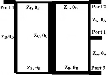
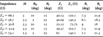
The bandwidth of RRC can be improved by cascading the sections. Figure 7 shows the layout of the double-section RRC [Reference Caillet, Clénet, Sharaiha and Antar14], where the impedances of the coupler have been optimized using a linear analysis tool, the circuit model of Ansoft designer. The optimized values are Z A = 66.1 Ω, Z B = 56.7 Ω, Z C = 30.8 Ω, Z D = 52.9 Ω, and Z E = 74.1 Ω for a 50 Ω port characteristic impedance. The electrical lengths θ A = θ B = θ E = 90° and θ C = θ D = 180°. This coupler occupies a large area of 0.51λ g × 0.51λ g , where λ g is the guided wavelength. The circuit size of the wideband coupler is drastically reduced by replacing the conventional QWTLs with the proposed SSSITL units. The 180° transmission lines are considered as two QWTLs for calculating the parameters. The design parameters of the equivalent SSSITL unit for each conventional line are shown in Table 3 and the circuit simulated response of the proposed coupler is shown in Fig. 8.

Fig. 7. Layout of the conventional double-section RRC.
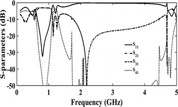
Fig. 8. Circuit simulated magnitude response of the proposed wideband RRC.
Table 3. Design parameters of the proposed broadband coupler.
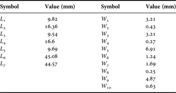
The wideband coupler operating at 0.9 GHz is designed, simulated using a full-wave simulator and fabricated on a Rogers RT/duroid 5870 substrate having ε r = 2.33, loss tangent = 0.0012 and substrate thickness of 0.787 mm. The layout and fabricated prototype of the coupler after replacing the QWTLs with SSSITL units are shown in Fig. 9. The dimensions of the final coupler design are given in Table 4.

Fig. 9. Proposed double-section RRC using SSSITL: (a) layout, (b) fabricated prototype.
Table 4. Dimensions of the proposed wideband 180° hybrid.
The proposed wideband coupler occupies an area of 4.45 × 4.81 cm2, which is 14% of the conventional coupler. R&S ZVL vector network analyzer is used to test the fabricated wideband double-section RRC. Figures 10 and 11 show the full-wave simulated and measured scattering parameters of the wideband RRC using SSSITL. At 0.9 GHz, the measured |S 21| is −3.5 dB, |S 31| is −3.42 dB, return loss is 21.02 dB and isolation is 21.43 dB. The 10 dB return loss (isolation) is from 0.69 (0.67) to 1.14 (1.24) GHz and the fractional bandwidth (FBW) is 50% (63.3%). The magnitude balance with in 0 ± 1 dB is from 0.69 to 1.15 GHz and the FBW is 51.1%. The measured in phase with 0° ± 1.5° is from 0.69 to 1.14 GHz and the out of phase with 180° ± 5° is from 0.7 to 1.15 GHz. Deviation between circuit predicted magnitude response (Fig. 8) and the full-wave simulated or measured responses (Fig. 10) is due to the coupling between the meandered series and shunt transmission lines.
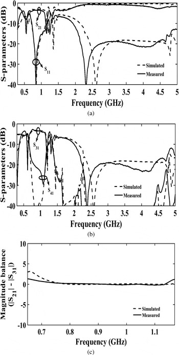
Fig. 10. Proposed double-section RRC full-wave simulated and measured magnitude responses: (a) S 11, S 21; (b) S 31, S 41; (c) balance (|S 21| − |S 31|).
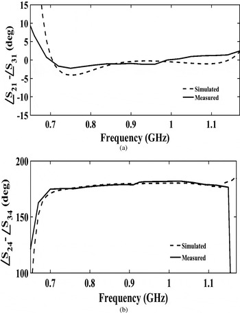
Fig. 11. Proposed double-section RRC full-wave simulated and measured phase difference responses at: (a) sum ports, (b) difference ports.
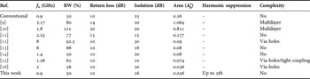
The performance of the proposed wideband coupler is compared with the other recently published works in Table 5. In spite of having wide bandwidth, the designs reported in [Reference Sorocki, Piekarz, Wincza and Gruszczynski9–Reference Taravati11] occupying very large area. Except [Reference Taravati11, Reference Abbosh13, Reference Caillet, Clénet, Sharaiha and Antar14], other works are having plated through holes which increase the fabrication cost and to the best of authors knowledge, there is no wideband RRC with harmonic suppression in the literature. The proposed wideband RRC is very compact and up to fifth harmonic is suppressed without any additional devices like low-pass filter, band stop filter, etc. The bandwidth of the proposed coupler can be still increased by cascading the sections and this is the best approach when compared with the complicated designs including multilayer, plated through holes, vertical substrate, bond wires, etc.
Table 5. Comparison with other reported broadband RRCs.
IV. CONCLUSION
A compact broadband double-section RRC is designed using newly proposed SSSITL units. The final layout of double-section RRC occupies 14% area of conventional coupler, along with harmonic suppression up to 5f 0, while exhibiting good input matching bandwidth. Design equations are derived using ABCD matrix formulation and solved graphically. As the proposed approach is based on transmission line theory, it is very much useful to design compact and harmonic suppressed devices.
ACKNOWLEDGEMENTS
The authors thank Dr. Vamsi Krishna Velidi, Scientist/Engineer- “SD”, Antenna & Passive Systems Division, Communication Systems Group, ISRO SATELLITE CENTRE, Bangalore for his valuable suggestions and encouragement throughout this work.
 Kanaparthi V. Phani Kumar received the B. Tech. degree in Electronics and Communication Engineering from Acharya Nagarjuna University, Guntur, AP, India in 2010 and the M. Des. degree in Electronic Systems from Indian Institute of Information Technology Design and Manufacturing (IIITDM), Kancheepuram, India in 2013. He is currently working toward the Ph.D. degree in Electronics Engineering at IIITDM, Kancheepuram, India. His research interests include microwave passive circuits and RFIC.
 S. S. Karthikeyan received the B.E. degree in Electronics and Communication Engineering from Bharathidasan University, Trichy, in 2001 and M.E. in Applied Electronics from Sathyabama University, Chennai, in 2005. He obtained his Doctoral Degree from the Indian Institute of Technology Guwahati, Assam, India in 2011. Currently he is working as an Assistant Professor at the Indian Institute of Information Technology, Design and Manufacturing Kancheepuram, Chennai, India. His research interests include electromagnetic bandgap structures, microwave filters, metamaterials, microwave sensors, etc.