


I. INTRODUCTION
Today, the AlGaN/GaN semiconductor material system is predominantly used to implement solid-state power amplifiers with high efficiency and output power at frequencies typically up to 20 GHz. High electron mobility transistors (HEMTs) realized on s.i. SiC substrates offer also excellent electronic properties for the next generation of solid-state microwave power amplifier in the mm-wave ([Reference Higaschiwaki, Minura and Matsui1–Reference Micovic4]). Recent advances of this technology demonstrated that substantial improvements in output power, power-added efficiency, and power density over other semiconductor technologies like GaAs and InP for W-band applications can be obtained. Typical saturated power levels achieved by various Monolithic Microwave Integrated Circuit (MMIC) technologies for a frequency range of 60–100 GHz can be seen in Fig. 1. Due to the larger bandgap of 3.4 eV and the corresponding high maximum field strength of about 3.0·106 V/cm compared to 1.4 eV and 0.4·106 V/cm for GaAs, GaN devices can be operated at much higher bias voltages. Furthermore, the good thermal conductivity of SiC substrates (up to 4.9 W/cmK compared to 0.46 W/cmK for GaAs) advocates the AlGaN/GaN technology for the operation at much higher power levels. Recently, output power levels of 31.1 dBm (1.3 W) at 75 GHz and 32.3 dBm (1.7 W) at 91 GHz were demonstrated based on GaN HEMT MMICs ([Reference Nakasha5, Reference Brown, Brown, Chen, Hwang, Kolias and Scott6]).

Fig. 1. Typical saturated MMIC power levels at 50–100 GHz.
This work demonstrates a dual-stage amplifier MMIC based on an AlGaN/GaN-HEMT technology with a gate length of 100 nm using dual-gate transistor structures to achieve a high output power and a high gain per stage. Dual-gate FETs have been applied successfully in a number of MMIC applications such as low-noise and power amplifiers [Reference Tessmann, Haydl, Hülsmann and Schlechtweg7]. As it is shown in this paper the dual-gate transistor yields a gain per stage of over 10 dB in the frequency range 58–67 GHz.
II. GAN DUAL-GATE-TECHNOLOGY AND PERFORMANCE
A) Dual-gate HEMT
The gate-drain capacitance of a common-source (CS) HEMT limitates essentially the maximum operating frequency of the active device. Thus, the bandwidth of the transistor is decreased by the increase in the equivalent input capacitance due to the voltage-inverting amplification of the HEMT. The negative feedback of the parasitic capacitance can be reduced by using a common-gate (CG) stage as a load for a CS HEMT. In this cascode amplifier configuration a higher bandwidth of the active devices can be achieved. Furthermore, the isolation and the gain per stage can be increased significantly by the application of the cascode. To save chip area the CS and the CG transistors can be embedded to one dual-gate HEMT without an additional transmission line between them. The gate-finger of the CG stage meshes into the CS transistor with the equivalent length and numbers of finger (nF) which also gives the total width of the cascode HEMT. The layout of an AlGaN/GaN dual-gate HEMT with a gate width of W G = 4×45 µm (nF CS = nF CG = 4; W F,CS = W F,CG = 45 µm) is illustrated in Fig. 2.

Fig. 2. Schematic (a) and chip image (b) of a coplanar dual-gate HEMT.
Due to the cascode configuration, three voltages are required for the biasing of the dual-gate HEMT. The gate-source voltage (V G) is applied at the first gate and the drain-source voltage (V D) at the drain of the CG-stage. The third is the voltage applied at the second gate of the dual-gate HEMT, also named as cascode voltage (V cas). Under ideal conditions the cascode configuration enables adding the RF-output voltages of each transistor stage for a given drain current to obtain twice the output power of a single transistor. Unfortunately, the dual-gate cell does not meet these conditions because the input voltage of the CG transistor (V cas) limits the output voltage swing of the first CG transistor stage. Investigations performed yield that the maximum gain can be achieved by biasing each cascode stage at the same drain-source bias.
The stability of the device is always a critical issue. Experience shows that the symmetric bias favors a stable operation of the dual-gate HEMTs. Thus, at the second gate of the dual-gate HEMT a bias of V cas = V D/2 + V G is applied. However, because the second cascode transistor operates in a CS configuration, the second gate has to be grounded for high frequencies, e.g., by the application of two metal-isolator-metal (MIM)-capacitors in parallel connected to ground.
B) Epitaxy and process technology
The epitaxial layers of the 100 nm AlGaN/GaN technology are grown by a multi-wafer MOCVD on 3-inch semi insulating SiC substrates. The device definition is carried out by using both optical stepper and e-beam lithography. For the presented AlGaN/GaN-HEMTs a 2 DEG sheet carrier concentration of 8·1012 cm−2 and an electron mobility of 1800 cm−2/Vs were determined in Hall measurements. The development and optimization of the structure to suppress short-channel effects is described in [Reference Haupt, Maroldt, Quay, Pletschen, Leuther and Ambacher8]. The ohmic contact resistance is as low as 0.17 mΩmm. Figure 3(a) shows the measured transfer characteristics of a dual-gate HEMT (W G = 4×45 µm) for drain bias of 5–15 V. At a drain bias of 10 V a DC-peak g m of >500 mS/mm at a drain current density of 300 mA/mm was measured. The DC-output characteristics of the dual-gate HEMT is given in Fig. 3(b). The transistor was biased to 30 V for the drain, and from −4 to 2 V for the gate voltage. The saturated drain current of the device is as high as 1400 mA/mm. The current gain cut-off frequency f T of a fully passivated CS HEMT with a periphery of 4×45 µm is beyond 80 GHz while the MSG/MAG is about 8 dB for the target frequency of 60 GHz. Further measurements prove that this value can be increased up to 15 dB for the same frequency by using dual-gate HEMTs with the same gate width. Furthermore, an MAG/MSG gain level greater than 10 dB was measured up to 100 GHz which is well suited to amplifier designs at this frequency [Reference Quay9]. After the front side processing the SiC substrate is thinned to 75 µm (3-mil) and through-wafer viaholes are applied to form a grounded coplanar-waveguide (GCPW) technology which suppresses undesired substrate modes.

Fig. 3. Measured (a) transconductance, transfer-, and (b) output characteristics of the GaN dual-gate HEMT, W G = 4×45 µm.
III. MMIC-DESIGN
A) Passive library development and extraction
Apart from the active elements of the 100 nm-AlGaN/GaN technology, specific III-N passive components are required for the design of mm-wave MMICs. Due to this, grounded coplanar transmission line components with a 50 µm ground-to-ground spacing and a thickness of 3 µm for the galvanic metal have been made available for the design of mm-wave MMICs. Furthermore, high-power NiCr-resistors (50 Ω/square) and MIM-capacitors with high-breakdown voltage were developed. To allow a flexible design flow using commercially available circuit simulators, a full ADS design-kit was implemented for the design of the mm-wave MMICs including autolayout functions. This includes RF-models of the GCPW transmission lines, bends, T-junctions, air-bridges, NiCr-resistors, and MIM-capacitors which are mostly based on conventional ADS models and were extracted on vector continuous-wave S-parameter measurements up to 110 GHz (Agilent 8510 XF).
An example of a passive test structure is given in Fig. 4. The test structure includes 12 equivalent GCPW-corners which are connected by equidistant GCPW-transmission lines with a characteristic impedance of 50 Ω. Furthermore, RF-Pads are added to the test structure to ensure a good RF-coupling of measurement-probes. Due to the symmetric layout of the test structures and the repeated implementation of the equivalent passive cell the model parameters of the GCPW-element can be extracted very exactly. To prevent systematic errors, test-structures with a different number of passive elements (4 or 24) are used also for the parameter extraction. A comparison between the measured S-parameters and the simulation of the presented test structure is given in Fig. 5. The comparison of the transmission and reflection parameters shows a good match of the passive models for a frequency up to 110 GHz.

Fig. 4. Example of a passive test structure with 12 GCPW-corner elements, Z L = 50 Ω.

Fig. 5. Simulated and measured S-parameter passive GCPW-corner test structure with 12 elements and a characteristic impedance of Z L = 50 Ω.
B) Large-signal modeling
For the MMIC design, dual-gate HEMTs with a gate width of W G = 4×45 µm were chosen. A large-signal (LS) model of the corresponding dual-gate HEMT was extracted. Most compact LS HEMT models build the transistor from a linear parasitic network and an embedded non-linear intrinsic part. For modeling the dual-gate HEMT two equal intrinsic LS core models extracted from CS devices are embedded into a dual-gate parasitic shell. The structure of this special parasitic shell is given in Fig. 6. The intrinsic LS models of the cascaded transistors are based on a state-space approach which is reported in [Reference Seelmann-Eggebert, Merkle, van Raay, Quay and Schlechtweg10]. This model allows a state-dependent description of the intrinsic currents and the internal charges as a function of the drain and the gate voltage of each internal transistor. It can be directly implemented in commercially available nonlinear circuit simulators like ADS. The intrinsic LS model is constructed from multibias small-signal (SS) data taken over a frequency range up to 110 GHz of a CS device. For the model extraction of the CS, the S-parameters have to be measured on a narrow voltage grid at a large region of interest or, as it was made for this approach, over the complete accessible bias range. After the construction of the CS model the parasitic shell of the CS-HEMT is removed and the intrinsic LS model is implemented into the parasitic shell of the dual-gate HEMT. After that, the parameters of the dual-gate shell can be extracted by further multibias S-parameter measurement of the dual-gate HEMT.

Fig. 6. Schematic of the dual-gate, LS HEMT model with two equal intrinsic transistor models embedded in the dual-gate parasitic shell.
A SS verification of the LS dual-gate model for a bias of V D = 15 V, V cas = 5.5 V, and I D = 300 mA/mm is given in Fig. 7. The transmission characteristics of the dual-gate HEMT, given in magnitude, and the reflection characteristics, given in magnitude and phase, are reproduced quite well for high frequencies up to 100 GHz by the model. The magnitudes of the transmission parameters S 21 and S 12 are predicted almost well over the frequency. For the input and output reflection of the HEMT the measured S-parameters were reproduced only with small deviation up to 100 GHz as shown in Fig. 7(b).

Fig. 7. Simulated and measured (a) transmission and (b), (c) reflection S-parameters of the dual-gate HEMT, W G = 4×45 µm.
Further, the model was verified by active load-pull measurements at 10 and 40 GHz on the very same transistor. The measurement setup comprises a double-reflectometer testset and a microwave transition analyzer (HP 71500A) as fundamental receiver. The load signal is supplied to the DUT via a power amplifier and a step attenuator using a variable delay line for phase shifting [Reference van Raay and Kompa11]. The measured incident and reflected power waves of DUT are used as stimuli for the HB-simulation of the dual-gate HEMT for the verification. Figure 8 shows a good match of the measurement and the simulation for the LS characteristics at 40 GHz. The output power and gain compression, plotted over the input power, were reproduced quite well. Only the PAE of the HEMT was overrated by the model by up to 7% absolute. The root cause of this deviation is that the dual-gate model underestimates the increase of the real DC-drain current for rising input power in high compression which leads to exaggerated PAE levels for high input power levels. The same comparison of the model for the CS devices (not shown) shows even better agreement with only 3% deviation. For the drain bias of 15 V and the applied load of ΓL = 0.38/144°, a PAE of over 33% and a saturated output power of 27 dBm (2.78 W/mm) were measured for the dual-gate FET.

Fig. 8. Simulated and measured large-signal characteristics vs. input power at 40 GHz.
C) Discussion of specific design issues
The main aim in the design flow of the power amplifier MMIC was to achieve a high gain per stage for an operation frequency of 60 GHz. It was found that the dual-gate HEMT with a gate width of W G = 4×45 µm was well qualified for this demand. For good RF-grounding of the second gate a capacitance (4–10 pF) is needed at the gate bus of the dual-gate HEMT [Reference Tessmann, Haydl, Hülsmann and Schlechtweg7]. Simulations showed that these MIM-capacitors have a strong effect on the stability of the device. The simulations suggested a reduction in the total value less than 2 pF for the grounding capacitance. Due to the parallel implementation this leads to a capacitance of less than 1 pF for each MIM-capacitor. Furthermore, a 200 Ω NiCr-resistor was applied for the biasing of the CG stage of the cascode transistor. This resistor has a negligible impact on the stability of the device and should only prevent high DC-current into the second gate when turning on the bias voltages.
The dual-stage high-gain power amplifier was designed for the target frequency of 60 GHz. The dual-stage class-A-B-power amplifier topology is configured with gain stages of one and two dual-gate transistors cells as shown in both the schematic and a chip photo in Fig. 9. A conventional reactive matching was applied to an impedance of 50 Ω for the input and output of each amplifier stage to achieve a high SS gain. Two transistor cells in parallel were chosen for the topology of the second amplifier stage and the gate width of the first stage was selected to ensure that the first stage is not driven in saturation for very high output power levels of the MMIC. Furthermore, odd-mode resistors were applied at the gate- and drain-bus of the dual-gate HEMTs of the second stage to suppress unwanted odd-mode propagation modes and to ensure internal stability of the MMIC. The stability analysis of the high-gain power amplifier forecasts an unconditionally stable operation for all bias voltages. The actual layout of the MMIC was performed by using the autolayout function of ADS. The LS simulation of the power amplifier MMIC with a resulting chip size of 2×1 mm2 predicted a high SS gain of over 18 dB and a high saturated output power of over 24 dBm for a drain biasing of V DS = 15 V at 60 GHz.

Fig. 9. Schematic (a) and chip image (b) of the power amplifier MMIC, size 2×1 mm2.
IV. MMIC MEASUREMENT RESULTS
A) SS measurements
First of all, the realized power amplifier MMIC was investigated for its SS behavior. For a frequency range from 30 GHz up to 90 GHz, Fig. 10 shows the magnitude of the on-wafer S-parameters of the realized dual-stage power amplifier compared to the SS simulation. The results are given for a symmetric bias of the dual-gate HEMT at V D = 15 V, V Cas = 5.5 V, and I D = 300 mA/mm. For the target operation frequency of 60 GHz, a very high gain of over 22 dB was achieved in the measurements. This is about 3 dB above the predicted gain by the simulation. This can be attributed to the fact that the transistors on the wafer of the MMIC fabrication were faster than the previous ones from the modeling run. This is a result of further development processes of the 100 nm AlGaN/GaN technology. Meanwhile, the processing was stabilized to yield the performance of the second run. For the MMIC, a high relative 3 dB-bandwidth of S 21 of over 14% and a SS gain of over 20 dB were measured between 58–67 GHz. An input matching of less than −5 dB was determined for a frequency range between 56 and 65 GHz with a minimum of about −16 dB at 60 GHz, whereas the output matching is less than −5 dB between 58 and 75 GHz.

Fig. 10. Simulated and measured S-parameter of the power amplifier MMIC.
B) LS measurements
The power amplifier MMIC was further investigated for its LS characteristics. The results of the cw-power measurements at 60 GHz for a drain bias of V D = 15 V are given in Fig. 11. The linear power gain amounts to 22 dB with an output power of 18 dBm at −1 dB of gain-compression. As shown for the results of the SS analysis, the power gain of the MMIC was underestimated of about 3 dB by the model. A saturated output power of 23.5 dB (0.62 W/mm) was measured for this bias condition which was predicted quite well by the LS model. A maximum PAE of 7.7% was measured for an input power level of 6 dBm which is less than the value expected by the simulation. The correct prediction of the PAE will be a focus for the extraction of the next dual-gate HEMT LS-model generation.

Fig. 11. Simulated and measured LS performance of the PA MMIC at 60 GHz.
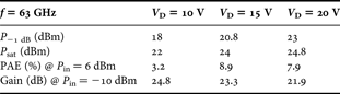
Furthermore, the impact of the drain voltage on the LS performance of the MMIC was investigated. Figure 12 shows the power gain, the output power and the PAE of the dual-gate HEMT MMIC for the drain voltages of 10, 15, and 20 V for a frequency of 63 GHz. The maximum power gain is measured for the drain bias of 10 V. For an input power of −10 dBm, a power gain of 24.8 dB was determined by measurements. Due to the relative low bias voltage for the dual-gate device, the power amplifier shows even for small input power levels (<0 dB) a high gain compression. A saturated output power of only 22 dBm (0.44 W/mm) and a maximum of about 3.4% PAE were measured for this drain bias. A higher saturated output power, P −1 dB-compression-point, and PAE can be achieved by applying a drain bias of 15 V. Within a slight decrease in the maximum power gain about 1.3 dB, a saturated output power of 24 dBm (0.7 W/mm) and a linear compression point of 20.8 dBm were measured for the power amplifier MMIC. The maximum PAE of 8.9% was determined for an input power of 6 dBm at this bias point. Further investigations showed that the LS characteristics, especially the linearity of the dual-stage power amplifier MMIC, can be further improved by the increase in drain biasing up to V D = 20 V. A very high P −1 dB- compression-point of 23 dBm was measured at 63 GHz. The saturated output power for this bias was increased to 24.8 dBm (300 mW or 0.84 W/mm). A summary of the LS characteristics of the power amplifier MMIC is given in Table 1. Further research is required to find the maximum drain voltage with respect to the reliability of the dual-gate device which holds the promise to increase the CS operation bias of 10–15 V by a factor up to 2 limited by thermal constraints only.

Fig. 12. Measured LS performance of the PA MMIC for different drain bias voltages at 63 GHz.
Table 1. LS performance of the PA MMIC for different drain bias voltages.
V. CONCLUSIONS
In this work, a dual-stage power amplifier with high gain and high output power was demonstrated by using a 100 nm AlGaN/GaN dual-gate HEMT technology. For the design of the power amplifier, a passive library and an LS model based on a state-space approach were extracted for the dual-gate HEMT. Using only two transistors in parallel for the second amplifier stage, maximum output power levels of 23.5 dBm (0.62 W/mm) for a drain voltage of 15 V at 60 GHz, and 24.8 dBm (0.84 W/mm) at 63 GHz for 20 V bias were achieved. Compared to GaAs- and InP-HEMT technologies, these results indicate that dual-gate GaN HEMTs have a great potential for increasing the bias voltage to increase power density for the mm-wave applications with high gain per stage. A maximum available gain level greater than 10 dB per stage was measured up to 100 GHz for a single GaN dual-gate HEMT which is well suited to amplifier designs at this frequency [Reference Quay9].
ACKNOWLEDGEMENTS
The authors acknowledge the continuous support of the Federal Ministry of Defense (BMVg), Bonn, the Federal Office of Defense Technology and Procurement (BWB), Koblenz, and the Bundeswehr Technical Center for Information Technology and Electronics (WTD 81), Greding.
 D. Schwantuschke was born in Koblenz, Germany, in 1984. He received the Dipl.-Ing. degree in electrical engineering and information technology from the Karlsruhe Institute of Technology (KIT), Karlsruhe, Germany, in 2010. Since 2011, he has been with the Fraunhofer Institute for Applied Solid-State Physics (IAF) in Freiburg, Germany, where he is currently working towards his doctoral degree. His research interests include the modeling of AlGaN/GaN HEMTs and the design of power amplifiers for mm-wave applications.
 C. Haupt received the Dipl.-Ing. degree in electrical engineering, with emphasis on microelectronics, from Technical University Ilmenau, Germany, in 2006. After graduation he begun working on his Ph.D. degree in the nanotechnology group at the Technical University Ilmenau in the field of GaN HFET process technology and electron beam lithography for nanostructuring. Since 2008, he is with Fraunhofer Institute of Applied Solid-State Physics where he has continued and working towards the Ph.D. degree, which he received in 2011 from the University of Freiburg, Germany. His major field of research is the process technology for GaN HFET millimeter-wave devices and nano-scaled electron beam lithography.
 R. Kiefer received his Dipl. Phys. degree in physics from the University of Freiburg, in 1979. He joined the Fraunhofer Institute of Applied Solid State Physics (IAF) in 1980 starting work on liquid crystal displays. For work on this topic he received a Ph.D. degree in physics in 1984 from the University of Freiburg. From 1984 to 1991, he investigated electro-optic effects in ferroelectric, liquid crystalline polymeric materials for optical storage applications. Afterwards, he focused his work on studying a new switching effect of nematic liquid crystals to improve the viewing angle characteristics of thin film addressed liquid crystal displays (TFT-LCD). For this work, he received an SID Award in 1998. In 1994, he moved to the field of III–V optoelectronic semiconductor technology. He managed different technology projects developing processes for fabrication and laser facet deposition of InP-based high-speed laser and GaAs as well as GaSb-based high-power laser. From 2000, his work has been focused on the development of GaN semiconductor technology for MMICs.
 P. Brückner received his Diplom-Ingenieur degree in electrical engineering from Ulm University, Ulm, in 2004. Afterwards, he joined the Institute of Optoelectronics, Ulm University, Ulm, Germany, as a Member of Scientific Staff working towards the Doktor-Ingenieur degree in the field of GaN-Epitaxy and freestanding GaN-Substrates. He received his Ph.D. in 2008. From 2008 to 2010, he was a development engineer for GaN HEMT technologies at United Monolithic Semiconductors in Ulm. He joined the Fraunhofer Institute for Applied Solid-State Physics in 2011 and is currently involved in the development of GaN HEMT technologies.
 M. Seelmann-Eggebert received his Diploma and Ph.D. degree in physics from the University of Tübingen in 1980 and 1986, respectively. From 1980 to 1996 he was involved in R&D related to infrared detectors based on HgCdTe and applied research in the field of electrochemistry and surface physics. From 1990 to 1991, he was a visiting scientist at Stanford University. From 1997 to 2000 he was engaged in the growth of CVD diamond. Since 2001 he has been a member of the department of high-frequency electronics of the IAF in Freiburg, Germany, and is in charge of the development of linear and non-linear compact models for III–V devices.
 A. Tessmann received the Dipl.-Ing. degree in electrical engineering from the University of Karlsruhe, Germany, in 1997 and the Dr.-Ing. degree in electrical engineering from the University of Karlsruhe, Germany, in 2006. In 1997, he joined the High Frequency Devices and Circuits Department, Fraunhofer Institute for Applied Solid State Physics (IAF), Freiburg, Germany, where he is involved in the development of monolithically integrated circuits and subsystems for high-resolution imaging systems. His main research areas are the design and packaging of millimeter-wave and submillimeter-wave ICs using high electron mobility transistors on GaAs, GaN and InP as well as circuit simulation and linear and nonlinear device modeling. He is currently the Group Leader of the millimeter-wave packaging and sub-system group at the Fraunhofer IAF.
 M. Mikulla received his diploma degree in electrical engineering from the Technical University of Braunschweig, Germany, in 1989 and a Ph.D. degree from the University of Ulm, Germany, in 1994. From 1994 he has been with Fraunhofer IAF in Freiburg, Germany, working on both high-power semiconductor lasers and GaN-based high-power transistors and MMICs. He has authored and has published over 100 conference/journal papers. From 2002, he has been the head of the III/V-Technology department of the institute and is also in charge of the GaN RF Power Electronics business unit.
 I. Kallfass received the Dipl.-Ing. degree in Electrical Engineering from University of Stuttgart in 2000, and the Dr.-Ing. degree from University of Ulm in 2005. In 2001, he worked as a visiting researcher at the National University of Ireland, Dublin. In 2002, he joined the department of Electron Devices and Circuits of University of Ulm as a teaching and research assistant. In 2005, he joined the Fraunhofer Institute for Applied Solid-State Physics with a focus on nonlinear millimeter-wave-integrated circuit design. Since June 2009, he has been a professor at the Karlsruhe Institute of Technology in the field of high-speed integrated circuits.
 R. Quay received the Diploma degree in physics from Rheinisch-Westfälische Technische Hochschule (RWTH) Aachen, Germany, in 1997, and a second Diplom in economics in 2003. He received his doctoral degree in technical sciences (with honors) from the Technische Universität Wien, Vienna, Austria. In 2009, he received the venia legendi (habilitation) in microelectronics, again from the Technische Universität Wien. He is currently a research engineer with the Fraunhofer Institute of Applied Solid-State Physics, Freiburg, Germany, heading the RF-devices and characterization group.


