


Introduction
Phase shifters (PSs) are widely used in the modern wireless communication and phased array systems [Reference Eldek1–Reference Lyu, Zhu and Cheng16]. In [Reference Pu, Zheng, Liu, Li and Long3–Reference Lyu, Zhu and Cheng16], several PSs with different techniques have been proposed, such as PSs based on coupled lines [Reference Pu, Zheng, Liu, Li and Long3–Reference Lyu, Zhu and Cheng7], PSs using loaded transmission lines or stubs [Reference Zheng, Chan and Man8–Reference Yu, Sun, Jing and Zhu10], PS based on the MEMS technology [Reference Llamas, Girbau, Ribo, Pradell, Giacomozzi and Colpo11], wideband PS using transversal signal-interference technique [Reference Zhu and Guo12], and PSs designed with synthesis methods [Reference Lyu, Zhu, Wu and Cheng13–Reference Lyu, Zhu and Cheng16]. For application in the multilayered microwave-integrated circuits, the components with the feature of microstrip-to-microstrip (MS-to-MS) vertical transition (VT) are always necessary [Reference Guo, Zhu, Wang and Wu17–Reference Yang, Zhu, Choi, Tam, Zhang and Wang19]. Therefore, PSs with the functionality of MS-to-MS VT are more attractive when used in the multilayered circuits and systems.
This paper proposes a high selectivity wideband 180° PS with the functionality of MS-to-MS VT in a two-layered structure. Compared with previously reported wideband 180° PSs, the proposed design shows wider bandwidth, higher selectivity, and an additional functionality of MS-to-MS VT. Based on the even/odd-mode circuit analysis theory, the simplified circuit models of even/odd-mode circuit can be obtained and a systematic design method of high filtering selectivity response is presented. To confirm the design method and performance of the proposed high selectivity wideband 180° PS, a practical PS operating at 3 GHz is simulated and measured.
Analysis of the PS
The structure of the proposed wideband 180° PS consisting of main and reference branches is shown in Figs 1(a)–1(c), which consists of two-layered substrate and three metal layers. Four λ/4 (λ is the wavelength) microstrip lines (MLs) and two ML stepped-impedance resonators (SIRs) are placed at the top and bottom layers, respectively, whereas five λ/4 slotlines (SLs) are etched on the common ground layer. To realize the high-impedance SLs at the two sides of the structure and decrease the radiation losses, four shunt-connected low-impedance SLs with the width of ws 1 are used to replace two short-circuited high-impedance SLs [Reference Yang, Zhu, Zhang, Wang, Choi, Tam and Gómez-García20]. The MLs at the top and bottom layers share the same physical dimensions. The difference between reference and main branches is only the direction of ML feedlines at the bottom layer.

Fig. 1. Structure of the proposed PS: (a) 3D layout of main branch, (b) top view of main branch, and (c) top view of reference branch.
For better understanding of phase shifting mechanism in the proposed PS, the evolution of E-field in the reference and main branches is depicted in Fig. 2. In Fig. 2, the signals of reference and main branches are fed from port 1 in the same orientation and guided to port 2 in the opposite orientations. According to the cross-view of electrical field distribution shown in Figs 2(a) and 2(b), the input E-field is converted from the −y direction to the +x direction in the ML to SL transition and propagates as SL waves until SL to ML transition. In the SL to ML transition, the E-field of main (reference) branch is converted from the +x direction to the –y (+y) direction. Thus, the E-fields at the outputs of reference and main branches propagate in the opposite direction, which amounts to 180° inserted phase. Hence, the feature of frequency independent 180° PS can be obtained by changing the coupled orientation of ML feedlines in the SL to ML transition.

Fig. 2. Evolution of E-field: (a) main branch and (b) reference branch (cyan dotted line: signal propagation path; black solid line: E-field distribution).
The transmission-line model of the proposed wideband PS is shown in Fig. 3(a) and the four shunt-connected SLs are replaced with two SLs with the impedance of Zs 1. The electrical length of the transmission-line section is assumed to be θ (= 90° at the center frequency f 0) and two pairs of impedance transformers with turns ratios of N 1 and N 2 are utilized in this design to equal to discontinuity of MLs and SLs [Reference Yang, Zhu, Choi, Tam, Zhang and Wang18].

Fig. 3. (a) Transmission-line model of the proposed PS, (b) odd-mode circuit model, and (c) even-mode circuit model.
By absorbing the transformers and normalizing characteristic impedances in Fig. 3(a), even-mode and odd-mode equivalent circuits can be obtained as shown in Figs 3(b) and 3(c), respectively. The relationships between the characteristic impedances of Figs 3(a), 3(b), and 3(c) are shown in Figs 3(b) and 3(c). The odd-mode input impedance can be expressed as

where


Similarly, the odd-mode input impedance can be obtained as

where


According to (1)–(7), the S-parameters of the proposed filter can be obtained as [Reference Zhu, Sun and Li21]


By calculating S 21 = 0, the four transmission zeros (TZs) in the stopband at the frequency range from 0 to 2f 0 can be obtained as follows:

Based on (9), the positions of the two TZs ftz 2 and ftz 4 can be controlled by tuning the ratio z 3/z 4, which is also the impedance ratio of SIR.
According to (8), the characteristic function F can be formulated as [Reference Zhu, Sun and Li21]

Figure 4(a) shows the ideal magnitude of S-parameters for the proposed PS with a quasi-elliptic equal-ripple response. In Fig. 4(a), the two TZs generated by the SIRs are ftz 2 and ftz 4, the lower cutoff frequency is fc, and RL is the return loss. The equal-ripple fractional bandwidth (FBW) can be defined as FBW = 2(f 0 – fc)/f 0.
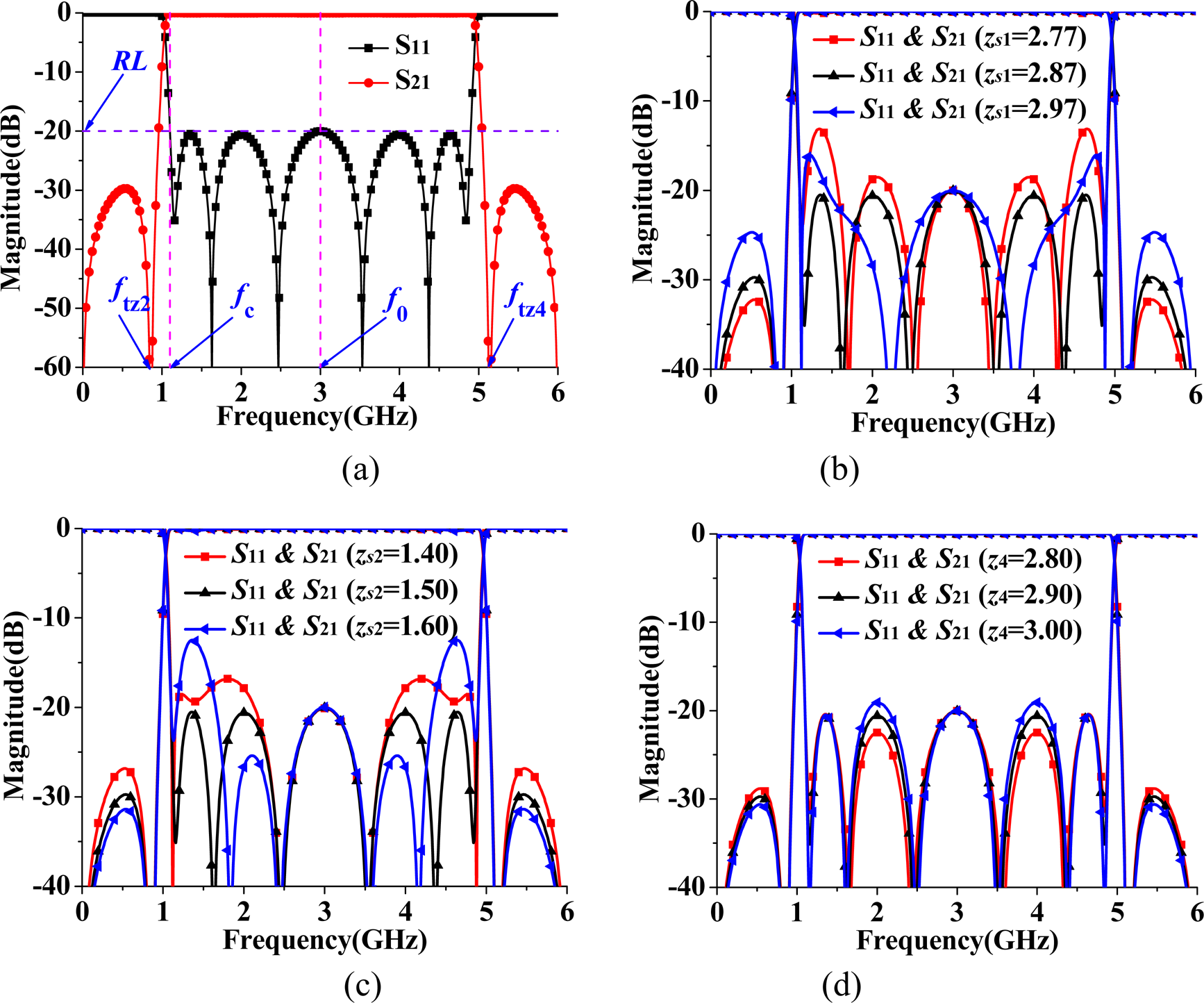
Fig. 4. (a) Ideal S-parameters of the proposed PS, (b) S-parameters with the variable zs 1 when zs 2 = 1.50 and z 4 = 2.90, (c) S-parameters with the variable zs 2 when zs 1 = 2.87 and z 4 = 2.90, and (d) S-parameters with the variable z 4 when zs 1 = 2.87 and zs 2 = 1.50.
In order to design this quasi-elliptic equal-ripple response with desired ripple FBW and RL, the following condition should be satisfied:

where

With (11), the RL at f 0 and fc can be fixed. According to (11), it can be found that:


where


By simplifying (13) and (14) with (15), the following formula can be obtained:


With given RL, FBW, ftz 2 (ftz 4), zs 1, zs 2, and z 4, the values of z 1, z 2, and z 3 can be calculated with (9), (16), and (17). For example, when f 0 = 3 GHz, FBW = 127%, and ftz 2 = 0.86 GHz, the responses of S-parameters with the variable zs 1, zs 2, and z 4 are shown in Figs 4(b), 4(c), and 4(d). The list of calculated values of z 1 and z 2 with the variable zs 1, zs 2, and z 4 in Figs 4(b), 4(c), and 4(d) are shown in Table 1. By tuning the values of zs 1, zs 2, and z 4, the desirable responses can be obtained.
Table 1. List of variables used in Fig. 4

Based on the above analysis, the values of impedance can be obtained from predetermined f 0, FBW, RL, and TZ ftz 2 (ftz 4). The design procedure for determinant of designed parameters can be given as follows:
(1) Calculate the values of θc, ε, and z 3/z 4 from predetermined f 0, FBW, RL, TZ ftz 2 (ftz 4) with (9) and (12).
(2) Based on the selected zs 1, zs 2, and z 4, the values of z 1, z 2, and z 3 can be calculated with θc, ε, and z 3/z 4 obtained in step (1) and (16)–(17).
(3) Obtain the S-parameters from the calculated values of z 1, z 2, z 3, and selected zs 1, zs 2, and z 4 in step (2) with (1)–(8).
(4) Tune the values of zs 1, zs 2, and z 4 and repeat steps (2) and (3) until desirable responses are obtained.
Experimental verification
A practical high selectivity wideband 180° PS operating at 3 GHz with FBW of 127% is designed on a two-layer Arlon AD300C substrate with a permittivity of 2.97 and a thickness of 0.762 mm in each layer. The electric parameters are listed as: N 1 = 1.06, N 2 = 1.08, Z1 = 112.00 Ω, Z 2 = 58.25 Ω, Z 3 = 30.17 Ω, Z 4 = 129.05 Ω, Zs 1 = 123.03 Ω, Zs 2 = 64.30 Ω, and Z 0 = 50.00 Ω. The photograph of the proposed wideband 180° PS is shown in Fig. 5. The dimension of the whole circuit is 0.51λg × 0.50λg × 2, where λg is the guided wavelength at f 0.

Fig. 5. The photograph of the fabricated circuit: (a) top view and (b) bottom view.
The fabricated PS is simulated by the high-frequency structure simulator and measured by the two-port vector network analyzer of Keysight N5244A. The simulated and measured results are plotted in Fig. 6. The measured insertion loss (IL) is 0.99 dB at 3 GHz. The measured bandwidth is 120% from 1.20 to 4.80 GHz for RL higher than 19 dB and phase difference of ±2.5°. Performance comparison between this paper and the-state-of-the-art PS is shown in Table 2. As it can be seen, the designed wideband 180° PS performs well in wider bandwidth, higher selectivity, and an additional functionality of MS-to-MS VT.

Fig. 6. Simulated and measured results: (a) S-parameters and (b) phase difference (Ide: ideal response; Sim: simulated result; Ref: measured result of reference branch; Main: measured result of main branch; optimized dimensions (mm) are summarized as follows: w 0 = 2.30, w 1 = 0.16, w 2 = 1.51, w 3 = 3.95, w 4 = 0.11, ws 1 = 0.56, ws 2 = 0.22, l 1 = 16.38, l 2 = 15.02, l 3 = 16.19, l 4 = 14.36, ls 1 = 19.02, ls 2 = 20.63, lvia = 1.50 and rvia = 0.50).
Table 2. Performance comparison with previous wideband PSs

Layers: number of substrate layers; RC: rectangle coefficient (RC = BW20 dB/BW3 dB, where BW20 dB is the 20-dB attenuation bandwidth of S 21 and BW3 dB is the 3-dB attenuation bandwidth of S 21).
Conclusion
In this paper, a high selectivity wideband 180° PS with the functionality of MS-to-MS VT is proposed. With the hybrid microstrip/SL structure, a frequency independent 180° PS can be obtained. Two TZs created by the SIRs are introduced to improve the skirt selectivity of the PS. It can be believed that this high selectivity wideband 180° PS can be used in the wideband radio frequency and microwave systems, which can achieve better performance in the channel selectivity and vertical interconnection.
Acknowledgement
The work was supported in part by the National Natural Science Foundation of China under Grant 61771094 and in part by Sichuan Science and Technology Program under Grant 2019JDRC0008.
 Yu Zhu was born in Anhui, China in 1992. He received his bachelor of engineering degree in electrical information engineering from Southeast University Chengxian College in 2014, and now he is pursuing Ph.D. in electronics science and technology in the University of Electronic Science and Technology of China (UESTC). His current research interests include microwave and RF passive components design.
 Kaijun Song (M’09–SM’12) received his M.S. degree in radio physics and his Ph.D. degree in electromagnetic field and microwave technology from the University of Electronic Science and Technology of China (UESTC), Chengdu, China, in 2005 and 2007, respectively. Since 2007, he has been with the EHF Key Laboratory of Science, UESTC, where he is currently a full Professor. From 2007 to 2008, he was a postdoctoral research fellow with the Montana Tech of the University of Montana, Butte, USA. From 2008 to 2010, he was a research fellow with the State Key Laboratory of Millimeter Waves of China, Department of Electronic Engineering, City University of Hong Kong. He has published more than 180 internationally refereed journal papers. His current research fields include microwave and millimeter-wave/THz power-combining technology; UWB circuits and technologies; microwave/millimeter-wave devices, circuits and systems; and microwave remote-sensing technologies.
 Yong Fan received his B.E. degree from the Nanjing University of Science and Technology, Nanjing, Jiangsu, China, in 1985, and his M.S. degree from the University of Electronic Science and Technology of China, Chengdu, Sichuan, China, in 1992. He is a senior Member of Chinese Institute of Electronics. From 1985 to 1989, he was interested in microwave-integrated circuits. Since 1989, his research interests include millimeter-wave communication, electromagnetic theory, millimeter-wave technology, and millimeter-wave systems. He has authored or coauthored over 90 papers, 30 of which are searched by SCI and EI.


