Introduction
Multi-band wireless systems have attracted much attention, because of their abilities to work at various standards [Reference Mohammadi and Ghannouchi1, Reference Keshavarz, Mohammadi and Abdipour2]. There are many applications for multi-band systems such as long-term evolution, global system for mobile communications, and wireless local area network [Reference Mohammadi and Ghannouchi1]. Accordingly, the demand for an efficient design method to realize multi-band amplifiers is very high. In this regard, dual-band amplifiers have been proposed by using the active feedback circuit technique [Reference Yamamoto3] and switches [Reference Fukuda, Okazaki, Hirota and Yamao4]. Recently, a new technique to design the dual-band circuits and systems has been devised by introducing the metamaterial transmission lines (MTM TL). The MTM TLs have special characteristics such as negative refractive index and nonlinear phase constant that can be used to achieve the various frequency responses [Reference Caloz and Itoh5]. The composite right/left handed (CRLH) TL is the most famous structure of the MTM, which is widely used in the microwave and RF circuits [Reference Hu6, Reference Caloz and Itoh7]. Several dual-band distributed amplifiers (DBDAs) using the CRLH TL were reported in 2006 [Reference Mata-Contreras, Martin-Guerrero and Camacho-Penalosa8, Reference Mata-Contreras, Martin-Guerrero and Camacho-Penalosa9]. Although this kind of DBDAs has two interesting frequency bands, its power gains are very low [Reference Mata-Contreras, Martin-Guerrero and Camacho-Penalosa8, Reference Mata-Contreras, Martin-Guerrero and Camacho-Penalosa9], which is similar to the conventional DAs. To improve the distributed amplifier (DA) gain, some methods such as cascaded gain cells [Reference Arbabian and Niknejad10–Reference Amrani, Trabelsi, Youhami and Aksas12] and negative capacitor [Reference Alavi, Ghadirian and Chabok13] have been introduced. However, all published multi-band DAs have low power gains [Reference Keshavarz, Mohammadi and Abdipour2, Reference Mata-Contreras, Martin-Guerrero and Camacho-Penalosa8, Reference Mata-Contreras, Martin-Guerrero and Camacho-Penalosa9].
In this work, a new technique to overcome the drawback of low power gain of the DBDAs is introduced. In the proposed technique, a detailed analysis for the wave attenuation coefficients of the conventional DBDAs is first provided. Then, a new unit-cell to decrease the attenuation coefficients, at a desired band is introduced. This leads to a higher power gain for the modified DBDA. It should be noted that although the new CRLH unit-cell can only increase the power gain at the forward band, in addition, by using the obtained analysis, the DBDA power gain can be increased at the other bands by another unit-cell, and a true design. To validate the results, a pHEMT DA based on the CRLH TLs is manufactured and measured. The proposed circuit exhibits a reverse power gain of 28.5 ± 1.5 dB with 2 GHz bandwidth and a forward power gain of 28.5 ± 1.2 dB with 2.5 GHz bandwidth. Furthermore, the simulation results show that the forward power gain of the DBDA is increased about 3 dB, using the introduced CRLH TL. The paper is organized as follows: The DBDA operation mechanism is given in the section “Analysis of DAs”. In the next section, the design procedure of the proposed DBDA is illustrated. In the section “Analysis of attenuation coefficient”, the theoretical analysis of the attenuation coefficient is given, and the simulation and measurement results are presented in the section “Simulation and measurement results”. Finally, concluding remarks are given in the section “Conclusion”.
Analysis of DAs
Conventional DAs
With reference to the equivalent circuit shown in Fig. 1, a classic DA consists of the cascading active devices and TLs. The forward (G fwd) and reverse (G rev) power gains of the DAs are defined as (1) and (2), respectively, [Reference Aitchison14–Reference Mori and Itoh16].
 $$G_{\,fwd} = \displaystyle{{P_{\,fwd}} \over {P_{in}}} = \displaystyle{{g_m^2 z_{0g}z_{0d}} \over 4}\left( {\displaystyle{{\sin \displaystyle{n \over 2}(\beta _g - \beta _d)} \over {\sin \displaystyle{1 \over 2}(\beta _g - \beta _d)}}} \right)^2,$$
 $$G_{rev} = \displaystyle{{P_{rev}} \over {P_{in}}} = \displaystyle{{g_m^2 z_{0g}z_{0d}} \over 4}\left( {\displaystyle{{\sin \displaystyle{n \over 2}(\beta _g + \beta _d)} \over {\sin \displaystyle{1 \over 2}(\beta _g + \beta _d)}}} \right)^2,$$
where Z 0g and Z 0d are the characteristic impedances of gate and drain lines, respectively, g m is the transconductance, β g and β d are the phase constants of the gate and drain lines, respectively, and “n” indicates the number of gain cells. It should be noted that these relations are obtained when the transistors are unilateral. Equation (1) shows that, the forward power gain (G fwd) becomes frequency-independent when β d = β g. Whereas, according to (2), the reverse power gain (G rev) is frequency-independent when β d = −β g. In the conventional DAs, gate and drain TLs are right-handed (RH) (shown in Fig. 2(a)), which the phase constant of this TL, is given by (3).
 $$\beta _{RH} = \omega \sqrt {L_g C_g} .$$
From (3), β is always positive and therefore, only the forward power gain (S 41) of the conventional DA is usable. This condition can be changed by replacing the RH TL with the CRLH TL.

Fig. 1. Conventional distributed amplifier.

Fig. 2. (a) RH and (b) CRLH unit cell.
CRLH TL
Figure 2(b) shows the equivalent circuit of a CRLH TL. The CRLH TL consists of a series LC resonator (Z d) in the horizontal branch and a parallel LC resonator (Y d) in the vertical branch. The phase constant of the CRLH TL can be obtained as follows [Reference Lai, Itoh and Caloz17]:
 $$\beta = s(\omega )\sqrt {\, \, \left( {\omega C_R - \displaystyle{1 \over {\omega L_L}}} \right) \times \left( {\omega L_R - \displaystyle{1 \over {\omega C_L}}} \right)} ,$$
where s(ω) is the following:
 $$s(\omega ) = \left\{ \matrix{ - 1\quad {\rm if}\quad \omega \le \min (\omega _{se} = 1/\sqrt {C_RL_L} {\mkern 1mu}, \omega _{sh} \hfill \cr \quad = 1/\sqrt {C_LL_R} {\mkern 1mu} \;)\quad {\rm LH}{\mkern 1mu} {\rm range} \hfill \cr + 1\quad {\rm if}\quad \omega \ge \max {\mkern 1mu} (\omega _{se} = 1/\sqrt {C_RL_L} {\mkern 1mu}, \omega _{sh} \hfill \cr \quad = 1/\sqrt {C_LL_R} {\mkern 1mu} \;)\quad {\rm RH}{\mkern 1mu} {\rm range}. \hfill} \right.$$
DBDA with CRLH TL
Equation (4) shows that unlike the RH TLs, the CRLH TLs can have β < 0. Therefore, by replacing the RH TL with the CRLH TL in a DA, the situations of −β d = β g and β d = β g could be achieved at two various frequencies, respectively [Reference Mata-Contreras, Martin-Guerrero and Camacho-Penalosa9]. As a result, both forward and reverse gains could be frequency-independent.
Design of the DBDA
The main structure of the proposed DBDA is illustrated in Fig. 3. Port 1 and Port 2 are the input and isolated ports, respectively, and Port 3 and Port 4 are the output ports. This structure amplifies the input signals at two various frequency bands, with center frequencies of f 1 and f 2 and then extracts them from Ports 3 and 4, respectively.

Fig. 3. Schematic of the proposed DBDA.
Design of the TLs
As shown in Fig. (3), the gate and drain lines of the proposed DBDA are provided by the RH and CRLH TLs, respectively. There are two reasons for these choices: First, by selecting the CRLH TL as the gate line, it has the significant effects and distortions on the return loss (S 11), therefore, the RH TL is selected as the gate line. Second, by increasing the number of gain cells (longer gate TL), the wave attenuation of the gate line increases and finally, it can surpass the amplification. Thus, the number of gain cells is limited by the attenuation of the gate line. As a result, since the RH TL has the lower attenuation than the artificial TL [Reference Caloz and Itoh5], it should be selected as the gate line.
To design the TLs, first, the desired frequency ranges for the forward (f 2) and reverse (f 1) power gains should be determined.
There are two points to note about f 1 and f 2 frequencies:
(i) In fact, by a suitable approximation, f 1 and f 2 are the center frequencies of the reverse and forward bands and therefore these frequencies must be carefully selected. However, parasitic elements and transistor model errors can change this issue.
(ii) It should be noted that by increasing the value of f 2 than f 1, the wider frequency bands for the DBDA are obtained.
But the proposed DBDA is designed by using ATF36-163 HEMT transistor, that its gain decreases after 10 GHz, severely. Then f 1 = 4 GHz and f 2 = 8 GHz are selected. It is clear that by using the transistors with higher f t, achieving a higher f 2 and accordingly a wider bandwidth is possible.
From (5), the RH TLs are fully determined by their matching conditions and phase specifications, at a single operating frequency [Reference Caloz and Itoh5].
 $$\left\{ {\matrix{ {C_g = \beta _1/\omega _1Z_{0C}}\cr{L_g = Z_{0C}^2 C_g}\cr } } \right.{\rm},$$
where Z 0C is the characteristic impendence, and is selected equal to the port impedance (50 Ω), to achieve a wide band matching [Reference Caloz and Itoh5]. In addition, the phase constant of the RH TL is a linear function of frequency (Eq. (5)). Therefore, the whole dispersion curve is determined by having the value of β at a specified frequency. On the other hand, unlike the RH TLs, CRLH TLs have four elements in their circuit models (instead of two), and their dispersion curves are nonlinear. Therefore, designers have a greater degree of freedom. Hence, the design procedure is started by designing a RH TL as the gate line. In this regard, an arbitrary value for β g(f 1) should be selected. In this paper, it is assumed that β g(4 GHz) = 0.65 (rad/m). From (3), β g equals 1.3 (rad/m) at 8 GHz frequency. As a result, to achieve the DBDA, a CRLH TL should be designed as the drain line, such that the following conditions are satisfied:
 $$\beta _d(4\, {\rm GHz}) =- 0.65({\rm rad}/{\rm m})\quad {\rm and}\quad \beta _d(8\, {\rm GHz}) = 1.3\, ({\rm rad}/{\rm m}).$$
The components values of the CRLH unit-cell can be obtained as below [Reference Caloz and Itoh5]:
 $$\left\{ \matrix{C_R = (\beta _1\omega _1 - \beta _2\omega _2)/(Z_{0C}(\omega _1^2 - \omega _2^2 ))\; \hfill \cr C_L = 1/\left( {\omega _1^2 - \displaystyle{{\beta _1\omega _1} \over {Z_{0C}C_R}}} \right)Z_{0C}^2 C_R\; \hfill \cr L_R = Z_{0C}^2 C_R \hfill \cr L_L = Z_{0C}^2 C_L, \hfill} \right.$$
where Z 0C is the characteristic impedance, and is selected equal to the port impedance (50Ω) to achieve a wide band matching [Reference Caloz and Itoh5]. Table 1 shows the calculated element values of TLs, using (5)–(7). According to the given values in Table 1, the dispersion curves of the gate and drain lines are plotted in Fig. 4. As shown in the figure, the phase constants of the gate and drain TLs are the same at two frequencies of 4 GHz and 8 GHz. Therefore, the design procedure of TLs to achieve a DBDA is completed.

Fig. 4. Dispersion curves of the designed RH (dashed line) and CRLH TLs (solid line).
Table 1. Lumped elements for the TLs

Overall structure of the proposed DBDA
As mentioned previously, DAs have a broad bandwidth while their gains are low, due to the additive gain mechanism [Reference Mohammadi and Ghannouchi1]. In recent years, to solve the low gain problem of DAs, many topologies have been reported, such as cascaded single stage DAs (CSSDA) [Reference Mohammadi and Ghannouchi1] and matrix DAs [Reference Moez and Elmasry18], which their gain mechanisms are multiplicative. Therefore, to realize a high-gain DBDA, the proposed structure is designed based on the multiplicative gain mechanism, as the first step. As shown in Fig. 3, the gain cell is realized by two cascaded common-source transistors. Simulation of the designed DBDA is performed using the ADS simulator. The results are shown in Fig. 5, and the proposed DBDA achieves a forward power gain (S 41) of 24.5 ± 1 dB, and a reverse power gain (S 31) of 27.5 ± 1. Although the designed structure has a high power gain compared with the other reported multi-band DAs [Reference Keshavarz, Mohammadi and Abdipour2, Reference Mata-Contreras, Martin-Guerrero and Camacho-Penalosa8, Reference Mata-Contreras, Martin-Guerrero and Camacho-Penalosa9], the forward power gain is about 3 dB lower than the reverse power gain. This issue can be related to the increase of the parasitic effects with frequency. In the section “Analysis of attenuation coefficient”, to reduce the power gain difference between S 31 and S 41 of the introduced DBDA and to increase the power gain at the forward band, a new method is presented.

Fig. 5. S-Parameters of the DBDA with the conventional unit-cells.
Analysis of attenuation coefficient
Preliminary
In the general case, with the bilateral (S 12T ≠ 0) transistors, the wave propagation constants of drain and gate lines have a positive real part, even when transmission lines are lossless [Reference Nikandish and Medi19]. In this work, by decreasing the wave attenuation coefficient in the proposed DBDA, its power gain at the forward band is enhanced. To provide insight, the attenuation coefficients of the conventional DBDAs were first calculated and then compared with the proposed DBDA. The equivalent circuit of a small segment of a DA is shown in Fig. 6. Using the voltage and current equations in the drain and gate lines, the voltages in the gate and drain lines can be described by the following system of the linear partial differential equations [Reference Nikandish and Medi19]:
 $$\displaystyle{{\partial ^2} \over {\partial x^2}}\left[ {\matrix{{v_g} \cr{v_d} \cr } } \right] = \left[ {\matrix{{A_{11}} & {A_{12}} \cr{A_{21}} & {A_{22}} \cr } } \right]\left[ {\matrix{{v_g} \cr{v_d} \cr } } \right],$$
where A 11 = z g(y g + y gd), A 12 = −z gy gd, A 21 = (g m − y gd)z d, and A 22 = z d(y d + y gd). In addition, z g, y g, z d, and y d can be determined from Fig. 2. By applying the Laplace transform on (8), a characteristic equation is derived as below [Reference Nikandish and Medi19]:
 $$({{S}^{2}}-{{A}_{11}})({{S}^{2}}-{{A}_{22}})-{{A}_{12}}{{A}_{21}}=0,$$
where “S” is the laplace frequency. It should be noted that to present a comprehensive analysis for the attenuation coefficients, the relations of this section are obtained when the transistors are bilateral. Furthermore, the voltage waves in the gate and drain lines have the general form of (10) [Reference Nikandish and Medi19].
 $$V(x)={{k}_{1}}{{e}^{-{{\gamma }_{1}}x}}+{{k}_{2}}{{e}^{{{\gamma }_{1}}x}}+{{k}_{3}}{{e}^{-{{\gamma }_{2}}x}}+{{k}_{4}}{{e}^{{{\gamma }_{2}}x}}.$$
Using (8) and (9), the propagation constants of the DA (γ 1,2) are derived as follows [Reference Nikandish and Medi19]:
 $$\gamma _{1,2} = \alpha _{1,2} + j\beta _{1,2} = \sqrt {\displaystyle{{A \pm \sqrt {B + 4C)} } \over 2}},$$
where A = A 11 + A 22, B = (A 11 − A 22)2, and C = A 12A 21.
 $$\eqalign{ A &= z_g(y_g + y_{gd}) + z_d(y_d + y_{gd}) \cr & = (\,j^2\omega ^2L_gC_g^{\prime}) + (\,j\omega L_r + \displaystyle{1 \over {\,j\omega C_l}})\left( {\,j\omega C_{gr} + \displaystyle{1 \over {\,j\omega L_l}}} \right) \cr B & = \left( {z_g(y_g + y_{gd}) - z_d(y_d + y_{gd})} \right)^2 \cr & = \left( {(\,j^2\omega ^2L_gC_g^{\prime} ) - \left( {\,j\omega L_r + \displaystyle{1 \over {\,j\omega C_l}}} \right)\left( {\,j\omega C_{gr} + \displaystyle{1 \over {\,j\omega L_l}}} \right)} \right)^2 \cr C & = - (g_m - j\omega C_{gd})\left( {\,j\omega L_r + \displaystyle{1 \over {\,j\omega C_l}}} \right) \cr & \times (\,j\omega C_{gd} \times j\omega L_g){\mkern 1mu} {\mkern 1mu} {\rm and}{\mkern 1mu} {\mkern 1mu} C_g^{\prime} = C_g + C_{gd}.} $$
The real parts of γ 1,2 (α 1 and α 2), are plotted in Fig. 7. As mentioned previously, the goal of the paper is to decrease the attenuation coefficients at the desired frequency band, which is shown in the rectangular area of Fig. 7. From (11), the attenuation coefficient (α) is minimized when:
 $${A \pm \Re {\rm e}\sqrt {B + 4C} \lt\; 0\;\& \left\{ {\matrix{ {(1)\, A \pm \Re {\rm e}(\sqrt {B + 4C} ) \to- \infty }\cr{(2)\quad or\quad {\rm Im}(\sqrt {B + 4C} ) \to 0}\cr } } \right. }.$$
And α is maximized when:
 $$A \pm \Re {\rm e}{\sqrt {B + 4C}} \gt \; 0\quad \& \left\{ {\matrix{ {(1)\, A \pm \Re {\rm e}(\sqrt {B + 4C} ) \to+ \infty }\cr{(2)\quad or\quad {\rm Im}(\sqrt {B + 4C} ) \to 0.}\cr } } \right.$$
 $$\left\{ {(3)\quad {\rm Im}(\sqrt {B + 4C} ) \to\;+ \infty \quad \& \;A \pm \Re {\rm e}(\sqrt {B + 4C} ) \lt 0.} \right.$$
The proof of equation (12) is given in appendix A.

Fig. 6. Equivalent circuit of a small segment of the DA.

Fig. 7. The attention coefficients of the DBDA (the elements are selected as Table 1).
Finding the corresponding frequencies to αmin
In the case where  $A\pm \Re {\rm e}(\sqrt {B+4C})\to -\infty $
Equation (12a-1) shows that the attenuation coefficient (α) is minimized when either term “A” or  $\Re {\rm e}(\sqrt {B+4C})$ goes to −∞. In the general case, A and
  $\Re {\rm e}(\sqrt {B+4C})$ are always negative and positive, respectively (as will be seen in Fig. 15), and the magnitude of A is always greater than
  $\Re {\rm e}(\sqrt {B+4C})$, which guarantees the negative sign for (
 $ A\pm \Re {\rm e}(\sqrt {B+4C})$). In other words, to find the corresponding frequencies to α min, the poles of term “A” should be calculated as follows:
 $$\eqalign{& A = z_g(y_g + y_{gd}) + z_d(y_d + y_{gd}) = (\,j^2\omega ^2L_gC_g^{\prime} ) \cr & \quad \quad + \left( {\,j\omega L_r + \displaystyle{1 \over {\,j\omega C_l}}} \right)\left( {\,j\omega C_r + \displaystyle{1 \over {\,j\omega L_l}}} \right) \cr & \quad = - \infty \Rightarrow z_dy_d = - \infty \Rightarrow \omega _{\alpha _{1,2}{\min }_1} = 0.} $$
From (13), since z g, y g, and y gd do not have any poles, poles of “A” are the same with Z d and Y d (where Z d and Y d are the horizontal branch impedance and the vertical branch admittance of the CRLH unit cell, respectively).
In the case where ${\rm Im}(\sqrt {B+4C})\to 0$
In addition, according to (12a-2), the attenuation coefficient (α) is minimized when:
 $$\eqalign{& {\rm Im}(\sqrt {B + 4C} ) \to 0\buildrel {B\,{\rm is\,purely\,real}{\mkern 1mu} } \over \rightarrow {\rm Im}(C) = 0 \cr & \quad \Rightarrow {\rm Im}\left[ { - \left( {g_m - j\omega C_{gd}} \right)\left( {\,j\omega L_r + \displaystyle{1 \over {\,j\omega C_l}}) \times (\,j^2\omega ^2C_{gd}L_g} \right)} \right] = 0 \cr & \quad \Rightarrow j\omega L_r + \displaystyle{1 \over {\,j\omega C_l}} = 0 \Rightarrow \omega _{\alpha _{1,2}{\min }_2} = \displaystyle{1 \over {\sqrt {L_rC_l} }}.} $$
Thus, in the DBDAs based on the conventional CRLH TL, α 1,2 are minimized at the zero frequency of the horizontal branch (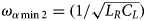 ${{\omega }_{\alpha \min 2}} = ({1}/{\sqrt {{{L}_{R}}{{C}_{L}}}})$) and pole frequencies of the horizontal and vertical branches (ω α min 1 = 0). As a result, the attenuation coefficient can be decreased at the desired frequency band, by adding a suitable pole to one of the branches (horizontal or vertical) of the CRLH. This goal is achieved by introducing a new CRLH TL.
Adding a new minimum point to α curve, in the Case $A \pm \Re {\rm e}(\sqrt {B+4C}) \to -\infty $

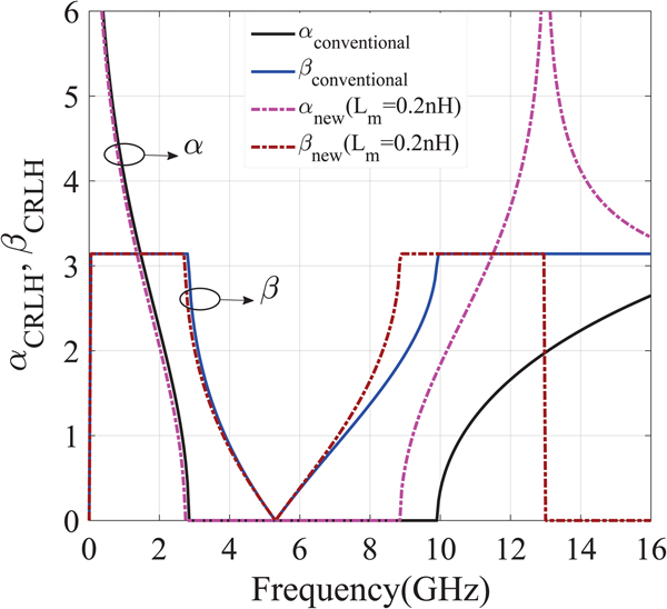
Figure 8 shows the proposed CRLH unit cell. As shown in the figure, the horizontal branch of the proposed topology is similar to the conventional CRLH TL, but in the vertical branch, a series inductor (L m) is added to the parallel LC resonator. The attenuation and phase constants of this TL, in comparison with the conventional type, are illustrated in Fig. 9. It is clear that the difference between these two TLs is noticeable, only at the RH band. Hence, it is expected that by using the introduced TL, only S 41 of the proposed DBDA is changed. From Fig. 8, the admittance of the vertical branch is equal to:
 $$Y_{d_{new}} = \displaystyle{1 \over j\omega L_m + \displaystyle{1 \over j\omega C_r + (1/j\omega L_l)}} = \displaystyle{{(\,j^2 \omega^2 L_l C_r) + 1} \over {\,j\omega (L_m (\,j^2 \omega^2 L_l C_r) + (L_m + L_l))}}.$$
According to (15), the vertical branch admittance (Y dnew) of the proposed CRLH TL has two acceptable poles in comparison with the single pole of the conventional CRLH TL. The new pole of Y dnew is obtained as below:
 $$\eqalign{& Y_{dnew} \to \infty \Rightarrow \displaystyle{{(\,j^2\omega ^2L_lC_r) + 1} \over {\,j\omega L_m(\,j^2\omega ^2L_lC_r) + j\omega L_l}} \to \infty \cr & \quad \quad \quad \quad \Rightarrow j\omega L_m(\,j^2\omega ^2L_lC_r) + j\omega L_l = 0 \to \omega _{\alpha _{1,2}\min 3} \cr & \quad = \sqrt {\displaystyle{{L_l/L_m + 1} \over {C_rL_l}}} .} $$
Figure 10 shows the attenuation coefficients for the proposed structure. As expected, using the introduced CRLH, α becomes zero at three frequencies in opposition to the conventional type, which the number of these frequencies is two. It can also be observed that the wave attenuation coefficient is severely decreased at frequencies between ω α,min 2 and ω α,min 3, leading to higher power gain for the structure. From Fig. 11, by using the proposed CRLH, the forward power gain (S 41) is increased about 3 dB and the level difference between S 31 and S 41 is removed.

Fig. 8. The proposed CRLH TL.

Fig. 9. β and α for the CRLH unit cell.

Fig. 10. The attention coefficients of the DBDA (solid lines: using the conventional CRLH TL, dotted lines: using the proposed CRLH TL, L m = 0.2 nH).
Fig. 11. S-Parameters of the proposed DBDA: using the conventional CRLH TL (solid lines: L m = 0), using the proposed CRLH TL (dashed lines: L m = 0.4 nH).
Simulation and measurement results
To validate the discussed analysis, a DBDA was designed using the ATF36163 HEMT transistor. It has been fabricated on the RO4003C substrate with the relative permittivity of 3.55, loss tangent equal to 0.0027, and thickness of 0.5 mm. The required series capacitor (C L) in the CRLH unit cell is provided by the interdigital capacitor, and the capacitance value (C L) and the inductance value (L R) (shown in Fig. 2) depend on the number and thickness of the interdigital fingers and their gap width. The output impedance of the active device is used to make the capacitance C R and inductance L L. Also, the transmission line between the active devices and the drain TL creates the inductor (L m) of the proposed CRLH TL. It should be noted that, there are limitations on the realization of TLs:
1) In the general case, since the series capacitance C L (shown in Fig. 2) is usually provided by an interdigital capacitor, designers have several technological limitations: First, the interdigital capacitor has a poor capacitance per-unit-length, especially at microwave frequencies. Secondly, the bandwidths of these structures are limited by spurious transverse resonances of the interdigital capacitor. In fact, designers to realize the capacitance higher than 1 PF (using interdigital capacitor) have many problems, due to the imposed spurious transverse resonances. Therefore, there is a minimum operating frequency to choose.
2) On the other hand, the operating frequency cannot be increased to any desired value, since to achieve that, the element values of the metamaterial unit cell should be selected as small as necessary. But this is impossible, because of the parasitic elements of the active devices (which play an important role to realize these unit cells) cannot be reduced to the extent necessary. Therefore, according to the used technology, there is a maximum frequency to choose.
The transistors were biased at V drain = 1.3 V, V source = 0 V, V gate = 0.2 V. The total drain current for transistors was 40 mA, and for DC bias, the lumped discrete capacitors (100 pF) were utilized as dc blocks in several points on the board. Figure 12 shows the photograph of the fabricated circuit, which its total chip area is 17.5 (3 cm × 5.5 cm). As shown in the figure, the proposed DBDA is composed of two main parts:
1) A CSSDA is attached to the input port which includes two cascaded transistors and an input matching circuit. There are two reasons for adding this part to the proposed structure: when the pre-amplifier is removed, the gate TL is responsible for the input matching. Furthermore, as said before, to provide a DBDA, the gate and drain TLs should be designed such that condition (6) is satisfied. As a result, there are some problems to achieve the input matching and condition (6), simultaneously. By adding the preamplifier, the isolation between the input port and the gate line is improved. Hence, easier access to the input matching at the wide bandwidth and a greater degree of freedom to design the gate line are achieved.
2) A common DA, in which the drain TL was constructed by the CRLH TL and converts the DA into the DBDA. The gain cell of this part was formed by two cascaded common-source transistors.
To provide insight, the preamplifier and the DBDA parts are simulated separately, and the results are shown in Fig. 13. As illustrated, the preamplifier has a power gain of 12.5 dB, and therefore it plays an important role in improving the power gain. Furthermore, the DBDA part by having the forward and reverse power gains of 13 dB provides a dual band amplifier.

Fig. 12. Photograph of the fabricated DBDA.

Fig. 13. The power gains of the (a) preamplifier, (b) DBDA part.
The scattering parameters of the DBDA are plotted in Fig. 14. From Fig. 14(a), the return loss (S 11) of the designed DBDA is better than 10 dB through the forward and reverse frequency bands. As shown in Fig. 14(b), the DBDA achieves 28.5 ± 1.2 dB forward gain (S 41) and 28.5 ± 1.5 dB backward gain (S 31). In addition, the 3-dB bandwidths of the forward and backward power gains are 2.5 GHz (from 5.5 to 8 GHz) and 2 GHz (from 2 to 4 GHz), respectively. The obtained bandwidth is good in comparison with the conventional DBDAs. In addition, simulated and measured results show an acceptable agreement. Some reported multi-band DAs are presented in Table 2, for comparison. It is clear that the proposed circuit has a higher power gain and wider bandwidth, than the other reported DBDAs.

Fig. 14. S-parameters of the DBDA: (a) S 11 and (b) power gains of the proposed DBDA (solid lines: full-wave simulation, dotted lines: measurement).

Fig. 15. The variation of terms “A” and  ${\rm real}(\sqrt {B+C})$ versus frequency using: (Solid lines: L m = 0, dotted lines: L m = 0.2 nH).
Table 2. Comparison of the results for multi-band DAs.

Conclusion
A high-gain dual-band DA with composite right/left-handed transmission line has been presented. By using a new CRLH TL in the DBDA, the attenuation coefficients have decreased, leading to increased S 41 for the structure, (about 3 dB at high-frequency band). The proposed method can be used to increase the power gain of the DAs or other active circuits which use the metamaterial TL. The proposed circuit exhibits 28.2 dB reverse gain with a bandwidth of 2 GHz and 28.5 dB forward gain with a bandwidth of 2.5 GHz.
Acknowledgments
The authors would like to thank Iranshahr Velayat University for help and support with measurements.
APPENDIX A
Eq. (11) can be written in a general form as follows:
 $$\gamma =\sqrt{a+jb},$$
The real and imaginary parts of (A.1) are obtained from (A.2a) and (A.2b).
 $$\Re {\rm e}(\gamma ) = \alpha= \sqrt {\sqrt {a^2 + b^2} }\times \cos \left( {0.5 \times {\tan }^{ - 1}\left( {\displaystyle{b \over a}} \right)} \right),$$
 $${\rm Im}(\gamma ) = \sqrt {\sqrt {a^2 + b^2} }\times \sin \left( {0.5 \times {\tan }^{ - 1}\left( {\displaystyle{b \over a}} \right)} \right).$$
According to (A.2a), α is minimized when
 $$\tan ^{ - 1}\left( {\displaystyle{b \over a}} \right) \to \pi\Leftrightarrow \left\{ {\matrix{ {1)\;a \to- \infty } \hfill\cr{2)\;b \to 0\quad \& \quad a \lt 0,} \hfill\cr } } \right.$$
and α is maximized when
 $$\eqalign{& \tan ^{ - 1}\left( {\displaystyle{b \over a}} \right) \to 0 \Leftrightarrow \left\{ \matrix{1)\;a \to + \infty \hfill \cr 2)\;b \to 0\quad \& \quad a \gt 0 \hfill} \right. \cr & \quad \quad \quad \quad \quad \quad \quad \big\{ {3)\;b \to + \infty \quad \& \quad a \lt 0.} }$$
By comparing (11) and (A.1), it can be concluded that:
 $$\left\{ {\matrix{ {a = \Re {\rm e}\left( {A \pm \sqrt {B + 4C} } \right)\mathrel{\mathop{\kern0pt\longrightarrow}\limits_{C{\kern 1pt} {\rm is}{\kern 1pt} {\rm complex}}^{A{\kern 1pt} {\rm and}{\kern 1pt} B{\kern 1pt} {\kern 1pt} {\rm are}{\kern 1pt} {\rm real}}} a = A \pm \Re {\rm e}\left( {\sqrt {B + 4C} } \right)} \hfill \cr {b = {\mathop{\rm Im}\nolimits} \left( {A \pm \sqrt {B + 4C} } \right)\mathrel{\mathop{\kern0pt\longrightarrow}\limits_{C{\kern 1pt} is{\kern 1pt} {\rm complex}}^{A{\kern 1pt} {\rm and}{\kern 1pt} B{\kern 1pt} {\kern 1pt} {\rm are}{\kern 1pt} {\rm real}}} b = {\mathop{\rm Im}\nolimits} \left( {\sqrt {B + 4C} } \right).} \hfill \cr } } \right.$$
Hence, (A.3a) and (A.3b) can be rewritten as follow:
 $$\alpha _{{\rm min}} \Leftrightarrow A \pm \Re {\rm e}\sqrt {B + 4C} \lt \;0\;\& \left\{ {\matrix{ {(1)\;A \pm \Re {\rm e}(\sqrt {B + 4C} ) \to - \infty } \hfill \cr {(2)\quad {\rm or}\quad {\rm Im}(\sqrt {B + 4C} ) \to 0} \hfill \cr } } \right.$$
 $$\eqalign{& \alpha _{{\rm max}} \Leftrightarrow {\mkern 1mu} {\mkern 1mu} A \pm \Re {\rm e}\sqrt {B + 4C} \gt 0\,\quad \cr & \quad \& \left\{ \matrix{(1)\;A\; \pm \Re {\rm e}(\sqrt {B + 4C} ) \to + \infty \hfill \cr (2)\quad or\quad {\rm Im}(\sqrt {B + 4C} ) \to 0, \hfill} \right.}$$
 $$\left\{ {(3)\;{\rm Im}(\sqrt {B + 4C} ) \to + \infty \, \, \& \, A \pm \Re {\rm e}(\sqrt {B + 4C} ) \lt 0.} \right.$$
These equations can be used to design the proposed CRLH TL with the minimum attenuation coefficients at an arbitrary frequency band. Note that, to simplify the analysis, “2” in (11) was removed because it has no effect on the analysis.
APPENDIX B
Finding the corresponding frequencies to αmax
In the case where $A\pm \Re {\rm e}(\sqrt {B+4C})\to +\infty \,$
Equation (A.5b) shows that the attenuation coefficients are maximized when  $A\pm \Re {\rm e}(\sqrt {B+4C})\to + \infty $. As said previously, by using the conventional CRLH,
  $A\pm \Re {\rm e}(\sqrt {B+4C})$ is always negative, but this situation is changed by using the proposed CRLH TL. As shown in Fig. 15, the terms “A” and
  $\Re {\rm e}(\sqrt {B+4C})$ are always negative and positive, respectively. Using the proposed CRLH, “A” becomes positive, which can transform
  $ A\pm \Re {\rm e}(\sqrt {B+4C})$ to a positive value, when
 $$\eqalign{& A + \Re {\rm e}(\sqrt {B + 4C} ) \gt 0{\mkern 1mu} {\mkern 1mu} \to A \gt \cr & \quad - \Re {\rm e}(\sqrt {B + 4C} ){\mkern 1mu} {\mkern 1mu} \Rightarrow {\rm Great}{\mkern 1mu} {\mkern 1mu} {\rm \;increment}{\mkern 1mu} \;{\rm of}\ \alpha _1,}$$
 $$\eqalign{& A - \Re {\rm e}(\sqrt {B + 4C} ) \gt 0{\mkern 1mu} \to A \gt \cr & \quad \Re {\rm e}(\sqrt {B + 4C} ){\mkern 1mu} {\mkern 1mu} \Rightarrow \;{\rm Great}{\mkern 1mu} {\mkern 1mu} \;{\rm increment}{\mkern 1mu} \;{\rm of}\ \alpha _2.}$$
From Fig. 15, Equation (B.1a) is satisfied at frequencies higher than ω α min 3 = 12.8 GHz, limiting the bandwidth. But (B.1b) cannot be satisfied, and α 2 did not show a peak at the pole frequency ω α min 3, as is cleared in Fig. 10.
In the case where ${\mathop{\rm Im}\nolimits} \sqrt {B + 4C} \to + \infty $
According to (A.5c), α is maximized when  ${\rm Im}\sqrt {B + 4C} \to + \infty$ and
  $ A\pm \Re {\rm e}(\sqrt {B+4C})<0$. From Fig. 15,
  $ A\pm \Re {\rm e}(\sqrt {B+4C})<0$ is satisfied at frequencies lower than ω α min 3 = 12.8 GHz. In addition, from (A.2b),
  ${\mathop{\rm Im}\nolimits} \sqrt {B_{new} + 4C}$ becomes large when sin (0.5 tan−1 (4C/B new)) approaches one; therefore:
 $${\mathop{\rm Im}\nolimits} \sqrt {B + 4C}\to+ \infty\Rightarrow \sin \left( {0.5\, {\tan }^{ - 1}\displaystyle{{4C} \over {B_{new}}}} \right) \to 1\,\Rightarrow \tan ^{ - 1}\displaystyle{{4C} \over {B_{new}}} \to \pi $$
“B new” can be obtained from (B.3):
 $$ \eqalign{B_{new} &= \left( \vphantom{\left( {\displaystyle{1 \over {\,j\omega L_m +\displaystyle{1 \over {\,j\omega C_r + (1/j\omega L_l)}}}} + j\omega C_{gd}} \right)} (\,j^2\omega ^2L_g{C}^{\prime}g) - \left( {\,j\omega L_r + \displaystyle{1 \over {\,j\omega C_l}}} \right)\right. \cr & \quad\times \left.\left( {\displaystyle{1 \over {\,j\omega L_m +\displaystyle{1 \over {\,j\omega C_r + (1/j\omega L_l)}}}} + j\omega C_{gd}} \right) \right)^2.}$$
According to (B.3) and selected element values for the designed circuit, term “B new” is a positive real value; thus, (B.2) is not satisfied and max (tan−1(4C/B new)) is equal to ±π/2, which is established when B new = 0. Finally, by equating term B new to zero, six frequencies are obtained, but only two of them are acceptable, f 1 = 4 GHz, f 2 = 7 GHz, in which α is maximized, as is shown in Fig. 10.
 $$\eqalign{ B_{new} & = 0 \Rightarrow \omega ^6(C_lC_rC_{gd}L_lL_rl_m - C_lC_r{{C}^{\prime}}_gL_lL_mL_g) \cr & \quad - \omega ^4(C_lC_rL_lL_r + C_lC_{gd}{{L}^{\prime}}_lL_r + C_rC_{gd}L_ll_m - C_l{{C}^{\prime}}_gL_g{{L}^{\prime}}_l) \cr & \quad + \omega ^2(C_lL_r + C_rL_l + C_{gd}{{L}^{\prime}}_l) - 1 = 0,}$$
where  $L_{l}^{'} = L_m + L_l$.
 Hamed shahraki received the B.Sc. degree in electrical engineering from University of Sistan and Baluchestan, Zahedan, Iran, in 2008, the M.S. degree in Electrical Engineering from Shiraz University of Technology, Shiraz, Iran, in 2012, and is currently working toward the Ph.D. degree at the Shahid Bahonar University of Kerman, Kerman, Iran. His research interests are MTM, RF/microwave circuits design. He is currently involved with microwave devices based on CRLH TL.
 Ahmad hakimi received his B.Sc. degree in Electrical Engineering from Technical College of Shahid Bahonar University of Kerman, Kerman, Iran, in 1986. Using the scholarship granted by the Ministry of Higher Education of Iran and Istanbul Technical University (ITU) in 1987, he started studying his M.Sc. and Ph.D. degrees in the Faculty of Electrical and Electronic Engineering at the ITU and received his M.Sc. and Ph.D. degrees in 1990 and 1996, respectively. His research interests include design and analysis of nonlinear RF circuits, numerical analysis and advanced engineering mathematics, analog filter design, and linear integrated circuits. He is currently with the Scientific and Industrial Research Center, Kerman, Iran, and the Department of Electrical Engineering, Shahid Bahonar University of Kerman, Kerman, Iran.
 Kambiz Afrooz received the B.Sc. degree from the Shahid Bahonar University of Kerman, Kerman, Iran, in 2005, the M.Sc. and Ph.D. degrees from the Amirkabir University of Technology (Tehran Polytechnic), Tehran, Iran, in 2007 and 2012, all in Electrical Engineering. In May 2011, he joined the CIMITEC group, University Autonoma de Barcelona (UAB), Barcelona, Spain, as a Visiting Student. He is currently an Associate Professor with the Electrical Engineering Department, Shahid Bahonar University of Kerman, Kerman, Iran. His research interests are in the areas of computer aided design of active and passive microwave devices and circuits, computational electromagnetic, modeling and simulation of high speed interconnects, metamaterial transmission lines, and substrate integrated waveguide structures. He is also the recipient of the Electrical Engineering Department Outstanding Student Award in 2007.
 Mohammad Mahdi Pezhman received the B.Sc. degree in Electrical Engineering from the Shahid Bahonar University of Kerman, Kerman, Iran, in 2012. He received the M.Sc. degree in electrical engineering at the Kerman Graduate University of Technology, Kerman, Iran, in 2014. Now, he is the Ph.D. student of Yazd University and his research interests include design of RF building blocks for ultra-wideband amplifier and composite Right/handed transmission line. The focus of his research is on design of dual-band distributed amplifier (DBDA) with high gain and low power consumption.