


Introduction
Dielectric resonator antennas (DRAs), first proposed by Long et.al. [Reference Long, McAllister and Shen1], are known for their higher radiation efficiency and bandwidth compared to microstrip patch antennas, the flexibility to excite a variety of radiating modes, compact designs, and the compatibility with standard feed schemes [Reference Petosa and Ittipiboon2]. The cylindrical shaped DRA (CDRA) is very popular, and its fundamental HEM11δ mode [Reference Long, McAllister and Shen1, Reference Kranenburg and Long3–Reference Guha and Kumar6] and higher order TM01δ mode [Reference Mongia, Bhartia, Ittipiboon and Cuhaci7, Reference Mongia and Bharita8] have been widely investigated. The above modes can be easily excited in the CDRA with standard feed geometries, offering moderate gain of 5–6 dBi.
Recently, higher order mode-based CDRA designs have become popular as these radiate with much higher gain than the lower order modes. Broadside radiation with peak gain in excess of 8 dBi has been demonstrated for modes such as the HEM113 mode [Reference Fang and Leung9, Reference Feng and Leung10] and the HEM12δ mode [Reference Guha, Banerjee, Kumar and Antar11–Reference Gupta, Guha and Kumar14]. Generally, higher order mode radiation from a DRA is achieved with the use of intricate feed/ground plane designs. For example, several excitation techniques such as the non-resonant microstrip patch [Reference Guha, Banerjee, Kumar and Antar11], ground plane with air cavity [Reference Guha, Banerjee, Kumar and Antar12], composite aperture [Reference Guha, Gupta and Kumar13], and two-element stacked geometry [Reference Gupta, Guha and Kumar14] are proposed to excite the HEM12δ mode of a CDRA.
Although specialized feed geometries are required for higher order mode DRAs in general, simple feeds such as the coaxial probe [Reference Feng and Leung10] and the microstrip slot [Reference Mrnka and Raida15] are also capable of exciting certain higher order modes that lack in any tangential electric field component at the ground plane. In [Reference Feng and Leung10], simple probe feed excites simultaneously the HEM113 and HEM115 modes of a high profile CDRA (a/d ~ 0.18) for wideband-high gain operation. In [Reference Mrnka and Raida15], a simple slot feed is utilized with a CDRA (a/d ~ 0.97), to excite the HEM133 mode (or HEM131+δ mode), which also results in the partial excitation of the HEM123 (or HEM123+δ mode) mode giving a peak gain of 11.6 dBi in the desired bandwidth. But [Reference Mrnka and Raida15] does not address design features such as the single-mode properties of the HEM133 mode, and the influence of the higher order mode DRA design on the lower order modes of the DRA that are likely to be excited by the feed.
In the present paper, radiation characteristics of the HEM13δ mode of a CDRA as the single radiating mode are discussed. As this mode is the lowest order mode of the HEM13p+δ family (p = 0) giving broadside radiation, present investigation provides useful insights into the intrinsic characteristics of this mode, that are compared with the well-known broadside HEM11δ and HEM12δ modes of a CDRA. Simple slot feed is employed to excite the HEM13δ mode, but through feed optimization, the said mode is excited dominantly by suppressing all the lower order modes, including the fundamental HEM11δ mode. To help the design process, an empirical design formula for the resonant frequency of the HEM13δ mode, in terms of the HEM11δ mode frequency, is provided. Later, an improved feed design is employed to circumvent the impedance mismatch issues from the feed fabrication errors. The new feed design is also shown not to influence the lower order modes suppressed in the former design.
Slot excited CDRA
CDRA structure
Of all the basic feed schemes used with DRAs, the microstrip slot feed (aperture feed) owns the unique advantage of exciting the desired mode with excellent modal purity [Reference Mrnka and Raida15–Reference Mongia and Ittipiboon17]. In addition, the slot feed is also capable of exciting multiple radiating modes of a CDRA [Reference Mrnka and Raida15, Reference Avadanei, Banciu and Nedelcu18]. Hence the present investigation considers a simple slot feed to excite a cylindrical dielectric resonator (CDR) as shown by the schematic diagram in Fig. 1, where the inset figure highlights the slot design.

Fig. 1. Schematic diagram of the slot-fed CDRA (a) 3-D view, (b) side view (xz-plane) (substrate thickness (t) = 1.6 mm, substrate size (LG or WG) = 70 mm, substrate ɛr = 4 and tanδ = 0.02, slot size (LS × WS) = 10 mm × 1 mm).
For a slot-coupled CDRA, a closed-form expression for the resonant frequency of the fundamental HEM11δ mode, for 20 < ɛr < 24, is given as follows [Reference Kishk, Ittipiboon, Antar and Cuhaci16]:

where c is the velocity of the light in vacuum and a/d is the aspect ratio of the CDR.
Lower modes and radiation pattern
Initial simulation uses the properties of an available CDR (ɛr = 24, tanδ = 0.002, diameter (2a) = 19.43 mm, height (d) = 7.3 mm, and a/d = 1.3). For this CDRA, equation (1) predicts a resonant frequency of 3.12 GHz. The slot feed is designed on a substrate of thickness (t) = 1.6 mm, side (L G = W G) = 70 mm, ɛr = 4, and tanδ = 0.02. The slot length L S = 10 mm which is ~λg/3, where λg is the effective wavelength in the CDRA [Reference Kishk, Ittipiboon, Antar and Cuhaci16]. The slot width WS = 1 mm is chosen as it is narrow enough not to cause any spurious effects in the desired frequency range of the DRA [Reference Mongia and Ittipiboon17]. The impedance matching between the slot (LS × WS) and the DRA is decided by the microstrip feed or matching length indicated as Lmatch in Fig. 1. A parametric analysis of the CDRA model is initiated in ANSYS HFSS [19] by varying Lmatch and corresponding input reflection coefficient (|Γin|) versus frequency (2.5–6.5 GHz) is shown in Fig. 2.

Fig. 2. Simulated input reflection coefficient versus frequency for the first three modes of the slot-fed CDRA as the function of Lmatch (CDR: ɛr = 24, tanδ = 0.002, 2a = 19.43 mm, and d = 7.3 mm).
In Fig. 2, three resonance dips corresponding to the three DRA modes are observable, predominantly at around 2.8 GHz, 4 GHz, and 6.1 GHz. Resonances above 6.5 GHz are found to produce radiation patterns with poor gain, hence are not explored further. The lowest resonance is obviously due to the HEM11δ mode with a resonant frequency of 2.78 GHz, which is about 12% lower than that predicted by equation (1). This error is attributed to the frequency detuning caused by the non-zero slot size and the finite ground size [Reference Kishk, Ittipiboon, Antar and Cuhaci16]. An important observation that can be made from Fig. 2 is that the impedance matching of all the three resonances varies appreciably with Lmatch. As seen, for Lmatch = 3 mm, the second mode is excited strongly; for Lmatch = 5 mm, the first and the third modes are excited strongly; for Lmatch = 10 mm, only the third mode is excited strongly; and for higher values of Lmatch, none of the modes are excited strongly. This demonstrates a unique design feature of the slot feed of achieving mode selectivity simply by the proper selection of Lmatch.
The radiation patterns of the three modes, each with the best impedance matching design (Lmatch = 5 mm for the first mode, Lmatch = 3 mm for the second mode, and Lmatch = 10 mm for the third mode) are shown in Fig. 3. It can be observed that all the three modes radiate in the broadside direction. Peak gains are 5.93 dBi at 2.78 GHz, 4.68 dBi at 4.045 GHz, and 10.16 dBi at 6.116 GHz, respectively, for the first, the second, and the third modes. It is interesting to note that the gain of the third mode is higher than that of the other two modes by at least 4 dB. In addition, it can be noted that the cross-polarization level for any mode is better than 25 dB, the inherent advantage of the slot feed [Reference Guha and Kumar4, Reference Mongia and Ittipiboon17, Reference Ojha and Kumar20].
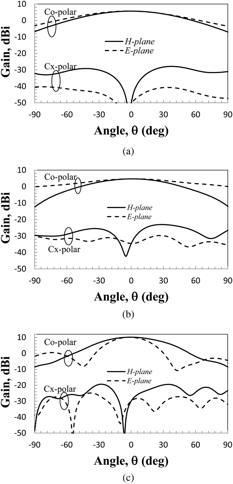
Fig. 3. Simulated radiation pattern of the slot-fed CDRA. (a) First mode at 2.78 GHz for Lmatch = 5 mm. (b) Second mode at 4.045 GHz Lmatch = 3 mm. (c) Third mode at 6.116 GHz Lmatch = 10 mm.
To show how the peak gains of these modes vary with Lmatch, an appropriate graph is generated for all the three modes as shown in Fig. 4. In the figure, only those values of Lmatch giving |Γin| < −10 dB for a mode are considered. It can be confirmed from Fig. 4 that for any Lmatch, the third mode provides the highest gain. The maximum gain for the third mode occurs at Lmatch = 10 mm, which also ensures insufficient excitation of the lower two modes as observed in Fig. 2. As the focus of this work is on achieving high gain, further investigations are restricted to the third mode only. It is known that the ground plane size can control the quality (gain and cross-polarization) of the radiation pattern of the CDRA [Reference Ojha and Kumar5]. So a suitable parametric study is conducted for the present DRA, and the ground size dependence of the peak gain and peak cross-polarization level for the third mode are plotted in Fig. 5. As seen, at around LG (or WG) = 70 mm (~1.4 λ 0 at the resonant frequency), the co-polar gain is a global maximum while the cross-polar gain is a global minimum as followed by the fundamental HEM11δ mode [Reference Ojha and Kumar5].

Fig. 4. Simulated peak gains versus Lmatch for the three modes of the CDRA (CDR: ɛr = 24, tanδ = 0.002, 2a = 19.43 mm, and d = 7.3 mm).

Fig. 5. Simulated peak gain versus ground size for the third (high gain) mode for Lmatch = 10 mm (CDR: ɛr = 24, tanδ = 0.002, 2a = 19.43 mm, and d = 7.3 mm).
Identification of the modes
As the first step of identifying the CDRA modes, the simulated radiation patterns in Fig. 3 are analyzed. Patterns of the first two modes (Figs 3(a) and 3(b)) share the common nature that the co-polar pattern in the H-plane is narrower, and the cross-polar level in the H-plane is higher, relative to those in the E-plane. The above features are typical to the HEM11p+δ modal family that radiate like magnetic dipole [Reference Mongia and Bharita8–Reference Feng and Leung10]. It is further verified from the near-field plots of the DRA that the first resonance (~2.8 GHz) corresponds to the HEM11δ mode. But the near-field analysis of the second resonance (~4 GHz) revealed that this mode also was appearing like the HEM11δ mode from the top view but was strongly perturbed by the slot field in the side view. So this mode may be called HEM11δ-like mode. This mode can alternatively be treated as contributed by the slot-loaded DR with a resonant frequency given by:

where c is the light speed in vacuum, L s = 10 mm, ɛrav is the average dielectric constant between the substrate (ɛr = 4) and the DR (ɛr = 24).
The calculated resonant frequency is in very good agreement with that simulated in HFSS (4.045 GHz). As the slot is an inefficient radiator compared to the DRA, the gain of this mode is lower than that of the fundamental HEM11δ mode of the DRA. Through proper optimization of the slot and the CDR parameters, the gain of the second mode may be improved for practical use. Now the radiation of the third mode (Fig. 3(c)) can be seen to exhibit some distinct features compared to the lower modes such as (i) the patterns are more directional; (ii) the pattern is broader in the H-plane than in the E-plane; (iii) the E-plane pattern has two dips at around ±45°.
These features imply a different modal family; to identify which near-field distributions of the electric (E) fields in the DRA at 6.116 GHz are generated using HFSS, as in Fig. 6(a). Corresponding schematic illustrations are shown in Fig. 6(b) along with that of the well-known HEM11δ mode. Two planes of the DRA are selected to analyze the field distributions – the top face (xy-plane) and the side face (xz-plane along x-x’). From the top face (Fig. 6(a)), the mode resembles some higher order HEM11p+δ mode which is a contradiction to the inference drawn from the radiation pattern analysis. However, on the side face of Fig. 6(a), three λ/2 field variations (indicated by three full-loops) along the diameter are visible. Finally, as shown in Figs 6(a) and 6(b), in the axial (z) direction, there is one λ/4 variation of the field (half-loop). Further by comparing the above said field variations with that of the HEM11δ mode, the third mode can be designated as HEM13δ mode. It should be noted that for the HEM1mp+δ mode, definitions of the diametrical (m) and the axial (p + δ) indices are different, for odd m (1, 3, 5, etc.) and even m (2, 4, 6, etc.).

Fig. 6. Simulated near-field vector distributions of the high gain (HEM13δ) mode at 6.116 GHz (CDR: ɛr = 24, tanδ = 0.002, 2a = 19.43 mm, and d = 7.3 mm, Lmatch = 10 mm, LG = WG = 70 mm). (a) Electric (E) field from HFSS. (b) Schematic illustrations of the electric field distributions of the (i) HEM11δ mode and (ii) HEM13δ mode.
Experimental verification
Fabricated prototype of the CDRA (ɛr = 24, 2a = 19.43 mm, a/d = 1.3) is shown in Fig. 7. Antenna characterization is performed with a VNA (Keysight N9928A), power meter (Agilent E4418B), function generator (Keysight N5173B), and a standard anechoic chamber.

Fig. 7. Fabricated prototype of the slot-fed CDRA. (a) Top view showing the slot. (b) Bottom view showing the microstrip (CDR: ɛr = 24, 2a = 19.43 mm, d = 7.3 mm, tanδ = 0.002; substrate: LG = WG = 70 mm, t = 1.6 mm, ɛr = 4, tanδ = 0.02; slot: LS = 10 mm, WS = 1 mm, Lmatch = 10 mm).
Measured and simulated reflection coefficients of the CDRA are compared in Fig. 8. Acceptable agreement is observed between the two curves. In both simulation and measurement, the first mode is excited weakly at ~2.8 GHz, and the second mode at ~4 GHz is totally disappeared. The HEM13δ mode is excited at 5.997 GHz with a reflection coefficient |Γin| = −18 dB in measurement. Corresponding resonant frequency and |Γin| in simulation are 6.116 GHz and −28 dB, respectively. The impedance bandwidths are 1.13 and 1.28% in measurement and simulation, respectively. Measured radiation patterns in the two principal planes along with simulated patterns are shown in Fig. 9 which are in good agreement. Measured peak gain is 9.71 dBi which is close to the simulated peak gain of 10.16 dBi. The 3 dB beam width in measurement and simulation is, respectively, 35° and 34° in the E-plane, while it is 68° and 67°, respectively, in the H-plane. The observed mismatches between the simulated and the measured results (Figs 8 and 9) are caused by the fabrication and alignment errors of the slot-fed DRA [Reference Guha and Kumar4], and/or the errors in the pattern measurement. The former error is responsible for the 10 dB difference between the simulated and the measured resonant dips (Fig. 8) which needs compensation.

Fig. 8. Input reflection coefficient versus frequency for the slot-fed CDRA (Fig. 7).

Fig. 9. Radiation patterns for the slot-fed CDRA at 6.116 GHz (simulated) and 5.997 GHz (measured). (a) E-plane. (b) H-plane.
Effect of dielectric constant and aspect ratio of the CDR on the high gain mode
The dielectric constant (ɛr) and the aspect ratio (a/d) of the CDR play vital roles in deciding the resonant frequency, and to some extent the radiation pattern of DRAs too[Reference Long, McAllister and Shen1, Reference Mongia and Bharita8]. So it is important in the present analysis to relate the above parameters to the resonant frequency and the gain of the high gain mode of the CDRA. A parametric study is conducted in HFSS for the present CDRA by keeping the diameter constant (2a = 19.43 mm) and by varying the ɛr and the a/d of the CDR. In the initial simulation setup, the slot size is kept at 10 mm × 1 mm, the Lmatch at 10 mm, and the ground size at 70 mm side. For each combination of ɛr and a/d, the peak gain of the first few resonances is recorded, and for the resonance giving the maximum gain, corresponding mode is identified through near-field analysis. Then through fine adjustments of the ground size and Lmatch, the impedance matching and the peak gain of the high gain mode are optimized. Corresponding resonant frequencies and gains are tabulated in Table 1. For comparison, the ratio of the resonant frequencies of the high gain mode and the corresponding fundamental mode (HEM11δ) is also listed in the table. In Table 1, for DRAs with a/d = 1, the near-fields are found to be a combination of two or more DRA modes. Such modes are indicated with the nomenclature of the closest resembling mode suffixed with “like”. It can be inferred from Table 1 that, CDRs with a/d > 1 favor the HEM13δ mode that resonates at about 2.2 times the resonant frequency of the HEM11δ mode and exhibits a gain more than 8 dBi for any CDR under study. The above aspects of the HEM13δ mode, in combination with equation (1) can be used for the rough estimation of the resonant frequency of the mode.
Table 1. Resonant frequencies and peak gains of the high gain mode of the CDRA for various dielectric constants (ɛr) and aspect ratios (a/d) of the CDR for 2a = 19.43 mm

a These modes are difficult to be identified correctly, hence the term “like” is used with them.
Improved design for impedance matching
To improve the impedance matching of the DRA, a parallel (shunt) stub is used with the microstrip line as done for the higher order HEM12δ mode [Reference Guha, Gupta and Kumar13] as shown in Fig. 10. In the HFSS model of the present design, the stub width is kept the same as the slot width (WS = 1 mm). The stub length lstub is optimized to attain the best impedance matching for a given stub position dstub that is varied as dstub = 0, ±4, and ±9 mm with respect to the slot position. Here dstub = 0 mm refers to the slot position, while dstub = 9 mm refers to the open end of the microstrip line. Corresponding variations in the reflection coefficients shown in Fig. 11 reveal that at dstub = 0 mm and lstub = 4 mm, the best impedance matching of |Γ|min = −49 dB is achieved. This implies ~21 dB better matching compared to that of the original CDRA (Fig. 8). The new resonant frequency is 6.125 GHz which is almost identical to the original frequency of 6.116 GHz.

Fig. 10. Schematic representation of the improved slot-fed CDRA with stub matching (other parameters as in Fig. 7).

Fig. 11. Simulated reflection coefficients of the slot-fed CDRA for different stub location (dstub) and stub length (lstub).
Experimental verification of the improved design
The fabricated model of the CDRA with stub loading is shown in Fig. 12 and the loaded stub as the inset. Measured reflection coefficient of the improved CDRA, relative to the original CDRA (Fig. 7), is shown in Fig. 13. In Fig. 13(a), the effect of stub loading is clearly visible that it mainly improves the reflection coefficient at resonance from −18 dB (at 5.997 GHz) to −32 dB (at 5.981 GHz). It is demonstrated in Fig. 13(b) that the stub loading has not affected the weakly excited HEM11δ mode, owing to the selection of Lmatch = 10 mm for the feed.

Fig. 12. Fabricated prototype of the simple slot-fed CDRA. (a) Top view. (b) Bottom view (stub: dstub = 0 mm, lstub = 4 mm, other parameters as in Fig. 7).

Fig. 13. Measured versus simulated reflection coefficients of the slot-fed CDRA (Lmatch = 10 mm, dstub = 0 mm, lstub = 4 mm). (a) Upper band showing only the HEM13δ resonance. (b) Lower band showing weakly excited HEM11δ resonance.
Figure 14 shows the principal plane radiation patterns of the CDRA for the original design and the improved design. As expected, the pattern shape and the magnitude are preserved in the improved design. Table 2 compares the performance characteristics of the two CDRA designs which show decent matching between each other. In literature, the maximum gain achieved for a CDRA operated at a single mode is 9.5 dBi at 7.5 GHz for the HEM12δ mode [Reference Guha, Banerjee, Kumar and Antar12]. In the above work, the HEM12δ mode of a CDRA (ɛr = 10 and a/d = 1) is excited with a coaxial probe supported by a cavity loaded ground plane. The present design also demonstrates identical gain of 9.6 dBi (Table 2), but the cross-polar level of the present design is 6 dB lower compared to [Reference Guha, Banerjee, Kumar and Antar12], by virtue of the slot excitation. Additional simulations predict that the gain of the present design can be improved by 1 dB with the use of high-quality substrate such as Roger's RT/Duroid.

Fig. 14. Measured versus simulated radiation patterns of the slot-fed CDRA. (a) E-plane. (b) H-plane (simulation: 6.116 GHz for without stub, 6.125 GHz for with stub; measurement: 5.997 GHz for without stub, 5.981 GHz for with stub).
Table 2. Performance comparison of the slot-fed CDRA without and with the stub

Performance comparison of the proposed HEM13δ mode CDRA with the fundamental HEM11δ mode CDRA [Reference Guha and Kumar6], and the higher order HEM12δ [Reference Guha, Gupta and Kumar13] and HEM133 plus HEM123 [Reference Mrnka and Raida15] mode CDRAs, all producing broadside radiation and employing simple slot feed, is furnished in Table 3. The first point to observe is that the proposed mode is superior to both the HEM11δ mode [Reference Guha and Kumar6] and the HEM12δ mode [Reference Guha, Gupta and Kumar13], in terms of impedance matching, gain, and beam width. The gain of the proposed mode is lower than that of the HEM133 mode plus HEM123 mode [Reference Mrnka and Raida15] as the latter uses a combination of two similar modes, and also that its design uses a lower ɛr DRA (ɛr = 6.15). Also note that the bandwidth of the proposed CDRA is much smaller than that of any other design as the proposed design uses a high ɛr DRA, higher by a factor of about 2–4 than the other designs.
Table 3. Comparison of the measured performance of the proposed CDRA design with existing designs based on the slot feed

Conclusion
In this paper, the HEM13δ mode of a CDRA is excited with a simple microstrip slot for high gain broadside radiation. For a fabricated CDRA with dielectric constant ɛr = 24, diameter 2a = 19.43 mm, and aspect ratio a/d = 1.3, the HEM13δ mode is excited at 6 GHz with a reflection coefficient of −18 dB, peak gain of 9.71 dBi, and peak cross-polarization level of −24 dB. By loading a shunt stub on the feed line, the reflection coefficient of the above mode is reduced by 14 dB without notable variation in the rest of the radiation characteristics. The HEM13δ mode DRA may be proposed for DRA arrays due to its high gain, low cross-polarization, and ease of excitation. The low impedance bandwidth of the proposed DRA, inherent to the high dielectric constant−higher order mode operation, may be improved by using existing design principles [Reference Fang and Leung9, Reference Feng and Leung10, Reference Mrnka and Raida15]. This attribute is left for future work.
Acknowledgement
This work was supported by the Department of Science and Technology (DST), India, through the FIST program under Grant Ref: SR/FST/ETI-346/2013. The authors would like to thank Mahesh Chandra Saini for his assistance in the radiation pattern measurement, and the reviewers for their constructive criticisms.
 Anuj Kumar Ojha received his M.Tech degree in digital communication from Rajasthan Technical University (RTU), Kota Rajasthan in 2013. Later he joined the MEMS group at CSIR-CEERI Pilani, Rajasthan as the project fellow, where he worked on the development of silicon-based MEMS piezoresistive pressure sensors for various applications. He has published journal/conference papers on various aspects of MEMS sensors. Presently, he is pursuing the Ph.D. degree at the Department of Electrical and Electronics Engineering, Birla Institute of Technology and Science, BITS Pilani (Pilani campus), Rajasthan, India. His research interests include dielectric resonator antennas, higher order mode antennas, and sensors.
 A.V. Praveen Kumar received his Ph.D. degree in microwave electronics from the Department of Electronics, Cochin University of Science and Technology (CUSAT), Kerala in 2009. His thesis was on the fabrication, characterization, and development of dielectric resonators and its application in wideband dielectric resonator antennas. He joined the Engineering Department, Lancaster University, UK as a postdoctoral fellow where he worked on the development of radiofrequency cavities for particle accelerators. His major research interest is in RF and microwave engineering which includes antennas, cavity resonators, particle accelerators, and material characterization techniques. He has published several international journal/conference papers on various aspects of RF engineering. Presently, he is working as an Assistant Professor in the Department of Electrical and Electronics Engineering, Birla Institute of Technology and Science, BITS Pilani (Pilani campus), Rajasthan, India.


