I. INTRODUCTION
Thanks to the gated nature of the signal, ultra wide band impulse radio (IR-UWB) is a promising technology for ultra-low-power application. When efficient power gating techniques are used, the power consumption between two consecutive pulses can be highly reduced and the overall power consumption is scalable with the bit rate. Consequently, IR-UWB is a good candidate for ultra-low-power applications such as radio frequency identification (RFID), or autonomous wireless sensor network (WSN) in particular when localization capabilities are needed. For these applications, the need for (low cost) self or remotely powered communication systems is very high.
The design of an ultra-low-power communication system is a very challenging issue, especially concerning the radio-frequency front-end which generally consumes the greatest part of the power budget. For example, in a remotely powered RFID UHF transmitters commonly named passive TAGs, the available power is only about few micro-watts at 10 m from the reader and has to supply the TAG [Reference Karthaus and Fischer1]. In the case of a 10 cm2 photovoltaic harvesting system, the available power is around 100 μW under 100 lm (lumen) lighting which corresponds to a typical indoor environment. In both cases, the energy must be stored which is a major drawback. First, the use of an energy tank such as external capacitors or micro-battery (cell) increases the manufacturing cost. Second, the communication is turned off when the battery is charging which reduces the instantaneous bit rate. IR-UWB can resolve these issues since previous published works present fully integrated transmitters having a power consumption of few micro-watts [Reference Crepaldi, Li, Dronson, Fernandes and Kinget2]. Such power consumption allows the system to be always powered and lower than the constraint on the storage. Since it reduces the storage constraints and can be fully integrated, IR-UWB appears to be a good low cost solution for ultra-low-power applications.
Moreover, IR-UWB is also a promising technology for localization systems due to the high temporal resolution of the signal. Both localization and low cost are interesting properties for ultra-low-power applications such as RFID or WSN, but they need high energy pulses to be efficiently exploited. Indeed, high energy pulses increase the localization precision [Reference Guidi, Dardari, Roblin and Sibille3] and enable the use of a low cost non-coherent receiver [Reference Dehaese4]. Finally, to meet these application requirements, the transmitted energy must be increased while the energy consumed by pulse must be reduced. In other words, the energy efficiency of the transmitter must be increased as much as possible. Consequently, this energy efficiency appears to be the most significant figure of merit (FOM) in order to evaluate performance in such a context.
In this paper, we present the design of an ultra-low-power pulse generator providing high energy pulses. The power consumption and the energy efficiency have been optimized for ultra-low-power and low cost systems. In the first part, starting from the analysis of the FOM presented in the literature dedicated to pulse generators, a design strategy which optimizes the energy efficiency for a given low power application is presented. Then the proposed architecture, based on an integrated filter excitation technique, is described in Section III. Particular attention is paid to the power management and to the output dynamic. The last section presents measurement results of the pulse generator realized in a standard 130 nm CMOS technology.
II. POWER EFFICIENT TOPOLOGY
A) Figure of merit
For pulse generator design, the most often used FOM is the consumed energy per bit E C which is easily derived from the power measurement as follows:
 $${E_C} = \displaystyle{{{P_{DC}}@PRF} \over {PRF}},$$
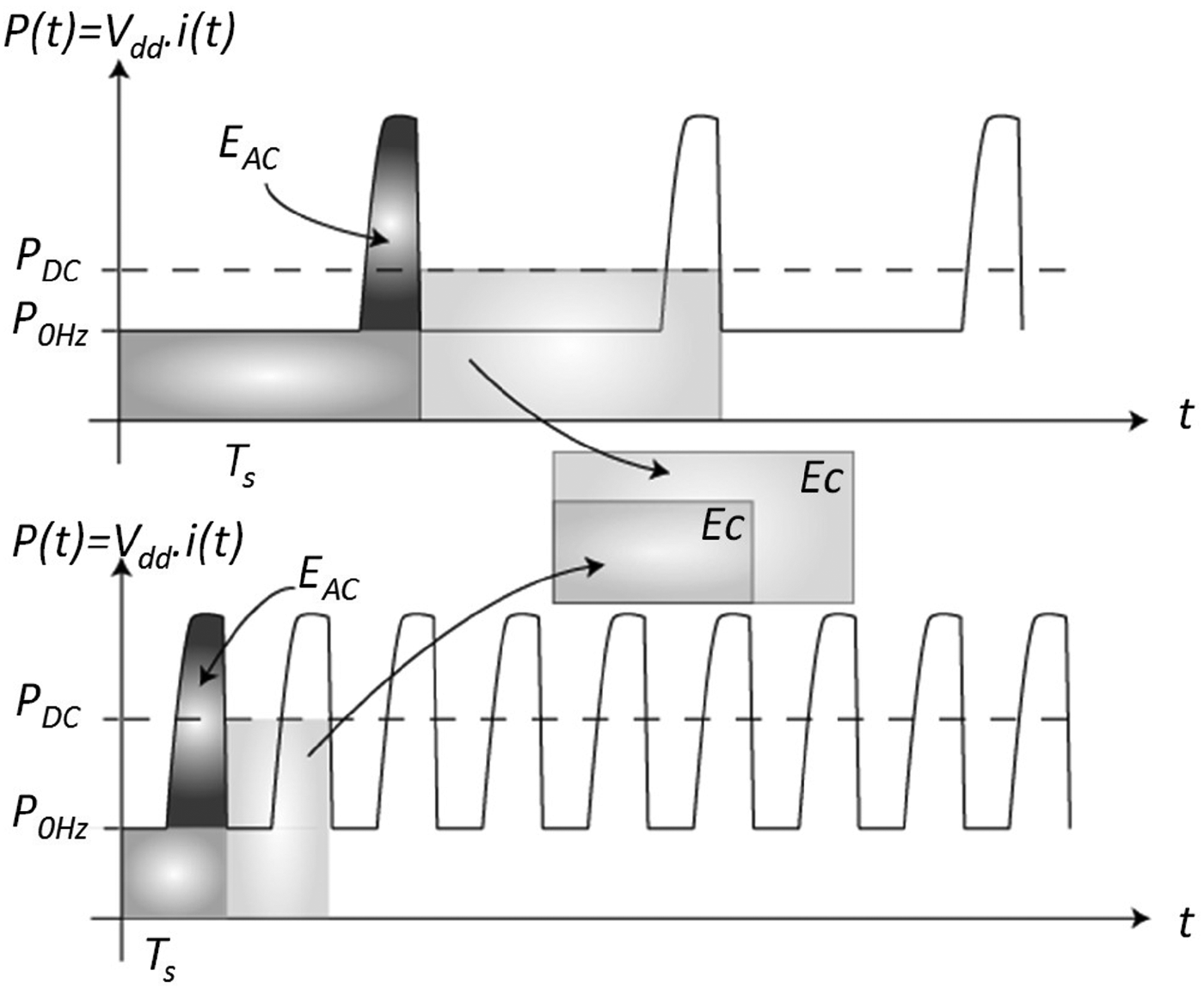
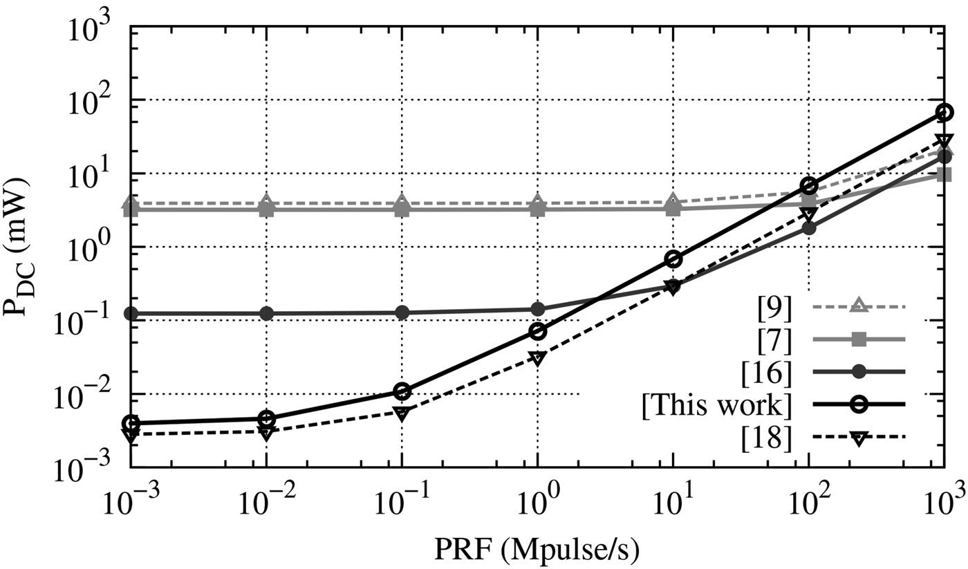
where PRF is the pulse repetition frequency and P DC@PRF the power consumption measured at a given PRF. In a practical implementation, due to leakage or biasing, some energy is consumed between the emission of two consecutive pulses and E C varies with PRF as shown in Fig. 1. It is therefore difficult to extrapolate from E C, the power consumption at any PRF and then to compare different architectures designed for different bit rates.

Fig. 1. Instantaneous consumed power.
To overcome this limitation, [Reference Wentzloff and Chandrakasan5] gives the power consumed at a PRF equal to 0 Hz (P 0 Hz) which represents the leakage power and the energy dynamically consumed by the generator (E AC). As shown in Fig. 1, these metrics give the power consumption as a function of the PRF as follows:
 $${P_{DC}}\left( {PRF} \right) = {P_{0Hz}} + {E_{AC}} \cdot PRF.$$
These FOM are interesting since they give the power consumption at any bit rate. Moreover, these FOM can be easily extracted from measurements since P DC linearly varies with PRF.
However, this FOM has some limitations. Since it does not take the emitted power P E into account, it is not possible to compare pulse generators that produce pulses with different energies. It is then relevant to evaluate the power efficiency which is finally equal to the energy efficiency shown as follows:
 $$\eta \left( {PRF} \right) = \displaystyle{{{P_E}} \over {{P_{DC}}}} = \displaystyle{{{E_P} \cdot PRF} \over {{E_C} \cdot PRF}} = \displaystyle{{{E_P}} \over {{P_{0Hz}}/PRF + {E_{AC}}}},$$
where E P is the energy of the emitted pulse. This FOM can also be obtained from measurement data (E P=P E/PRF). Due to the frequency limitation of some topologies, E P can decrease with the PRF. This FOM enables this effect to be taken into account.
B) Design strategies
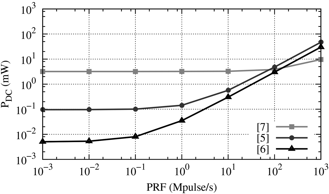
Figure 2 presents the power consumption of different published pulse generators. The authors [Reference Wentzloff and Chandrakasan5, Reference Dokania, Wang, Tallur, Dorta-Quinones and Apsel6] principally use CMOS digital circuits which have no DC power consumption. This leads to a low P 0 Hz which is mainly due to leakage current (96 and 5 μW for [Reference Wentzloff and Chandrakasan5, Reference Dokania, Wang, Tallur, Dorta-Quinones and Apsel6], respectively). It appears that a low P 0 Hz performs best at low rate and leakage is one of the main issues in this context. In [Reference Bourdel7], differential MOS Current Mode Logic cells are used. This gives a high DC power consumption (3.2 mW@0 Hz) and a small E AC (6.4 pJ/pulse) compared to other works (47 and 30 pJ/Pulse for [Reference Dehaese4, Reference Dokania, Wang, Tallur, Dorta-Quinones and Apsel6], respectively) since differential structures do not consume dynamic current. Figure 2 clearly shows that this topology performs better for PRF higher than 100 MHz and that reducing E AC is the main issue for the design of high speed (HS) pulse generators.
Fig. 2. Power consumption of several published pulse generators.
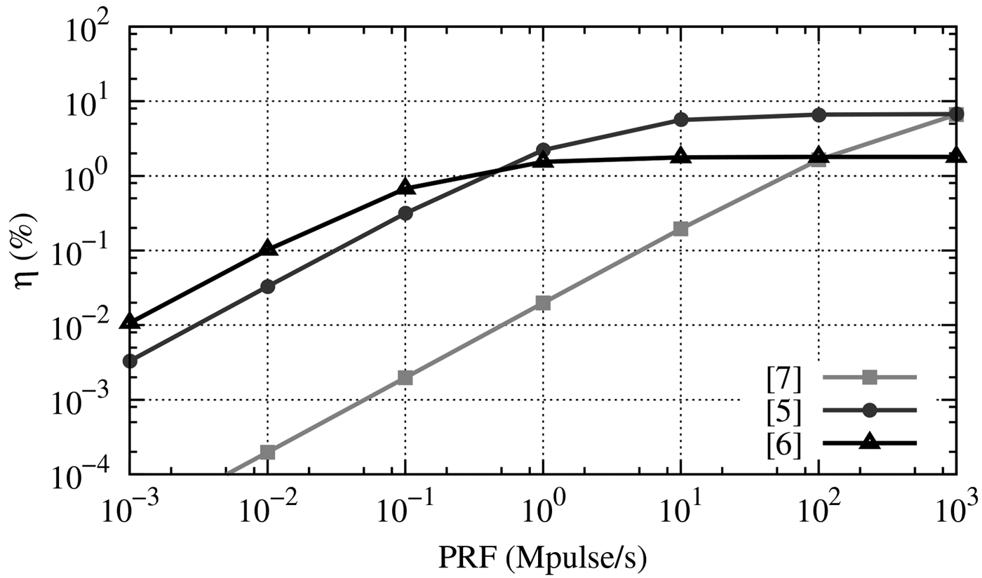
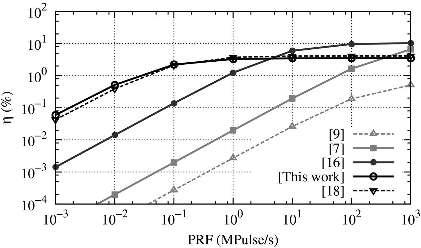
The efficiency is given by (3) and shows relevant information. In Fig. 3 the efficiency is plotted as a function of the bit rate for the same generators as in Fig. 2. Since E P is rarely given, it has been approximated using (6) and (7). For a better approximation, the effect of the pulse envelope on the energy is taken into account. Depending on the pulse shape, the pulse is modeled by a sine wave modulated by square function (4) or by a Gaussian pulse transposed at the center frequency f M of the pulse (5).
 $${p_S}(t) = A\sin (2\pi {f_M}t){\pi _\tau} (t),$$
 $${p_G}(t) = A\exp ( - a{t^2})\cos (2\pi {f_M}t).$$
Fig. 3. Energy efficiency of several published pulse generators.
The energy of the pulse can then be easily derived from the maximum value of the pulse A and its width τ as follows:
 $${E_{PS}} = \displaystyle{{{A^2}} \over {{Z_L}}}\left[ {\displaystyle{\tau \over 2} - \displaystyle{{\sin (2\pi {f_M}\tau )} \over {4\pi {f_M}}}} \right],$$
 $$\eqalign{&{E_{PG}} = \displaystyle{{{A^2}} \over {2{Z_L}}}\sqrt {\displaystyle{\pi \over {2a}}} \left[ {1 + \exp \left( { - \displaystyle{{{{\left\vert {4\pi {f_M}} \right\vert}^2}} \over {8a}}} \right)} \right] \quad {\rm with} \cr & \quad a = \displaystyle{{{\pi ^2}BW_{ - X\,{\rm dB}}^2} \over {2\ln \left( {{{10}^{X\,{\rm dB}/10}}} \right)}}},$$
where Z L is the load impedance of the pulse generator and BW −XdB the –X dB bandwidth. An analysis of the efficiency gives interesting information for the design strategies. The authors [Reference Wentzloff and Chandrakasan5] achieve a higher output dynamic A than [Reference Dokania, Wang, Tallur, Dorta-Quinones and Apsel6] which consequently increases the dynamic consumed energy E AC. It is a drawback when only the power consumption is considered but, as shown in Fig. 3, the efficiency is finally higher for bit rates higher than a few MHz. It also appears that maximizing the output dynamic is an important issue when high efficiency is needed, even if it is at the cost of an increased E AC.
Based on these observations, the presented design will first focus on leakage current reduction methods to address ultra-low-power and low rate applications. Secondly, the output dynamic will be maximized (at the cost of an increased E AC) to improve the efficiency and also to optimize the power budget which is an important issue in low power applications.
C) Architecture choice
Among the different techniques used for pulse generation, ON/OFF local oscillator (LO) and filter excitation are the most promising topologies to reduce power consumption. To maximize the output dynamic and the bandwidth in ON/OFF LO, the LO start time must be as small as possible and an inverter based ring oscillator should be preferred [Reference Sim, Kim and Hong8]. With such topology, CMOS technology can be used which reduces the P 0 Hz. ON/OFF LO technique highly reduces the P 0 Hz since the LO is turned on only during the pulse duration. To be fully efficient, the power amplifier or the antenna driver must be power managed [Reference Phan, Lee, Krizhanovskii, Le, Han and Lee9, Reference Barras, Ellinger, Jackel and Hirt10]. To reduce further the time conduction of the active cells, it is possible to use filter excitation. With such a technique, a very short baseband pulse is used to excite a filter to produce its impulse response. Here, the conduction time of the active cells is around 100 ps [Reference Bourdel7] and is independent of the pulse bandwidth BW whereas in ON/OFF LO it depends on 1/BW. A short time conduction of the active cells limits E AC and improves the efficiency. Moreover, the filter excitation technique can achieve large amplitude pulses which lead to high E P. It also facilitates the integration and the packaging process [Reference Bourdel, Gaubert, Fourquin, Vauche and Dehaese11]. At last, the filter excitation well suits the generation of sub-nanosecond duration pulses needed to reach high localization precision [Reference Bourdel7].
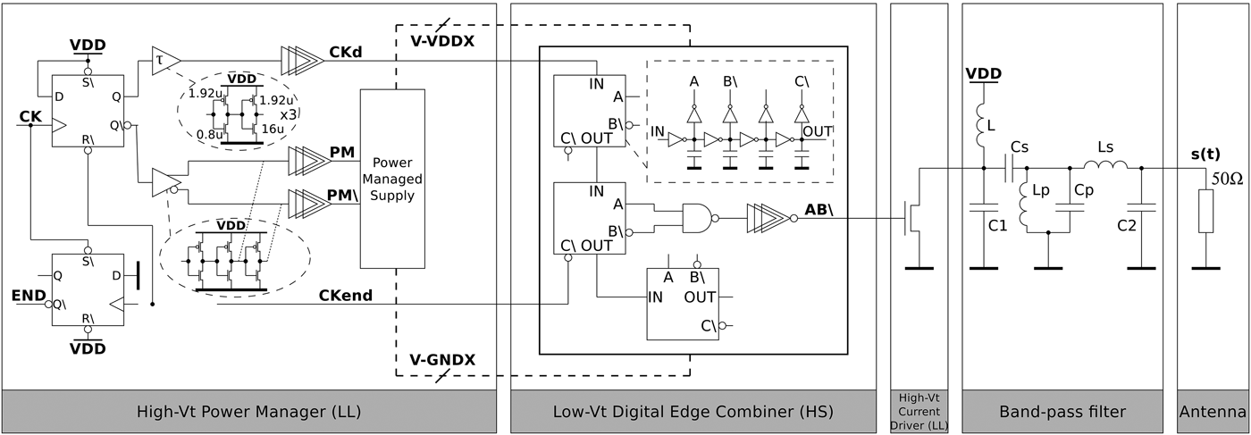
The proposed architecture is based on an integrated filter excitation technique and the principle is given in Fig. 4. The baseband pulse used to excite the filter is generated by a Low-Vt Digital Edge Combiner implemented with CMOS logic cells. To reduce the leakages, a high-Vt managed power supply (MPS) which control managed power lines (V-VDDX and V-GNDX) is used. The filter is a passive fully integrated circuit and is driven by a C class amplifier to reduce P 0 Hz consumption.
Fig. 4. Proposed pulse generator principle.
III. PULSE GENERATOR DESIGN
The pulse s(t) produced by the excitation filter technique is the response of the filter to a baseband pulse π τ(t). The expression of s(t) and its Fourier transform are given by:
 $$s(t) = \displaystyle{B \over {\sqrt l}} \cdot {\pi _\tau} (t) \times {h_E}(t),$$
 $$S(f) = \displaystyle{{B\tau \sin c\left( {\pi \tau f} \right) \cdot {H_E}(f)} \over {\sqrt l}}, $$
where l represents the power loss of the filter, H E(f) the normalized transfer function of the filter, B the magnitude of the basesband pulse and τ its time duration. The main characteristics of the pulse are given by the baseband pulse (through B and τ) and by the filter impulse response. This technique has been widely presented and a detailed sizing method is given in [Reference Bourdel7]. In this design, we use a third-order Bessel–Thompson filter driven by a 1.2 V magnitude and 75 ps width baseband pulse. A standard CMOS 130 nm technology is used.
A) Power management system
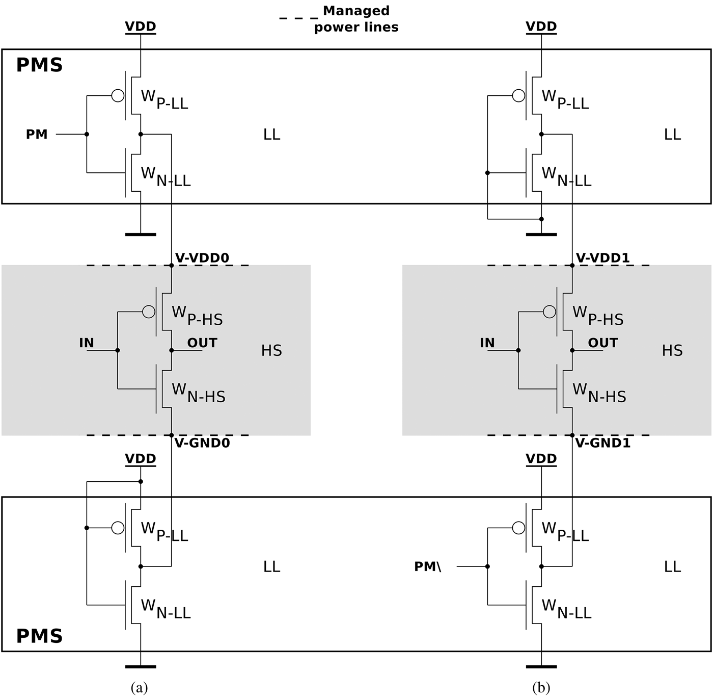
The aim of the power manager is to reduce the leakage current when no pulses are generated. Several techniques have been proposed to reduce leakage current of CMOS logic circuits. A first technique named VTCMOS consists in applying different bias voltages to the substrate depending on the operating mode of the cell [Reference Keshavarzi12]. When the cell is off, the substrates of the NMOS transistor (resp. PMOS) can be for example connected to VDD (resp. GND) in order to increase (resp. decrease) the threshold voltage Vt and thus limiting the leakages. A second technique (DTCMOS) consists in dynamically changing the threshold voltage when the circuit is commuted [Reference Assaderaghi, Parke, Sinitsky, Bokor, Ko and Hu13]. In the CMOS inverter case, the gates of the PMOS and NMOS are connected to the substrate. For both VTCMOS and DTCMOS, an isolated substrate is needed and triple-well or SOI technologies must be used which increase the manufacturing cost. A third solution is to use a multi-Vt CMOS technology [Reference Wei, Chen, Roy, Johnson, Ye and De14] which provides transistors having different threshold voltages. Most of the standard CMOS technologies offer low leakage (LL) transistors having high-Vt and HS transistors having low Vt. The proposed power manager uses a multi-Vt-CMOS approach where LL transistors are used to power supply the HS transistors which are used to implement the Low-Vt Digital Edge Combiner.
The elementary inverter used in the design of the Digital Edge Combiner is presented in Fig. 5. The NMOS and PMOS HS transistors have respectively their bulks connected to GND and VDD whereas their sources are respectively connected to the managed power line V-GNDX and V-VDDX provided by the MPS. The MPS is based on LL inverters which are sized in order to deliver the same drain source current I DS than the HS transistors. Since I DS is a linear function of the saturation current density J SAT (A.m−1) and of the MOS width W [Reference Sakurai and Newton15], the required size of the LL is given by:
 $${W_{LL}} = \displaystyle{{{J_{SAT - HS}}} \over {{J_{SAT - LL}}}} \cdot {W_{HS}},$$
where the NMOS, or the PMOS transistors of the HS and LL inverters can be considered.
Fig. 5. Inverter set to 0 (a) and set to 1 (b) in the idle state with its associated MPS.
The idle state of the HS inverter output defines the signal to be connected at the input of the LL inverter of the MPS. When the idle state is 0, the LL inverter input which provides V-GNDX is connected to VDD and the LL inverter input which provides V-VDDX is connected to PM since it is the power management signal active on the high state provided by MPS. When the idle state is 1, the LL inverter input which provides V-GNDX is connected to PM\ and V-VDDX is connected to GND. Thus, when power management is active (PM=1), HS inverter is short-circuited since its V-GNDX, V-VDDX and also OUT are equal to the same voltage. In this case, the total leakage depends only on twice the sum of leakage current of the LL inverter which is much lower than the HS inverter leakage for an equivalent saturated current. The gain g OFF on the leakage power P 0 Hz achieved by this power management technic only depends on the saturation current density J SAT of the LL and HS transistor and is given by:
 $${g_{OFF}} = \displaystyle{{{J_{OFF - HS}} \cdot {W_{HS}}} \over {2 \cdot {J_{OFF - LL}} \cdot {W_{LL}}}} = \displaystyle{{{J_{OFF - HS}} \cdot {J_{SAT - LL}}} \over {2 \cdot {J_{OFF - LL}} \cdot {J_{SAT - HS}}}},$$
where J OFF is the linear leakage current density (A/m) of the considered MOS transistor. It clearly appears that the proposed power management technic has benefits only when the ratio between J SAT and J OFF of the LL inverters is greater than twice the one of the HS.
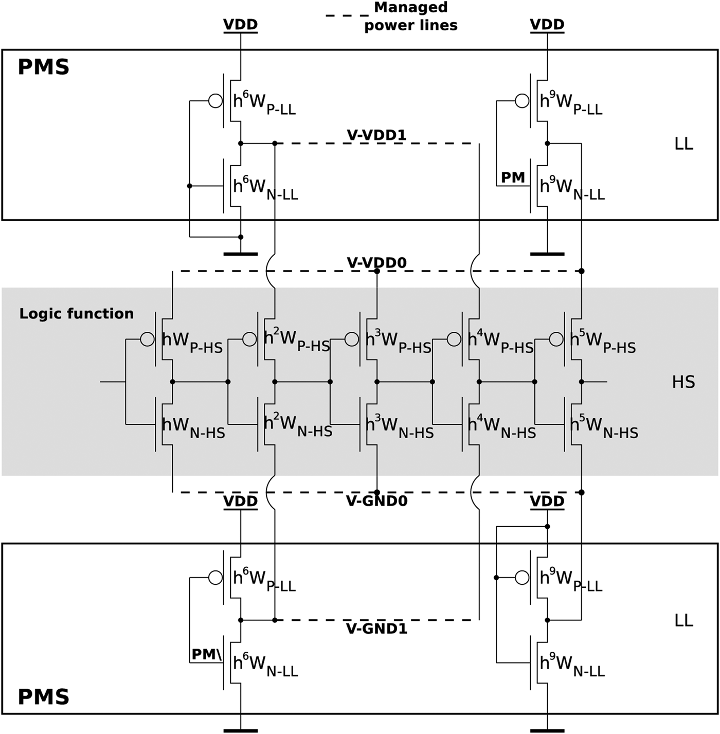
In the case of a more complex logic function such as the inverter chains used in the edge combiner or in the power manager, a particular focus has to be done on the chosen idle state of each stage which composes the function. Here the idle states have to be alternatively 0 and 1 in order to keep coherent logic states with the realized logic function inside each HS stage as shown on Fig. 6 where an inverter chain with a growth factor of h is represented. To reduce the complexity, LL inverters with an identical input signal can be merged in order to simplify the final circuit. To limit the current driven by each inverter and to improve the decoupling, the LL inverters are split into several parts which are distributed all along the power line.
Fig. 6. Inverter chain with MPS.
B) Edge combiner
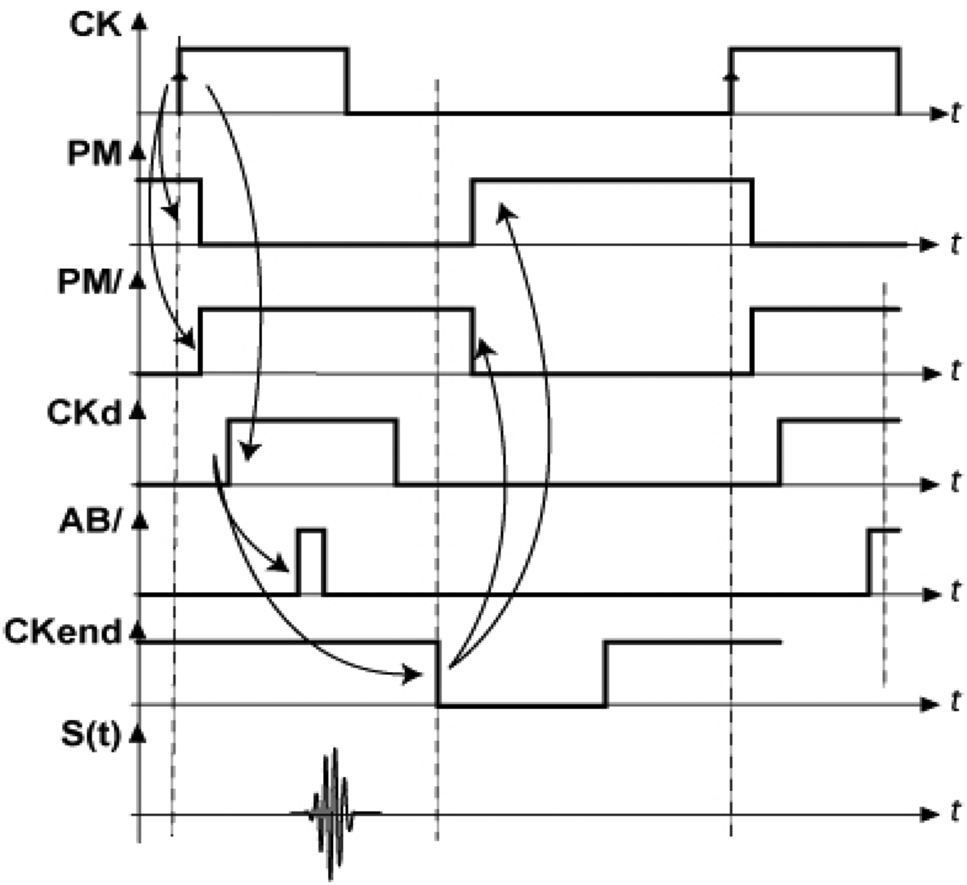
The edge combiner used has to generate the baseband pulse required by the filter excitation technique when a rising edge appears on CK. Then, CK is used to set PM and PM\ to GND and VDD, respectively, and then to control the MPS. As shown in Fig. 7, CK is delayed (CKd) before being provided to the edge combiner in order to ensure that the circuits are turned on when the signal is applied to the input. CKd is propagated through a delay line. Two consecutive edges (A and B\) are combined to produce the baseband pulse needed to excite the filter. CKd is further delayed to produce the signal (CKend) which is used by the power manager to shut down the power lines. The edge combiner uses only CMOS logic gates implemented with HS transistors and driven by the MPS. The baseband pulse is produced by using a simple CMOS NOR gate based on inverters designed as described above. A driver based on an inverter string is inserted at the output to match the small transistors (W=10 μm) used in the NOR gate with the large ones used in the filter driver.
Fig. 7. Main signal chronograms.
C) Band pass filter and filter driver
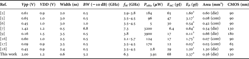
The band pass filter is a Bessel–Thompson filter. This filter is chosen because a third order is sufficient to match the FCC mask. Low order reduces the number of inductors needed and then reduces the loss in the filter which finally maximizes the E P. The filter must be carefully designed and the interconnected wires must be shortened during the layout realization to limit loss. The parasitic capacitances of the inductors must be compensated to avoid the degradation of the filter impulse response and to ensure that the pulse complies with the FCC mask. Among the different possible filter structures, the one chosen offers many advantages. The first resonator (L-C1) can be used to bias the filter driver. Cs achieves a DC isolation and C2 can be used to compensate the pad capacitance. Moreover, Cp can be reduced to compensate the parasitic capacitance of Lp. Cp and Cs can be reduced to compensate that one of Ls and C1 can be reduced to compensate both the output capacitance of the filter driver and the parasitic capacitance of L. The filter is driven in a current mode in order to achieve a pulse magnitude greater than the supply voltage on the 50 Ω input impedance of the filter. The driver is a class C amplifier to avoid power consumption when no pulse is generated. To further reduce the leakage, a LL transistor is used. The width of the transistor M1 is tuned to maximize the energy efficiency given by (3) which leads to a value of 560 μm. The main parameters of the filter design are summarized in Table 1.
Table 1. Main design parameters summary.

IV. MEASUREMENT RESULTS
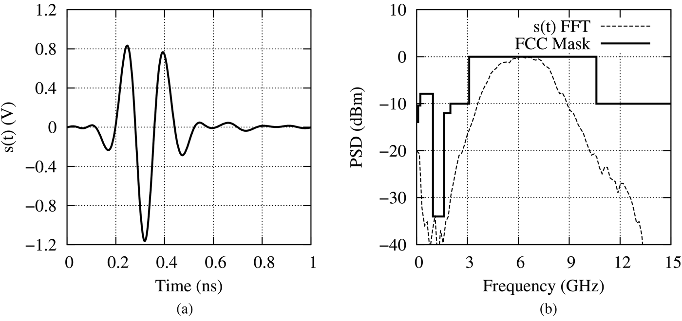
The pulse generator has been designed with a 0.13 μm standard CMOS technology from ST Microelectronics. The die is shown in Fig. 8 and its area is 0.56 mm2. The measured time and normalized frequency responses of the generated pulse are given in Fig. 9. The −10 dB bandwidth (BW−10 dB) is 5.22 GHz and is centered on 6.25 GHz. The very wide bandwidth of the pulse leads to a very short time duration equal to 0.6 ns which is a large benefit for localization precision but a major drawback for the emitted energy. The pulse magnitude is 2 Vpp and produces high pulse energy although the duration of the pulse is short. The measured energy of the emitted pulse is 2.15 pJ whereas the approximation given by (7) is 2.37 pJ which confirm the accuracy of this approximation.
Fig. 8. Die photograph of the proposed pulse generator.
Fig. 9. Measurement of the time response (a) and the frequency response (b).
The static leakage current is equal to 3.26 μA which leads to a power leakage P 0 Hz of 3.91 μW for a voltage supply of 1.2 V. Half of the power leakage is due to the filter driver. The measured power consumption is plotted for different PRF in Fig. 10 and is identical to the one obtained (2). The performances are compared with previous works in Fig. 10. The power consumption is only 3.98 μW@1 kb/s and 10.7 μW@100 kb/s which is well suited for ultra-low-powered applications. The value of E AC is extracted from this measurement and is 68 pJ. Most of the consumed dynamic energy is due to the inverter string needed to match the edge combiner with the filter driver. In Fig. 11, the efficiency is plotted as a function of the PRF as introduced in (3) and is compared to previously published works which are summarized in Table 2. The pulse generator also exhibits good efficiency at low rates (0.06%@1 kb/s and 2.22%@100 kb/s).
Fig. 10. Measured power consumption as a function of the PRF.
Fig. 11. Estimated efficiency as a function of the PRF.
Table 2. Performance summary of the proposed pulse generator and comparison with previous works.
V. CONCLUSION
The design of an ultra-low-power and high efficient pulse generator has been presented. The topology has been carefully chosen to achieve good performances at low rates. It is demonstrated that the filter excitation technique can generate very short 2.15 pJ pulses which can be helpful for high precision location applications. Associated to a power management technique which reduces leakage current, this topology demonstrates also low power capabilities (3.98 μW@10 kb/s) and could be used in ultra-low-power systems.
Remy Vauche got into preparation for the competitive entrance examinations to French Engineering Schools, Metz, France, in 2003. He received his M. Eng. degree in Microelectronics and Telecommunication from Polytech’ Marseille, and the M.S. degree in Microelectronics and Nanoelectronics from Aix-Marseille University, Marseille France, in 2008. He received the Ph.D. degree in Microelectronics from the University of Provence, Aix-Marseille I, France, in 2011. From 2011 to 2014, he was an Assistant Professor in the ISEN French Engineering School, Toulon, France. Since 2014, he is now an Assistant Professor of the Aix-Marseille University, Marseille, France, and a member of the Integrated Circuits Design Team from the Provence Nanosciences Microelectronics and Materials Laboratory (IM2NP), Marseille, France. His current field of research is in the design of UWB pulse generators for low-cost applications.
Sylvain Bourdel received the Ph.D. in Microelectronics from the National Institute of Applied Science (INSA) of Toulouse in 2000. He was with the LAAS laboratory of Toulouse where he was involved on radiofrequency systems modeling and he was particularly focused on spread spectrum techniques applied to 2.45 GHz transceivers. In 2002, he joined the IMNP in Marseille where he headed with Pr H. Barthélemy the Integrated Circuit Design Team of the IM2NP. He joined in 2013 the Grenoble-INP as a full Professor where he works at the IMEP-LAHC laboratory. He works in CMOS RF IC design and integration. He particularly focuses on low-cost applications including RFID, UWB, and narrow band systems. His area of interest also includes system level specifications, system packaging, and interconnections.
Nicolas Dehaese received the M.S. degree from the ISEN engineering school, Lille, France, in 2002 and the Ph.D. degree in Electronics from the University of Provence, Aix-Marseille I, France, in 2005. Since 2006, he is an Assistant Professor in the Integrated Circuits Design Team from the Provence Nanosciences Micro-electronics and Materials Laboratory (IM2NP), Marseille, France. His current field of research is in the design of analog/RF CMOS integrated circuits and system level specifications for low-cost applications including narrow band (2.4 GHz) and ultra wideband (3.1–10.6 GHz) systems.
Jean Gaubert received the M.S. and the Ph.D. degrees in Applied Physics from Paul Sabatier University, Toulouse, France, in 1985, and 1988, respectively. From 1989 to 2001, he was an Assistant Professor at the Ecole Nationale Supérieure de l'Electronique et de ses Applications, Cergy-Pontoise, France, where he was involved with high-speed GaAs and InP bipolar devices modeling. In 2001, he joined the University of Provence, Marseille, France, and the Institut Matériaux Microélectronique Nanosciences de Provence (IM2NP). His research focuses on the design and integration of RF/Microwave CMOS integrated-circuits and systems for wireless communications. He has published more than 60 refereed journal and conference papers.
Oswaldo Ramos Sparrow was born in Lima, Peru, in 1984. He was studied Engineer Electronic at Ricardo Palma University in Lima-Peru. He received the M. Eng. degree in Microelectronics and Telecommunication from Polytechnique Marseille, France in 2010 and the M.S. in micro-electronics and nanoelectronics from Aix-Marseille University, Marseille France, in 2011. He is currently working toward the Ph.D. degree at the University of Nice-Sophia Antipolis, France. His current research interests include UWB radio transceiver modeling and design in 0.13 lm CMOS technology for low-power and low-cost applications.
Eloi Muhr was born in Reims, France, in 1989. He received his M.S. degree in Microelectronics and Nanoelectronics from Aix-Marseille University, Marseille France, in 2012. He is currently a Ph.D. student of Aix Marseille University with the IM2NP laboratory. His current research interests include CMOS UWB radio transceiver design and programmable UWB system.
Herve Barthelemy received the M.Sc. degree in Electrical Engineering in 1992 and the Ph.D. degree in Electronics from the University of Paris XI Orsay, France in 1996. In 2002, he received the HDR degree from the University of Provence, Aix-Marseille I, France. From 1996 to 2000 he was an Assistant Professor at the Institut Supérieur d'Electronique de la Méditerranée (ISEN) in Toulon, France. In 2000 he joined the University of Provence where he has been a full Professor since 2005. In 2007 He joined the University of Sud-Toulon-Var. Since 2005 he headed the Integrated Circuits Design Team at the IM2NP. The team has 12 researchers and Ph.D. students involved in several research projects with industry. His research interests are mainly in the design of radiofrequency analog integrated circuits. He authored and co-authored multiple publications in international journals and conference proceeding.