


Introduction
The next-generation wireless communication infrastructure demands for high flexibility, low cost, and high efficiency [1]. This goes along with growing needs for wideband, multi-band, and multi-standard features. As a consequence, in the last years, increasing research efforts have been devoted to non-analog power amplifier (PA) realizations (e.g. [Reference Nakamizo, Mukai, Shinjo and Gheidi2–Reference Wentzel, Chevtchenko, Kurpas and Heinrich4]), paving the way to an all-digital transmitter chain shown in Fig. 1.

Fig. 1. Block diagram of a digital transmitter chain.
In this concept, the usual upconverter is replaced by a digital modulator. The modulator accepts any kind of a complex baseband signal and translates it in a binary pulse sequence so that the only analog components left is a bandpass filter (filter in Fig. 1) at the PA output just before the antenna. As a consequence, the PA becomes a pure switch. On the base-station side, the required combination of high-speed switching with high power capabilities puts great challenges on the transistor performance, but nowadays the GaN technology offers solutions here.
Future wireless communication standards will be based on very broadband signals with high peak-to-average power ratios (PAPR) in the 10–12 dB range. This is responsible for one of the most crucial problems of the digital PAs up to now, the significant degradation of efficiency at high power back-off (PBO) values [Reference Nakamizo, Mukai, Shinjo and Gheidi2, Reference Wentzel, Chevtchenko, Kurpas and Heinrich4]. The values achieved so far [Reference Hoffmann, Wentzel, Hühn and Heinrich5] are not fully competitive to analog concepts like Doherty [Reference Kim and Park6] or envelope tracking [Reference Wolff, Heinrich, Berroth and Bengtsson7].
Outphasing is a concept of improving efficiency at high PAPR values, which is well-known from analog PAs. It has been applied to digital PAs as well [Reference Ding, Hur, Banerjee, Hezar and Haroun8–Reference Sen11], but up to now, this was done only for PAs with small output power P out levels, below [Reference Ding, Hur, Banerjee, Hezar and Haroun8] or around 1 W [Reference Fritzin, Svensson and Alvandpour10], or at low frequencies (30…600 MHz) [Reference Sen11].
This paper presents for the first time a digital outphasing PA (DOPA) for the 800 MHz band with output powers above 5 W. It is intended for base station applications, reaching a low-efficiency drop over a wide range of PBO. This is achieved by applying a circuit topology for resonant commutation to both final stages, similar to that shown in [Reference Ding, Hur, Banerjee, Hezar and Haroun8]. The outputs of both amplifier branches are combined with two discrete inductors; no transformer or space-consuming elements such as high-Q filters are required in the output network [Reference Barton9]. Furthermore, due to its broadband design, the proposed PA can be used from the concept point of view for other frequencies as well. Only the output filter has to be exchanged. But the operation in other frequency bands with changed filter is not shown in this work.
This paper builds on our previous work by implementing a digital outphasing PA module including GaN-based PA monolithic microwave integrated circuit (MMIC), hybrid filter, and bias circuitry. It is the extended version of [Reference Hoffmann, Wentzel, Hühn and Heinrich12] and provides additional insights in aspects that could not be fitted within the limited space of the original work. We added the results of a full 3D EM simulation of the output network inductors and simulated input impedance characteristics (the section “3D EM Simulation of Output Inductors”))before the measurements section to get a better insight of their behavior. This is important since the output network and especially the coils strongly affect the outphasing operation. Furthermore this helps to detect possible unwanted parasitics which may influence the PA performance. Moreover, a detailed description of the preamplifier chip between modulator output and outphasing PA input is given (the section “Driver Circuits”). Also, a special build-up procedure to suppress ringing effects in the preamplifiers is explained compared to [Reference Hoffmann, Wentzel, Hühn and Heinrich12] (the section “Realization”).
The paper is organized as follows: the section “Digital Outphasing PA Design” describes circuit topology and operation principle of the efficient driver stages and power stage. The section “Realization and Measurement Results” deals with EM simulation of the output inductors as well as realization and measurements of the outphasing PA module. Finally, the section “Conclusion” concludes the paper.
Digital outphasing PA design
Final-stage (FS) topology
Figure 2 shows the FS topology and output network of the proposed DOPA. The FSs are realized in push-pull configuration with transistors V1(A,B) and V2(A,B) switching the output voltage on and off between + V dd and ground. The blocks at the input represent the driver stages. This topology is commonly used for voltage-mode class-D/S PAs [Reference Nakamizo, Mukai, Shinjo and Gheidi2, Reference Wentzel, Chevtchenko, Kurpas and Heinrich4]. The output network is composed of a reconstruction filter with Lfilt (A,B) and Cfilt and the load resistance Rload. On principle, the circuit operates in the same way as the one described in [Reference Ding, Hur, Banerjee, Hezar and Haroun8]. But for the most crucial operation between 0° and 180° phase shift we propose an output network that is modified compared to [Reference Ding, Hur, Banerjee, Hezar and Haroun8], in order to achieve higher efficiency: An additional inductor Laux is introduced for fully or partly resonant commutation (ReCo) of the center-tap (CT) voltages. When the output power is extremely close to zero, resonant commutation could be achieved only by Lfilt (A) and Lfilt (B). In all other cases, ReCo cannot be achieved for amplifier branch B without Laux.

Fig. 2. Circuit topology of the proposed digital outphasing PA.
Optimizing efficiency and resonant commutation
The ReCo at the FS transistors (V1/2 (A/B) in Fig. 2) is important for a low-loss design [Reference Ding, Hur, Banerjee, Hezar and Haroun8], since in the hard-switched case [Reference Wentzel, Chevtchenko, Kurpas and Heinrich4] remarkable capacitive switching losses occur. Effective output capacitances of used FS transistors are in total 1.4 pF. In case of hard-switching the transistors with a clock frequency of 800 MHz and 30 V amplitude, power losses caused by recharging the output capacitances of the four FS transistors reach 1 W. With a maximum output power of 5.8 W, FS drain efficiency at 10 dB PBO would be limited to 35%, without accounting for any other losses. A partly resonant commutation improves this situation. If 3/4 of the voltage swing is accomplished in a resonant way, for instance, efficiency grows to 68%. On the other hand, ohmic losses (on-state losses through Rds _on of the FS transistors) increase due to an additional current through Laux (see Fig. 2). We propose to use partly ReCo only, which lowers this additional current and also minimizes the capacitive switching losses Ploss strongly enough to improve efficiency.
In the design process, the range of high FS drain efficiency ηdrain can be determined by the key circuit elements such as the FS transistor size and the value of Laux. The basis for estimating the crucial range of PBO is the power probability density distribution. If this function is multiplied with ηdrain as a function of output power and integrated over the output power range we obtain an average FS drain efficiency, which is to be maximized [Reference Wolff, Heinrich and Bengtsson13]. For a 10 dB PAPR signal, for example, high ηdrain must be reached in the PBO range from 4 to 15 dB.
To vary the output power, in principle only the phase between both amplifier branches has to be chosen appropriately. In order to further improve efficiency, we apply a pulse-width modulation (PWM), too, i.e., we vary the duty cycle on all signal inputs. This is only applied additionally to support and guarantee zero-voltage switching (ZVS) at the output to minimize the losses. If one solely varies duty cycle the outphasing concept does not work, no resonant commutation is realized and the output network needs to be rebuilt. Figure 3(a) shows simulated timing diagrams for 0, 6, and 10 dB PBO. Moreover, the measured timing diagrams for nearly full-power operation (upper part) and 10 dB PBO (lower part) in both PA branches is displayed in Fig. 3(b). Rising and falling slopes of the CT voltage are slightly asymmetric. This is because the positive high-side driver supply represents an additional load to the CT node. The input duty cycle in the measurements, e.g. for 0, 6, and 10 dB PBO, have been set to 45, 25, and again 25%, respectively.

Fig. 3. (a) Simulated oscillograms of center-tap (CT) and output voltages for maximum output power (0 dB PBO), 6 dB PBO and 10 dB PBO; fclock = 800 MHz; Vdd = 30 V; input duty cycles of PWM – 0 dB: 45%, 6 dB: 34%, 10 dB: 30%. (b) Measured oscillograms of center-tap (CT) voltages for nearly maximum output power (upper) and in 10 dB PBO (lower); fcloc k = 800 MHz; Vdd = 30 V; input duty cycles PWM – 0 dB: 45%, 10 dB: 25%.
In terms of 10 dB PBO measurement, e.g., the input duty cycle was set to be 25% at the pulse generator. Checking the voltage waveform after the final–stage (see above, lower Fig. 3(b)) one calculates a duty cycle shift to around 32% because of different driver speed between full-scale and PBO operation. To clarify this, one can check one period for CT_A curve which is around 1.25 ns, for example. The absolute on-time (voltage is high (around 30 V)) can be determined to be 0.4 ns. This leads to the above-mentioned duty cycle. Additionally, the significant rise and fall times make the pulses look wider.
Driver circuits
The digital modulator (cp. Fig. 1) generates an input bit sequence for the digital PA with a voltage swing of usually up to 1 Vpp due to a commonly used logic with low breakdown voltages based on SiGe or comparable. As GaN-HEMTs require an input voltage swing of at least 5 Vpp to completely switch on (Vgs = + 1 V) or off (Vgs = −4 V) a first preamplifier stage must be realized so that the GaN outphasing PA stage can work in digital operation. For the reason of simplicity and as no CMOS technology was available in our case we designed and realized a voltage level-shifter in source configuration on our Ferdinand-Braun-Institut (FBH) 0.25 μm GaN-HEMT process shown in Fig. 4.

Fig. 4. Circuit diagram (left) and chip photo (right) of the realized preamplifiers to amplify modulator output (1 Vpp) to required outphasing PA input voltage swing (5 Vpp); chip size (2 PAs on 1 chip): 1.1 × 0.65 mm2.
Due to the small input voltage swing coming from the modulator output this preamplifier works like an analog class-A PA. Thus, the efficiency is quite low as each of the required four preamplifiers consumes 260 mW of power. We have to state that the power consumption of these preamplifiers (4 × 260 mW in total) is not included in the total efficiency values presented in the section “Realization and Measurement Results”. But it is a required tool for proper broadband driving of the digital outphasing PA. Moreover, the preamplifiers are even more efficient than usual laboratory preamplifiers based on travelling wave amplifiers. But, as already mentioned, e.g., in a final module setup one would realize the preamplifier in an extended CMOS process. However, the design is challenging as an input capacitance of around 0.5 pF must be driven with pulses showing rise/fall times in the 100 ps range.
Now, with enough input voltage swing, all the following stages including push-pull FS can operate as digital PAs. The required highly efficient digital-working drivers for the outphasing PA push-pull FSs are described in the following.
The positive supply of the upper drivers is connected to their adjacent CT node. As all transistors of the digital PA are normally-on types and no complementary GaN FETs are available, efficient driving of the push-pull FSs is very challenging. The drivers for the upper and lower FS transistor are designed for fast switching of the gates with low power consumption. All drivers are in push-pull configuration. Figure 5 shows the circuit diagrams.

Fig. 5. Proposed driver circuits for low-side (left) and high-side (right) final-stage transistor integrated on the digital outphasing PA MMIC. R1L and V1L are not part of MMIC.
The low side driver (Fig. 5, left) has a commonly used topology. The Z-diode V1L realizes the potential shift for the different gate bias of VL3 compared to VL5. The high side driver (Fig. 5, right) has no power wasting pull-up resistor connected to the positive supply of the final stage. VgH and VeH are DC biased, INH is the signal input. Parts of the predriver for the lower push-pull transistor (V5H) are closely related to a high-speed switching stage published in [Reference Disserand, Bouysse, Martin, Quéré, Jardel and Lapierre14].
Assuming INH is low, V4H is in the high ohmic state (OFF), and no current flows through R5H. As all transistors, V5H is of normally-on type. Thus, with its gate-source voltage being zero, V5H is ON. Assuming a voltage on the source of V5H which is negative against the CT voltage, V5H pulls the gate-source voltage of the adjacent FS transistor to a negative value and thus the FS transistor is switched OFF. At the same time – INH is low – V1H is ON, driving V2H and V3H into OFF-State. Current flows from the source of V5H to the drain (reverse mode) and through R3H, R2H, V1H to INH. This current brings the voltage between the source of V5H and the CT node to negative values. The DC blocking capacitor C1H keeps this voltage.
Assuming now that INH is high, then V4H is ON. Current flows through R5H and C1H, driving V5H into OFF-state and loading C1H further negative. V1H in this state is OFF, no current flows through R2H and R3H, and V2H and V3H are ON. CT is connected to the gate of FS transistor via V3H, which is ON, too.
As described, there are two paths through which C1H is charged negative versus CT. The opposite current flows when V5H is ON and the gate of the FS transistor is pulled to a negative voltage. Both currents have to be balanced.
This high-side driver limits the negative gate-source voltages of all its transistors by controlling them via the resistors R1H and R4H and the applied voltages VGH, INH, and VeH, independently from the FS supply. This keeps negative gate-source voltage of all transistors in a safe range, even for high FS supply voltages.
Realization and measurement results
Realization
The realized DOPA MMIC is shown in Fig. 6. It was fabricated using a dedicated 0.25 μm GaN HEMT process at FBH. The MMIC layout follows a compact digital approach. The digital PA function requires a broadband operation and fast switching, so the conventional analog PA design with usually narrowband and bulky reactive matching networks and transmission-line elements as interconnects is not required. Therefore, it is abandoned in favour of a lumped-element circuitry without any impedance reference.

Fig. 6. Chip photograph of the realized GaN digital outphasing PA MMIC with connecting gold bond-wires; chip size: 2.1 × 1.9 mm2.
The chip was mounted on a copper heat sink and input as well as bias, preamplifiers and output circuitry (Lfilt (A,B), Cfilt, Laux, CDC -block) were soldered on a 0.25 mm Rogers 4003C PCB laminate. The module exhibits an overall size of 50 × 45 mm2 and is shown in Fig. 7. The 800 MHz output filter uses Coilcraft air-core inductors (33 nH) from 1111SQ-series and a capacitor from ATC's 600S series (1.5 pF). The inductor Laux is also 33 nH and from the same Coilcraft series as the filter coils.

Fig. 7. The realized digital outphasing PA module; size: 50 × 45 mm2.
In order to suppress ringing effects arising with bond-wire and input line lengths due to connection between modulator output, preamplifier chips and main outphasing PA MMIC (see Fig. 6) very small 1 nF surface-mounted device (SMD) DC blocking capacitors with 008004 case size (250 × 125 × 125 μm3) from Taiyo Yuden have been glued directly on the preamp GaN-MMIC which is shown in Fig. 4 (left) and Fig. 8. From schematic in Fig. 4 (left) one observes that the additional blocking capacitor is placed in parallel to the on-chip 16 pF MIM caps. This opens up completely new possibilities with regard to short connected RF blocking in the integrated microwave or even mm-wave solutions for future applications.

Fig. 8. Photograph of preamplifier GaN-MMIC from Fig. 4 with on-chip glued 008004 SMD DC blocking capacitors (1 nF) from Taiyo Yuden.
3D Electromagnetic (EM) simulation of output inductors
As described in the previous sections the output network (cp. Section “FS Topology” and “Realization”) is a very important and sensitive part in the outphasing PA setup as it needs to provide the right characteristic in order to reach the targeted partly resonant commutation and ZVS for optimum operation. Thus, it is necessary to have an insight into the real output network and to fully model it for accurate simulation. Therefore, the coils in the output network (cp. Figs 2 and 7) and their interaction are modelled with a full 3D EM simulation in CST Studio [15]. The coil models provided by the manufacturer are not used, because the shape of the coils on the circuits deviates from the original shape. Moreover, the coil models from the manufacturer do not account for mutual coupling of coils close to each other.
Two scenarios are investigated using CST Studio Suite [15]: First, a single coil representing L aux in Fig. 2 is considered. Second, two coils which are translated by 5.6 mm in lateral direction as shown in Fig. 9 (top) are characterized. These coils represent L filt(A) and L filt(B) in Fig. 2. All structures are located on a substrate and are discretized with a tetrahedral mesh. The computational domain is chosen to be sufficiently large so that fringing fields are modelled appropriately. Material losses are not directly considered in the 3D EM model but can be included in the discrete circuit diagram using analytical loss estimations.

Fig. 9. Computational model of two coupled coils as an example (top) and exemplary static B-field distribution for 1 coil (bottom). Both coils are placed on Rogers 4003C PCB substrate.
The boundary conditions of the 3D EM models are set everywhere on open except at the lower boundary which is touching the ground metallization. At this lower boundary, a perfect electric conducting boundary condition is enforced. All coils are excited by means of face ports located in the substrate between the pads and the ground metallization. The single coil is considered as network with two ports, whereas the coupled two coils are modelled as network with four ports. The frequency-domain solver of [15] is employed to determine 2 × 2 and 4 × 4 scattering and impedance matrices of each scenario, respectively. The solver delivers the aforementioned network matrices sampled on frequencies from 50 MHz to 20 GHz since switching of the outphasing PA is connected to higher harmonics.
For both scenarios discrete equivalent circuits are created which model the dynamical coil properties arising from the 3D EM simulations. The topologies of the equivalent circuits result from experience. The properties of the discrete components are determined by a nonlinear optimization, i.e. the properties of the equivalent circuits are chosen such that the deviations between the network matrices of the discrete equivalent circuits and the full 3D EM simulations are small. Figure 10 depicts the equivalent circuit for a single coil as an example. The parameters Lport and Cpad are determined by means of a 3D EM simulation of solely the substrate with the pads and the ground metallization, i.e. no coil is present.
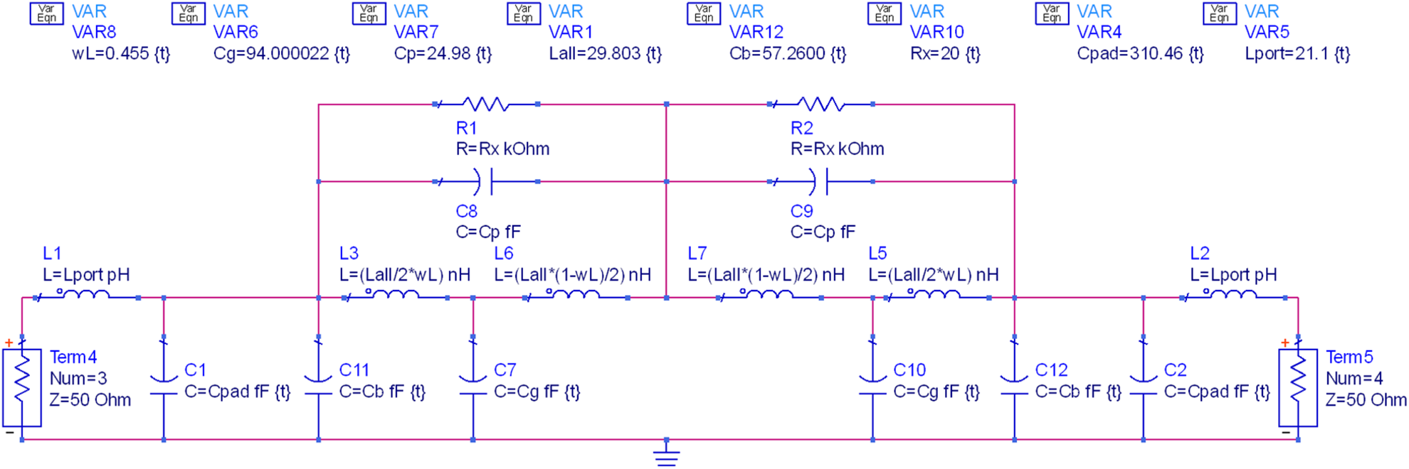
Fig. 10. Discrete equivalent circuit of a single coil. The total inductance of the coil is given by Lall whereas the parameter wL acts as weighting to move the inductance to the symmetry plane (wL = 0) of the circuit or away from the plane (wL = 1).
Figure 11 presents the comparison between 3D EM simulation and the equivalent circuit diagram of one coil. The curves show the absolute values of Z 11 and Z 12 in a logarithmic plot. Note that Z 11 = Z 22 and Z 12 = Z 21 holds on account of the symmetry and of the reciprocity of the structure. Both curves show a good agreement.

Fig. 11. Comparison of the impedance parameters of the 3D EM simulated coil (blue) and the corresponding equivalent circuit diagram (red). Both curves show a reasonable agreement over the entire frequency interval.
Both, the discrete equivalent model for a single coil (refer to Fig. 10) and the model for two coupled coils (not shown) are embedded into a complete circuit model of the outphasing PA.
First, the coil models are combined with the used capacitors (C filt, C DC-block) to simulate the S-parameters and input impedance characteristics of the real outphasing output network (cp. Fig. 2) alone. Figure 12 shows the simulated network including port definitions.

Fig. 12. Simulated outphasing output network including port definitions (1, 2).
As already mentioned material losses are not considered in the CST model. On account of the skin effect, the material losses are frequency dependent. However, we modelled the losses with a constant resistivity of 0.3 Ω. This constant value is a mean value for the frequency-dependent resistivity in the considered frequency range and is therefore considered to be a good compromise. Figure 13 shows the simulated input reflection coefficients (S 11/22) and input impedance characteristic (Z 11/22) from 0 to 4 GHz.

Fig. 13. Simulated input reflection coefficients (top) and input impedance characteristic (bottom) for outphasing output network between 0 … 4 GHz using the extracted model for output network coils from EM simulation; reference impedances at ports 1/2: 64 Ω.
One clearly observes the best matching in terms of input reflection coefficient from the S-parameters in the 800 MHz range, i.e., the clock frequency band chosen for the measurements (see next section). The reference impedance at the input ports is set to 64 Ω. This represents the optimum input impedance Z opt for the used GaN-HEMTs in the FS for a maximum drain supply voltage V DD_max of 60 V and a maximum drain current ID _max of 0.6 A. As the outphasing PA branches are excited in even-mode one must take care of the even-mode impedance Zeven which should be half the value of Zopt, i.e., around 32 Ω. This is in contrast to the odd-mode which has to be suppressed by comparable high impedance (Zodd >> Zopt). The Zopt for the used FS devices with VDD _max and ID _max is calculated as follows:

The output voltage amplitude for the push-pull FS configuration (voltage-mode) used in the DOPA is the fundamental component of a square-wave shaped output signal with ±VDD _max/2. The output current is sinusoidal with maximum amplitude ID _max. The voltage at the series output resonator with a certain load resistance RL is the spectral content of the pulse sequence at (ideally only) the signal frequency according to the modulation used. Therefore we introduce the factor kmod, which refers to amplitudes, not powers. The factor kmod denotes the amplitude coding efficiency for the used modulation scheme and is a scaling factor of VDD _max. For example, in terms of a simple PWM rectangular signal with 50% duty-cycle kmod is equal to 4/π, which represents the prefactor of the first component of the Fourier series.
In Fig. 13 (top) both input reflection coefficients differ due to the additional Laux – CDC -block network at port number 2 (cp. Fig. 12). This is required to support resonant commutation (cp. the section “FS Topology”). In branch 1 (S 11) the input matching is better than 11 dB whereas in branch 2 (S 22) the input matching is only around 7 dB. This translates also in different impedance characteristics (Fig. 13, bottom). The input impedances at 800 MHz show values of 59 Ω at port 1 and 65 Ω at port 2, respectively. The appropriate even-mode impedance Zeven is 24 Ω. Simulated Zodd is sufficiently high with 271 Ω.
Ideally one should provide Zopt at the clock frequency to the FS while very high impedances need to be realized out of band. In both characteristics in Fig. 13 one observes very low impedance around 200 to 300 MHz. This arises due to the unbalance introduced by the additional ReCo support circuit (Laux – CDC -block) at port 2. It may influence performance as spectral components in this region are not properly reflected back into the outphasing circuit. Moreover, the simulated input impedance for branch 1 is too low compared to Zopt (64 Ω). This means that the FS transistors will reach too early, i.e., at a lower drain supply voltage, the current saturation region and thus cannot reach the ideal operation area (VDD _max, ID _max).
To have a preview we simulated the entire outphasing circuit with the coil models in the output stage. For example, at full-scale input, the PA reached a simulated maximum output power of 5.7 W at 30 V drain supply with a total efficiency of 60%. Mean drain current through FSs was 286 mA, which means that current peaks close to ID _max of 600 mA may arise. At 10 dB PBO the efficiency drops down to 25%. From simulation one can derive that due to the lower input impedance as well as Zeven provided by the output network to the FS devices an efficient operating area in terms of maximum current is around 30 V only.
Measurements
All measurements were carried out using an 800 MHz single-tone pulse-width modulated (PWM) input signal. For outphasing operation the phase between the amplifier branches was varied and additionally, the duty cycles for each FS transistor were adjusted, covering the range from 45% for maximum output power Pout down to 25% for high PBO.
Figure 14 presents the simulated and measured results for overall efficiency ηtot as well as for simulated FS drain efficiency ηdrain as a function of PBO at a supply voltage VDD of 30 V. The overall efficiency ηtot includes final stages and drivers, i.e., the full circuit shown in Fig. 2. Again, we must emphasize that the analog (class-A) preamplifiers required to generate the 5 Vpp input voltage swing for the GaN-HEMTs in the outphasing PA to fully switch on and off are not included in the total efficiency calculation (see Section “Driver Circuits”).

Fig. 14. Measured and simulated overall efficiency ηtot as well as simulated final-stage drain efficiency ηdrain vs. power back-off; fclock = 800 MHz, Vdd = 30 V.
The FS drain efficiency ηdrain takes into account the final stage only. Hence, ηdrain cannot be measured directly because a part of the FS current flows into the high-side driver. As shown in Figs 2 and 5 (right) the drains of V2H and V3H are connected to the adjacent CT node, so that the final stage output feeds the positive rail of the high-side driver. Therefore, ηdrain can be obtained only for simulations when one has access to all currents and voltages within the circuit.
From the ηtot characteristics (simulation and measurement) in Fig. 14 one clearly observes that the simulation using the EM simulation-based model of the coils matches the measured circuit quite well, particularly for maximum output power (0 dB PBO) and 10 dB back-off. A maximum difference of 6 percentage points (at 3 dB PBO) has been achieved between simulation and measurement. Considering this the simulated FS drain efficiency values given in Fig. 14 can be considered as realistic as well. This is important since they cannot be measured as stated before.
At the maximum output power of 5.8 W, overall efficiency ηtot reaches 59% and decreases down to 25% at 10 dB PBO. The simulated FS drain efficiency peaks at 71% (0 dB PBO), drops down to 62% at 7 dB, and reaches 67% at 10 dB PBO. Moreover, the final stage efficiency stays above 50% even down to 15 dB PBO. The ηtot curve shows the potential of the digital outphasing approach presented here. In terms of dynamic range, we reached output powers below 1 mW. This means the DOPA reaches at least a dynamic range of 40 dB.
But we have to state that the total efficiency drop with increased PBO is not satisfying since the simulated FS drain efficiency shows an almost constant behavior. Possible reasons for that are discussed in the following.
Discussion of measurement results
Although the simulated and measured total efficiency characteristics match very well one has non-negligible deviations between ηtot and ηdrain, which grow with increasing PBO (25% compared to 67% at 10 dB PBO, for instance). This difference can be attributed on one hand to the FS drivers. While power consumption of the low-side drivers is moderate with 282–359 mW, the high-side drivers take 635–861 mW, of which 326–396 mW are contributed by the negative voltage supply and the pre-drivers plus 353–502 mW (simulated value) by the FS since the positive supply of the high-side driver is connected to the CT voltage, see Fig. 2. Driver power consumption varies only slightly with output power. Therefore, its influence increases with growing PBO.
A second drawback is that the gate-source voltage of the high-side FS transistors cannot reach positive values. While the used FBH GaN technology provides more than 50 V supply voltage – with equivalent higher currents – even at 30 V voltage drops while CT-node is high with about 7 V for amplifier branch A and 4 V for B, shown in Fig. 3(b) (upper). While upper and lower FS transistor has the same size, voltage drop during downslope is significantly lower.
On the other hand, the input impedance characteristic of the output network can have a significant impact. As shown in the section “3D EM Simulation of Output Inductors”, the realized network using EM simulated models for the coils provides even-mode impedance Zeven of 24 Ω at the clock frequency of 800 MHz to the FS transistors. As the optimum (calculated) Zeven is around 32 Ω at fclock a higher output power for a given supply voltage is achieved. This means also a higher current through the FS GaN-HEMTs. Thus, the transistors operate earlier in the saturation region. They cannot reach the maximum simulated drain supply voltage of about 60 V without the risk of damage due to current saturation. This may also influence the PBO behavior of the circuit and represents one reason for the remarkable efficiency drop beyond 10 dB PBO.
Moreover, when assessing the overall efficiency one should take into account that the module has a voltage gain of 16 dB for full-scale, which is higher than for most of the analog outphasing and Doherty solutions, which suffer from relatively low gain.
Conclusion
A very compact digital outphasing PA module including two GaN PA MMICs and a hybrid input/output circuitry for biasing, combining and filtering has been realized for the 800 MHz band. The module reaches a maximum output power of 5.8 W at 30 V FS drain supply voltage, with a gain of 16 dB. The realized PA applies different degrees of resonant commutation (partly or full) for the voltage on the center output nodes, which is optimized for high efficiency in the PBO region. Simulated FS drain efficiency remains between 71 and 67% for a back-off range between 0 and 12 dB, which demonstrates the outphasing functionality and potential. Measured total efficiency reaches 59 and 25% at full-scale and 10 dB PBO, respectively. To identify effects causing the efficiency drop a full 3D EM simulation of the output network inductors has been conducted. Moreover, in order to suppress parasitic effects arising from the module realization advanced techniques like SMD gluing on-chip have been presented.
Future work will focus on further improving efficiency versus back-off and characterizing the module with common broadband modulated signals like Long-Term Evolution (LTE) or Wideband Code Division Multiple Access (WCDMA).
The results achieved so far are already very promising and make the proposed digital outphasing configuration a suitable candidate for future digital transmitter architectures dealing with high PAPR signals.
Acknowledgement
The authors would like to thank Lars Schellhase for the critical assembly of the module, particularly mounting of capacitors with case size 008004 on the MMIC.
Financial support
This work was partly funded by the German Federal Ministry of Education and Research (BMBF) under the project reference 16FMD02 (Forschungsfabrik Mikroelektronik Deutschland).
 Thomas Hoffmann received the diploma from the Technical University of Dresden, Germany. Since 1983 he worked as designing engineer in the research institute “Zentrum für Wissenschaftlichen Gerätebau”, in several companies and as freelancer. There he developed electronic components and devices for industrial use, particularly switch-mode converters. Since 2008, he has been working for the Ferdinand-Braun-Institut (FBH) at Berlin, Germany as a research assistant, where he is developing drivers for pulse laser systems and, since 2015, digital power amplifiers.
 Andreas Wentzel received the Diploma and the Doctoral degree in electrical engineering from the Technical University of Berlin, Germany, in 2006 and 2011, respectively. Since 2015 he has been the head of the Digital PA Lab in the III-V-Electronics department of the Ferdinand-Braun-Institut in Berlin, Germany. His research activities focus on the design, realization, and measurements of flexible digital TX architectures including advanced switch-mode power amplifier concepts realized on GaN and InP from GHz to sub-THz as well as on optimized modulation schemes and filter structures suitable for this type of PAs. Dr. Wentzel is a member of IEEE and MTT society.
 Thomas Flisgen received the Diploma degree in electrical engineering from Hochschule Niederrhein in 2007, the Master and the Doctoral degree in Computational Engineering from University of Rostock in 2009 and 2015, respectively. Since 2018 he is the head of the simulation group of the Ferdinand-Braun-Institut in Berlin, Germany. His main research interests are numerical modeling and simulation of electromagnetic phenomena.
 Florian Hühn received his Dipl.-Ing. in Electrical Engineering from the University of Bremen in 2011. He is currently a Ph.D. candidate in the microwave department of FBH and his research activities focus on modulators for highly efficient switch mode RF power amplifiers and digital microwave PA design.
 Wolfgang Heinrich received the Diploma, Ph.D., and Habilitation degrees in 1982, 1987, and 1992, respectively, all from the Technical University of Darmstadt, Darmstadt, Germany.
Since 1993, he has been with the Ferdinand-Braun-Institut (FBH) at Berlin, Germany, where he is the Head of the Microwave Department and the Deputy Director of the institute. Since 2008, he has also been Professor with the Technical University of Berlin. He has authored or coauthored more than 350 publications and conference contributions. His present research interests include MMIC design with an emphasis on GaN power amplifiers, mm-wave integrated circuits and packaging, and electromagnetic simulation.
Dr. Heinrich has been serving the microwave community in various functions. He served as Distinguished Microwave Lecturer for the term 2003–2005, as chairman of the German IEEE MTT/AP Chapter from 2002 to 2007, as chair of the MTT-12 Committee on interconnects, packaging, and manufacturing from 2006 through 2008, and as Associate Editor of the IEEE Transactions on MTT from 2008 until 2010. From 2010 through 2018, he was the President of the European Microwave Association (EuMA). He is the recipient of the 2019 EuMA Distinguished Service Award.


