I. INTRODUCTION
The microstrip patch antennas are widely used in compact and portable communication devices because of their small size thin profile configurations, conformity and low cost. However, besides having numerous advantages they suffer from some serious drawbacks such as low gain, smaller bandwidth, poor directionality, etc. Various types of losses responsible for low gain of patch antennas are: conductor loss, dielectric loss, and the loss due to excitation of surface waves. The dielectric loss depends on the quality of substrate material its loss tangent, operating frequency as well as dimension of the substrate. Surface wave loss depends on permittivity of the material and substrate's thickness [Reference Waterhouse1]. Several methods have been proposed to reduce losses (conductor and dielectric losses) in patch antennas such as use of good conductor for metallic parts and good dielectric for substrate, etc. Surface wave losses can be reduced by making the designs on the principle that a ring of magnetic current in the substrate having a critical radius, such that they excite very little surface waves [Reference Whittow2]. Another method is to reduce the dielectric value of the substrate, i.e. to replace the substrate of the patch by air or with very low dielectric constant material, known as suspended patch antennas [Reference Chen and Chia3]. An air gap is required for the suspended patch and this is formed by a spacing material such as foam or for fabrication purpose the patch being supported by the posts [Reference Cella, Orten and Hjelmstad4]. The above two methods being fragile are not very durable for mass production and their drawback has been replaced by the electromagnetic band gap (EBG) structures [Reference Sievenpiper5–Reference Llombart7]. The other way to reduce the surface wave loss is by drilling holes in the substrate and hence synthesizing a lower value dielectric substrate [Reference Yoon8, Reference Kildal, Alfonso and Chen9]. The concept of synthesizing a substrate having a lower value of dielectric substrate by removing the substrate partially surrounding the patch is more feasible from the fabrication point of view. The method is to make trenches which are quite narrow, but these methods have not been studied in more detail [Reference Whittow2, Reference Yeap and Chen10–Reference Chen12]. To overcome the drawbacks of the above mentioned technique the method proposed was to partially remove the substrate to reduce the surface wave losses [Reference Rao and Vishwakarma13]. The other way is to use drilled hole EBG structure [Reference Rao and Vishwakarma14] or mushroom-type EBG as substrate [Reference Liang and Yang15, Reference Ruaro, Thaysen and Jakobsen16]. EBG structures are periodic structures, which stop the propagation of wave in a particular band of frequency for all incident angles. If the resonant frequency of the antenna lies in the band gap, then the patch with EBG structure shows an enhancement in the gain of antenna due to suppression of surface wave.
The paper reports a novel mushroom-type EBG structure, consisting of fractal periodic elements. The proposed fractal EBG is found to suppress surface waves more effectively, thus resulting in higher gain when used as substrate for the patch antennas. A comparative study of circular mushroom EBG with sierpinski fractal-shaped EBG has been carried out. The implementation of fractal EBG has enhanced the gain of patch antennas significantly as compared with circular mushroom EBG for wireless communication at 6 GHz.
All simulations have been carried out using CST Microwave studio which is a comprehensive tool for electromagnetic analysis based on the finite integration technique. Before performing simulation of proposed structures, the results of published paper “Wearable dual-band Sierpinski fractal PIFA using conductive fabric” [Reference Soh17] were verified. The calculation shows bandwidth of antennas 339.3 and 64 MHz at frequencies 2.29 and 4.8 GHz which are in close agreement with the published results: 345 and 615 MHz at 2.45 and 5.2 GHz. The radiation patterns are also in close agreement, these validate our simulation procedure.
II. FRACTAL EBG DESIGN
This section describes the design of fractal EBG structure which enhances the gain of patch antenna more than the mushroom-type EBG. Fractal shapes are those in which there is repetition of a particular shape which is scaled up or scaled down. Figure 1 shows the unit cell of circular and sierpinski fractal-shaped mushroom EBG [Reference Ullah and Islam18, Reference Quarfoth and Sievenpiper19]. The sierpinski fractal is made by adding the scaled down triangles to each edge of the existing triangle as shown in Fig. 2.

Fig. 1. Two designs of mushroom EBG.

Fig. 2. Fractalization process upto fourth iteration.
A) Triangular fractal
The dimension of the triangular-shaped fractal is 7.20 mm in length and 7.20 mm in altitude over all. Sierpinski fractal is made adding the scaled down triangles to each edge of the previous triangles. The scaling factor of the fractal is k = 0.50 for length and altitude of the triangular geometry. The dimensions are given by equations (1) and (2). In the equations ‘i’ represents the iteration number. The subsequent lengths and altitudes are calculated and added to make it a fractal-shaped EBG as shown in Figs 2(a)–2(d). The gap between the two adjacent triangular fractal mushroom EBG is 1.20 mm. The periodicity of the fractal-shaped mushroom EBG is 8.40 mm, formed on a substrate of height 1.54 mm with dielectric constant ε r = 4.3 (Rogers R04003). The elements of the EBG structures are shorted to ground plane via shorting pins. The dispersion diagram is shown in Fig. 3. The EBG with square matrix has a band gap in frequency range 5.8–6.5 GHz.
 $${L_{i+1}}={k^i} \times {L_i}\comma \;$$
 $${H_{i+1}}={k^i} \times {H_i}.$$

Fig. 3. (a) Dispersion diagram of the circular-shaped mushroom EBG. (b) Dispersion diagram of the Sierpinski fractal mushroom EBG having band gap between 5.8 and 6.5 GHz.
III. PATCH ANTENNA DESIGN
This section describes the design of patch antennas on the dielectric substrate (Rogers R04003) as well as on the mushroom EBG substrate with and without fractals.
A) Patch on normal substrate
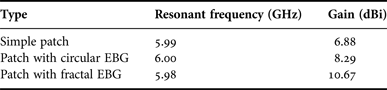
The rectangular patch has been placed on the substrate with a ground plane at the bottom as shown in Fig. 4(a). The dimension is 15.78 mm × 13.00 mm of the patch printed on a substrate of dimension 85.62 mm × 85.62 × 1.54 mm having dielectric constant of ε r = 4.3 with a ground plane at the bottom. The patch is fed by a microstrip line. Simulation shows that the rectangular patch is resonant at a frequency of 5.99 GHz having bandwidth nearly 100 MHz and S 11 is −29.50 dB.

Fig. 4. Different configurations for the patch and EBG. (a) Conventional rectangular patch. (b) The conventional patch with circular mushroom EBG. (c) The conventional patch with fractal-shaped mushroom EBG (sierpinski fractal).
B) Patch on EBG substrate
Mushroom-type EBGs have been incorporated for the patch antenna as shown in Fig. 4(b). For the circular-shaped mushroom EBG, the diameter is 6.00 mm and periodicity 7.00 mm. The square matrix is formed on the dielectric substrate, with 3 × 3 elements missing from the center of the array to accommodate the antenna patch as shown in Fig. 4(b).
C) Patch on fractal-shaped EBG
The triangular elements of the mushroom EBGs are fractalized resulting in fractal mushroom EBGs. The fractalization process for the first four iterations has been shown in Fig. 2. The properties of the antennas have been investigated on fractal EBGs and the results of return loss, far field's polar and three-dimensional (3D) plots have been shown in Figs 5–8, respectively.

Fig. 5. S 11 of rectangular patch, rectangular patch with circular-shaped mushroom EBG and rectangular patch with fractal-shaped mushroom EBG.

Fig. 6. Radiation pattern for the different configurations. (a) The E-plane radiation pattern for rectangular patch, rectangular patch with circular-shaped EBG and rectangular patch with fractal-shaped mushroom EBG. (b) The H-plane radiation pattern for rectangular patch, rectangular patch with circular-shaped EBG and rectangular patch with fractal-shaped mushroom EBG.

Fig. 7. The LC modeling of mushroom EBG.

Fig. 8. Three-dimensional radiation pattern for optimized results. (a) Three-dimensional radiation pattern for the rectangular patch. (b) Three-dimensional radiation pattern for the rectangular patch with circular-shaped mushroom EBG. (c) Three-dimensional radiation pattern for the rectangular patch with fractal mushroom EBG.
The triangular-shaped EBG has been fractalized up to fourth iteration because for the fourth iteration the band gap of the fractal and circular-shaped mushroom EBGs are same.
IV. RESULTS AND DISCUSSION
The mushroom EBG structures are artificial magnetic conductors. The impedance between the two successive elements is calculated using an L–C modeling of the EBG [Reference Ullah and Islam18]. The edge of the mushroom patch results in the generation of capacitance between the two elements and the shorting pin contributes for the inductive part. As a result the impedance offered by one pair of mushroom structures is given by:
 $${Z_0}=\displaystyle{{j\omega L} \over {1 - {\omega ^2}LC}}.$$
The capacitance between the two edges depends on the length of the edge; by the process of fractalization the length of the edge has been increased. Increase in the number of corners increases the capacitive behavior between the two elements. As a result the denominator decreases which increases the overall value of Z 0 of equation (3) so the suppression of surface wave takes place more efficiently. Since the increase in the capacitance cannot be measured numerically. This paper shows a comparative study of the EBG from no corners (circular-shaped mushroom EBG) to the sierpinski fractal with increased number of corners.
The conventional mushroom EBG suppresses the surface wave in a particular direction. Surface wave passing through the fractal-shaped mushroom EBG are scattered in all the direction and scattering takes place because of the irregularity in the shape of the patch of mushroom EBG. The scattered surface waves are more effectively suppressed in all the directions by the fractal-shaped mushroom EBG. The polar plots of far fields in the E- and H-planes for different configurations of the antennas have been shown in Fig. 6. The results are summarized in Table 1 and Fig. 8 shows 3D radiation patterns of antennas on circular as well as fractal EBG substrate.
Table 1. Gain and resonant frequency comparison for different EBG configurations

It is thus clear that as compared with conventional type EBG, fractal EBGs proposed and designed in the present study are more effective in suppressing surface waves resulting in higher gain and of patch antennas. This investigation will be very useful in performance enhancement of patch antennas as well as other high-frequency planar circuits requiring EBG substrate materials.
V. CONCLUSION
New mushroom-type EBG structures consisting of fractalized periodic elements have been proposed and used as substrate for microstrip patch antennas. It is found that the proposed fractal EBGs suppress surface waves resulting in larger gain enhancement of the antennas and better directionality as compared with conventional mushroom-type EBGs. The gain of patch antennas has almost doubled with fractal EBG structures as compared with normal substrate. The proposed fractal EBG will open new avenues for the design and development of variety of high-frequency components and devices with enhanced performance.
 Neeraj Rao received the Bachelor of Technology (B. Tech.) degree in Electronics and Communication Engineering from Government Engineering College, Jabalpur, India, and the Master of Technology (M.Tech.) degree in Electronics and Communication from Indian Institute of Information Technology Design and Manufacturing Jabalpur, India. He is currently pursuing the Ph.D. degree in the Department of Electronics and Communication Engineering from Indian Institute of Information Technology Design and Manufacturing Jabalpur, India. His research areas include Microstrip Patch Antennas, Fractal Antennas.
 Dr. Dinesh Kumar Vishwakarma received his Ph.D. in Electrical Communication Engineering from Indian Institute of Science, Bangalore in 2005. Post Doctoral Research in Japan, National Institute for Material Sciences (NIMS), Tsukuba, Nov. 2006–July 2009. He became an Assistant Professor in IIIT DM Jabalpur in 2009. He is currently serving as an Associate Professor in IIIT DM Jabalpur.