


I. INTRODUCTION
Ultra wideband (UWB) communication system has become more popular among researchers and the wireless industries after the permission of Federal Communication Commission (FCC) in 2002 for its commercial usage within the frequency range from 3.1 to 10.6 GHz [1]. Several shapes of monopole antenna geometry have been designed so far to cover the entire bandwidth of UWB including different types of patch structure or modification of ground plane or embedding parasitic elements, etc. [Reference Zaker and Abdipour2–Reference Li, Zhai, Li, Ma and Liang4]. In recent years the main challenge is to design UWB antenna with band notch characteristics to avoid electromagnetic (EM) interference on the other wireless narrowband systems such as world interoperability for microwave access (WIMAX) (3.3–3.7 GHz) and wireless local area network (WLAN) (5.15–5.825 GHz). The conventional techniques of band rejection characteristics are mainly based on the implementation of half wavelength or quarter wavelength filter structure in Antenna. Several techniques have already been reported to achieve band stop characteristics by using slot insertion on patch surface or ground plane or to the feed line, insertion of parasitic element around the patch or conductor backed plane (CBP) on the rear side of patch, employing stub to the patch or the ground plane. Previous literatures related to band notched performance of UWB monopole are based on the investigation and optimization of voltage standing wave ratio (VSWR), radiation pattern, peak gain, etc. [Reference Rostamzadeh, Mohamadi, Nourinia, Ghobadi and Ojaroudi5–Reference Samadi Taheri, Hassani and Ali Nezhad11]. However time domain behavior is an important issue which must be considered in the design of band notched UWB antenna. Hence antenna should be designed carefully to avoid undesired distortion and ringing [Reference Yang, Chu and Zheng12–Reference Koohestani, Pires, Skrivervik and Moreira14]. This paper presents a new design of UWB monopole antenna with arrow shaped patch. Symmetrical steps with the lower periphery of the patch and U-shaped ground plane truncation leads to bandwidth enhancement from 2.2 to 12 GHz. In order to generate dual band notched characteristics, symmetrical open ended angularly separated narrow slit pair on the patch surface and angularly separated CBP pair on the other side of patch is inserted. Center frequency of the notched bands corresponding to WIMAX (3.3–3.9 GHz) and WLAN (5.15–6 GHz) bands can be controlled easily and independently by varying the length of the slit pair and CBP pair correspondingly. Angular separation between the slot pair and CBP pair play significant role in band rejection performance. The dual band rejections are mutually uncorrelated because of the placement of slit pairs on the radiator and CBP pair on the other side of the patch. Good time domain characteristics in terms of correlation factor and pulse stretch ratio (SR) establish the employability of the proposed antenna in practical UWB systems.
II. DESIGN OF UWB ANTENNA WITH BAND-NOTCHED CHARACTERISTICS
Geometry of reference antenna without band rejection characteristics is fabricated on a 30 × 30 mm2 FR4 substrate with є r = 4.4 and thickness of 1.58 mm; the ground plane side length L g is 7 mm, W f is fixed at 2 mm to maintain 50 Ω characteristics impedance. By cutting four pairs of rectangular 2 × 2 mm2 sequential steps on the lower side of the arrow shaped patch surface along with the U-shaped truncation to the edge of the ground plane, perfect EM coupling between the radiator and ground plane can be obtained. The optimized dimension of U-shaped slot is 10 × 1.7 mm2. Modified structure provides multiple resonances in higher frequency range resulting bandwidth enhancement by 27% (3.78 GHz) as shown in Fig. 1. Actually the sequential steps at the lower side of the patch provide the balance between vertical and horizontal surface current on the patch, which leads to the additional resonance frequencies. More over U-shaped truncated ground plane acts as an impedance matching element which increases the sensitivity of the higher frequencies [Reference Zaker and Abdipour2]. Therefore by adjusting the dimension of U-shaped truncation on the ground plane, good impedance matching between the radiating patch and the ground plane over a wide frequency band can be achieved.

Fig. 1. Simulated return loss characteristics for reference antenna.
Proposed antenna configuration with band reject elements consists of a pair of open ended thin slit on the patch surface and a pair of rectangular CBP on the opposite side of the patch as shown in Fig. 2. Angular separation between the slit pair α and CBP pair β play significant role regarding band rejection performance but they have insensitive influence to the center frequency of the rejection band. Minimum gap between the slit pair is G S with the length of each slit being L S . On the other hand, each CBP has a length of L P and minimum gap between the CBP pair is G P . Hence rejection frequency for the WIMAX band notched characteristics is empirically approximated as
 $${f_{notch - wimax}} = \displaystyle{c \over {2 \times {L_{n1}} \times \sqrt {{\epsilon _{reff}}}}}, $$
and the rejection frequency for WLAN band notched characteristics is approximated as
 $${f_{notch - WLAN}} = \displaystyle{c \over {2 \times {L_{n2}} \times \sqrt {{\epsilon _{reff}}}}}, $$
where L n1 and L n2 are set to band stop resonate at λ g1/2 and λ g2/2 where λg 1 and λg 2 correspond around the band notch frequency of 3.5 and 5.5 GHz and for this structure L n1 and L n2 are defined as L n1 = 2 × L S + G S , Ln 2 = 2 × L P + G P , effective dielectric constant is є reff = є r + 1/2. The above formulas are validated by comparing simulated results and predicted results by High Frequency Structure Simulator (HFSS). Figure 3(a) shows the different value of open ended slit length keeping fixed value of α = 60° and G S = 2.59 mm. As can be noticed, the nature of slope for both the calculated and the HFSS results are in parity and the results attain minimum difference in between 3.3 and 3.9 GHz. Similarly, Fig. 3(b) shows comparison between simulated and calculated results of the length of CBP against frequency keeping β fixed at 70° and G P = 3.5 mm which exhibits almost similar slope. Slight difference is observed in between calculated and predicted length in both cases because of the approximation adopted in the calculation of effective dielectric constant.

Fig. 2. Geometry of the proposed UWB antenna with dual band notch characteristics. (a) Top view, (b) bottom view.

Fig. 3. Comparison of calculated and predicted length of (a) resonator slit L S and (b) CBP L P corresponding to the notch frequencies.
To verify the geometry, proposed antenna is modeled, simulated, and optimized by using EM simulator HFSS 13. The final dimension of each Antenna parameters of the proposed design is as follows: W sub = 30 mm, L sub = 30 mm, L g = 9 mm, D = 18.6 mm, L f = 9 mm, W f = 2 mm, L 1, L 2, L 3, L 4 = 2 mm, W 1, W 2, W 3, W 4 = 2 mm, G s = 2.81 mm, G p = 4.84 mm L s = 11.34 mm, L p = 15.69 mm, α = 70°, β = 60°
III. RESULTS AND DISCUSSION
A) Parametric analysis of 3.5 and 5.5 GHz notched bands
Figures 4(a) and 4(b) present the return loss performance of rejection frequency band around 3.5 and 5.5 GHz, respectively, due to the individual effect of open ended slit pair and CBP pair. Figure 4(c) presents the combined effect of both notch elements where dual rejection frequency bands around 3.5 and 5.5 GHz. The simulation of frequency domain analysis has been performed by using Ansoft HFSS simulator. Frequency band rejection performance and tuning of the center rejection frequency has been separately investigated for angularly separated open ended slit pair and angularly separated CBP pair as observed in Fig. 5. Figures 5(a) and 5(b) shows the simulated VSWR with different value of L S and L P , When L S changes from 10.12 to 12.43 mm, center frequency of notch band decreases from 4 to 3.3 GHz. Similarly, shifting of L p from 14 to 18 mm shifts the center frequency of notch band from 6.2 to 5.4 GHz. Angular separation α and β control the peak VSWR and notch width of the rejection band. As α reduces, the patch surface between the slit pair becomes narrower which influence the coupling between patch and the ground plane. Therefore worse coupling between patch and the ground plane maximizes the peak VSWR at 3.5 GHz with increment in rejection bandwidth. On the other hand at WLAN frequency band, maximum patch current is concentrated at the lower edge. Therefore if β becomes higher, the direction of the current of the CBP and current at the edge of the patch are exactly opposite to each other resulting high impedance mismatch which increases peak VSWR at 5.5 GHz with increased notched bandwidth as shown in Figs 5(c) and 5(d). In this proposed antenna, slit pair and CBP pair are inserted to realize two targeted resonating frequencies at 3.5 and 5.5 GHz, respectively, so that the coupling effect between them is necessary to be investigated. Figures 6(a) and 6(c) show that when L S and α vary keeping all other parameters constant, there are no effect on WLAN frequency band. Similarly, Figs 6(b) and 6(d) show no effect in WIMAX band while L P and β are varied. Therefore it may be concluded that there is almost negligible coupling effect between the open ended angularly separated slit pair and angularly separated CBP pair.

Fig. 4. Simulated return loss against frequency due to individual band-notched element. (a) Slot pair, (b) CBP pair, and (c) combination of slot and CBP pair.

Fig. 5. Simulated VSWR plot for variation of parameters of individual band notched elements (a) L S (α = 50°), (b) L P (β = 60°), (c) α(L S = 12.43 mm), (d) β(L P = 16 mm).

Fig. 6. Simulated VSWR of the proposed antenna with different values of (a) L S (α = 50°, β = 60°, L P = 16 mm), (b) L P (α = 50°, β = 60°, L S = 12.43 mm), (c) α(L S = 12.43 mm, L P = 16 mm, β = 60°), and (d) β(L S = 12.43 mm, L P = 16 m.m, α = 50°).
B) Experimental verification
To verify the proposed design, a prototype of the antenna based on optimized dimension has been fabricated (as shown in Fig. 7) and measured. The experimental results exhibit the range of impedance bandwidth (VSWR ≤ 2) between 2.2 and 11 GHz with dual notched bands 3.3–3.9 and 5.1–6 GHz as shown in Fig. 8 where a very good agreement between the simulated and measured values is observed.

Fig. 7. Photograph of the fabricated prototype of proposed antenna.

Fig. 8. Measured and simulated VSWR of the proposed antenna.
C) Current distribution analysis
Simulated magnitude and vector current distribution are illustrated in Fig. 9. at the notch frequency of 3.5 GHz. Surface current is mainly concentrated around the slit. Excited surface currents on both side of the slit are oppositely directed and hence they cancel each other. As a result, antenna does not radiate around 3.5 GHz. Similarly surface current at 5.5 GHz is mainly distributed on the edges of the patch surface as well as the CBP pair and they are oppositely directed which causes high attenuation making the antenna nonresponsive at that frequency.

Fig. 9. Simulated magnitude and vector current distribution of proposed antenna at 3.5 and 5.5 GHz.
D) Radiation pattern and antenna gain
Measured far field radiation patterns in YZ-plane (E-plane) and XZ-plane (H-plane) are plotted in Fig. 10 for 7 and 10 GHz. The nature of E-plane patterns are monopole-like and the H-plane patterns are nearly Omnidirectional though distortion can be observed at 10 GHz. Figure 11 illustrates the measured peak gain of proposed antenna against frequency. The peak gain is relatively flat over the entire operating frequency band except a sharp decrease in the vicinity of 3.5 and 5.5 GHz.

Fig. 10. Measured radiation pattern of the proposed antenna.

Fig. 11. Measured peak Gain of the proposed antenna.
IV. TRANSFER FUNCTION AND TIME DOMAIN ANALYSIS
A) Group delay and transmission characteristics
Transfer function and group delay characteristics for face to face and side by side orientation (keeping two identical antennas 30 cm apart) are presented in Fig. 12. Group delay characteristics are almost smooth over the entire UWB band except stop bands where the variation of group delay is greater than 1 ns for each orientation. However in pass band, the group delay less than 1 ns indicates the good linear phase response. Magnitude of the transmission coefficient (|S 21|) has also the sharp dips at the stop bands. Group delay corresponds well to the magnitude of S 21. Therefore it can be concluded that the antenna has small waveform distortion due to the phase nonlinearity.
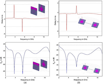
Fig. 12. Magnitude of the transmission coefficient S 21 and group delay of the proposed antenna. (a) Face to Face mode, (b) side by side mode.
B) Waveform response
Satisfactory frequency domain performance does not necessarily ensure the excellent time domain behavior. Therefore, time domain characteristics are vital to the system performance. In this article the system response has been analyzed by CST microwave studio software. Since the UWB antenna is inspired by the transient Gaussian pulse, a modulated Gaussian pulse, as an excitation waveform, has been chosen as given by the mathematical expression p(t) = cos (2πf c t)exp[ − 2π(t/τ)2]. In order to cover the spectral response within the UWB frequency band (referred by FCC), the center frequency f c = 6.85 GHz and Gaussian width τ = 228 ps are considered. For minimum pulse broadening at the receiving end, the pulse preserving capability of the antenna becomes higher, which results in the high rate of data transmission. As the proposed antenna has XZ-plane (H-plane) radiation pattern is almost Omnidirectional. Thus for simplicity, the normalized radiated pulses for different angular value θ in XZ-plane are investigated as shown in Fig. 13. It can be observed that radiated pulse waveforms are distorted as compared with the excited pulse due to the band rejection characteristics of the antenna. Figure 14 illustrates the input Gaussian pulse at the transmitting antenna terminal and the received signals which is obtained by placing a pair of identical antennas in face to face and side by side orientation with a separation of 60 cm and their corresponding normalized frequency spectrums are also plotted. As observed in both face to face and side by side mode, the late time oscillation or ringing effect occur in the received signals and the corresponding spectrum has sharp dip at 3.5 and 5.5 GHz in each mode which confirms the results of VSWR and transfer function. In addition to the impact of the notch, reduction of the spectrum bandwidth can also be seen in both the cases.

Fig. 13. Normalized excitation pulse and radiated signal in XZ-plane with different values of detecting angle θ.

Fig. 14. Comparison of normalized waveform and frequency spectra for (a) excitation pulse, (b) received signal in face to face mode, (c) received signal in side by side mode.
In order to quantify distortion between transmitted and received signals, two figure of merit referring to correlation factor and pulse width SR are introduced.
C) Correlation factor
The correlation factor is defined as
 $\rho = \mathop{max}\limits_{\tau} \left\{ \left\vert (\int v_t (t) v_r (t - \tau) dt)/ \sqrt{\int v_t^2 (t) dt} \sqrt{\int v_r^2 (t) dt} \right\vert \right\} $
where v
t
(t) = transmitted signal, v
r
(t) = radiated electric field intensity or receiving antenna signal at far field region, and τ = time delay [Reference Peng and Ruan13]. Maximum value of correlation factor is unity when two signals are identical but it is reduced when received signal is the attenuated or delayed version of transmitted one. To determine the correlation factor of radiated electric field signals and the receiving antenna signals, the radiated signal in XZ-plane at θ = 0° is depicted as the reference signal waveform similar to the transmitted signal v
t
(t). Table 1 presents the correlation factor of v
t
(t) and far field radiated intensity signals obtained by different probe location or received signal in face to face and side by side mode (considered as v
r
(t)). As observed from Figs 13, 14, and Table 1, ringing duration is highest for minimum value of correlation factor in face to face mode.
$\rho = \mathop{max}\limits_{\tau} \left\{ \left\vert (\int v_t (t) v_r (t - \tau) dt)/ \sqrt{\int v_t^2 (t) dt} \sqrt{\int v_r^2 (t) dt} \right\vert \right\} $
where v
t
(t) = transmitted signal, v
r
(t) = radiated electric field intensity or receiving antenna signal at far field region, and τ = time delay [Reference Peng and Ruan13]. Maximum value of correlation factor is unity when two signals are identical but it is reduced when received signal is the attenuated or delayed version of transmitted one. To determine the correlation factor of radiated electric field signals and the receiving antenna signals, the radiated signal in XZ-plane at θ = 0° is depicted as the reference signal waveform similar to the transmitted signal v
t
(t). Table 1 presents the correlation factor of v
t
(t) and far field radiated intensity signals obtained by different probe location or received signal in face to face and side by side mode (considered as v
r
(t)). As observed from Figs 13, 14, and Table 1, ringing duration is highest for minimum value of correlation factor in face to face mode.
Table 1. Correlation factors of the proposed antenna.

D) Pulse width SR
SR has significant role to analyze pulse preserving capability of UWB antenna. SR is defined as the ratio of the width of the received waveform v r (t) to the width of the transmitted waveform v t (t).For the 90% captured energy between v t (t) and v r (t),the SR is defined as [Reference Peng and Ruan13]
 $$SR = \displaystyle{{{{\left[ {\mathop \int \nolimits_{ - \infty} ^{ + \infty} \vert {V_r}(t){ \vert ^2}dt} \right]}^{ - 1}}(0.95) - {{\left[ {\mathop \int \nolimits_{ - \infty} ^{ + \infty} \vert {V_r}(t){ \vert ^2}dt} \right]}^{ - 1}}(0.05)} \over {{{\left[ {\mathop \int \nolimits_{ - \infty} ^{ + \infty} \vert {V_t}(t){ \vert ^2}dt} \right]}^{ - 1}}(0.95) - {{\left[ {\mathop \int \nolimits_{ - \infty} ^{ + \infty} \vert {V_t}(t){ \vert ^2}dt} \right]}^{ - 1}}(0.05)}}$$
Minimum value of the pulse width SR is unity which increases with increasing value of the ringing duration. SR is calculated in the XZ-plane for the electric field intensity for different detecting angles where maximum value at θ = 90 is observed. SR value for receiving antenna in face to face and side by side mode are 2.45 and 1.83, respectively, as shown in Table 2. Hence side by side orientation is preferable over face to face orientation. Correlation factor and SR clearly indicate the effect of small ringing distortion owing to the impedance mismatch at the rejection bands.
Table 2. The pulse width SR values for the proposed antenna.

V. CONCLUSION
In this work, a compact UWB antenna with dual band notch function is presented and investigated. The design methodology is the utilization of an arrow shaped patch with multiple symmetrical steps to obtain UWB property. A new approach is introduced for dual band stop characteristics around 3.3–3.9 and 5.1–6 GHz with UWB antenna by incorporating the open ended slit pair on the radiator and CBP pair on the rear side of the radiator. Angular separation between the slit pair and CBP pair is crucial for enhanced band rejection. Proposed antenna has demonstrated satisfactory performance in terms of VSWR, gain, radiation pattern, current distribution, and transfer function. The extensive investigation has also been carried out to extract the time domain characteristics of the proposed antenna. With minor interference among WIMAX and WLAN, the proposed antenna is expected to be a good candidate for the UWB application.
ACKNOWLEDGEMENT
The author expresses their sincere gratitude to the Department of Engineering and Technological Studies, University of Kalyani, Kalyani, West Bengal, India.
 Rajarshi Sanyal has obtained his AMIETE and M.Tech. degree in Electronics and Communication. His area of Research includes Micro strip Antenna and Micro strip filters. Presently he is associated with MCKV institute of Engineering as an Assistant Professor. He has presented and published various research papers in national and international journals.
 Abhirup Patra obtained his B.Tech. degree in ECE from Calcutta Institute of Technology 2013 and is pursuing M.Tech. in E.C.E from MCKV IE both under WBUT. His primary research interest includes DSP, Micro-strip Antenna, and Microwave solid state devices.
 Prof. (Dr.) P. P. Sarkar obtained his M.E. and Ph.D. in Engineering from Jadavpur University in the year 1994 and 2002, respectively. He earned his B.E degree in Electronics and Telecommunication Engineering from Bengal Engineering College (presently known as IIEST, Shibpur) in the year 1991. He is presently working as Professor at the Dept. of Engineering & Technological Studies, University of Kalyani. His area of research includes, Microstrip Antenna, Microstrip Filter, Frequency Selective Surfaces, and Artificial Neural Network. He has contributed to numerous research articles in various journals and conferences of repute. He is also a life Fellow of IETE (India) and IE (India).
 Prof. (Dr.) Santosh K.R. Chowdhury obtained his M.E. and Ph.D. in Engineering from Jadavpur University in the year 1968 and 1971, respectively. He earned his B.E degree in Electronics and Telecommunication Engineering from Jadavpur University in the year 1964. He is a Senior Member of IEEE, Life fellow of IETE, Fellow of IE, Fellow of West Bengal Academy of Science and Technology. His area of research includes, Microstrip Antenna, Microstrip Filter, and Frequency Selective Surfaces. He has contributed more than 50 international research articles in various journals and conferences of repute.


