I. INTRODUCTION
Power dividers (PDs) and combiners, as key passive components, have been widely applied in various microwave and millimeter-wave systems such as mixers, power amplifiers, and phase-array antennas [Reference Pozar1]. Among all kinds of in-phase PDs, Wilkinson and Gysel PDs (GPD) are the most commonly used ones [Reference Wilkinson2–Reference Wang, Wu and Yin7]. Although the Wilkinson PD has many advantages such as reasonable bandwidth, simple layout, and good isolation between output ports, it is not applicable for high-power applications due to the internal isolation resistor, which is not connected to the ground plane.
Compared with the Wilkinson PD, the GPD with external grounded isolation resistors, allows good power-handling performance for high-power applications [Reference Gysel5], in that it has two resistors while both of them are connected to the ground plane. In addition, it is possible to put resistors out of the structure using a suitable transmission line (TL) connected to the resistors. Therefore, the heat-sinking procedure can be done more properly.
Similar to Wilkinson PD, GPD is an N-way divider and the drawback of both of them is that, they require a central node to which all ports are connected. Hence, it may be difficult to realize an N-way divider at high frequencies and add especially for the large N. Moreover, when the output ports are more than two, the realization of the PD, which is planar, is not simple. Therefore, a useful method for ease of fabrication of the N-way GPD has been presented in [Reference Beyragh, Abnavi and Motahari8].
On the other hand, with the rapid development of modern wireless communication systems, dual-band or frequency reconfigurable components are in increasing demand. Thus, many dual-band GPDs with equal [Reference Ren, Fan, Zhu and Hu9–Reference Zhang, Wu, Nan, Wang, Su and Liu11] or unequal power divisions [Reference Sun, Zhang, Yan and Yang12–Reference Hayati, Malakooti, Jamshidi and Yari Sarvarani15] have been reported in the past few years. It is worth noting that the number of output ports of these dual-band GPDs are only limited to two. In other words, to the best of the authors’ knowledge, multi-way dual-band GPDs have not been taken into consideration.
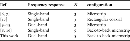
Moreover, Table 1 summarizes the performance of some of the most important GPDs. They are categorized according to the number of ports and their frequency functions for convenient comparison. It can be seen that all of dual-band GPDs [Reference Ren, Fan, Zhu and Hu9–Reference Hayati, Malakooti, Jamshidi and Yari Sarvarani15] are only three port dividers while five port Gysels [Reference Beyragh, Abnavi and Motahari8, Reference Fan, Liang, Geng and Jin16] are limited to one band of operation.
Table 1. Summary of the GPDs according to the number of ports and frequency responses.
In this study, a four-way dual-band GPD is designed and fabricated. It is clearly seen that the proposed GPD can be very important and necessary in some applications. In order to make a planar structure, the back-to-back method used in [Reference Beyragh, Abnavi and Motahari8] is applied. In addition, the dual-band response is realized by adding an open-circuit stub and a short-circuit stub to the structure of the PD. In fact, the main characteristics of the proposed PD include: (1) dual-band, (2) four-way, (3) exact closed-form design method, and (4) high power-handling capability.
II. DESIGN PROCEDURE
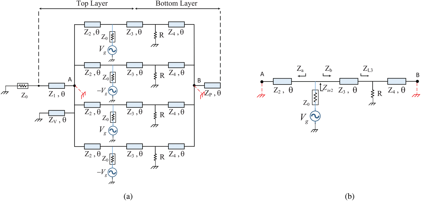
Figure 1 depicts the proposed four-way PD for dual-band applications. In addition, the characteristic impedances and electrical lengths of each arm of the PD are shown in this figure. It can be observed that the five-port structure consists of four TLs (Z 1, Z 2, Z 3, Z 4), a short-circuit stub (Z v), an open-circuit terminated stub (Z p), as well as four isolation resistors (R), while the termination resistance is Z °. Moreover, the corresponding electrical length of all TLs is θ.
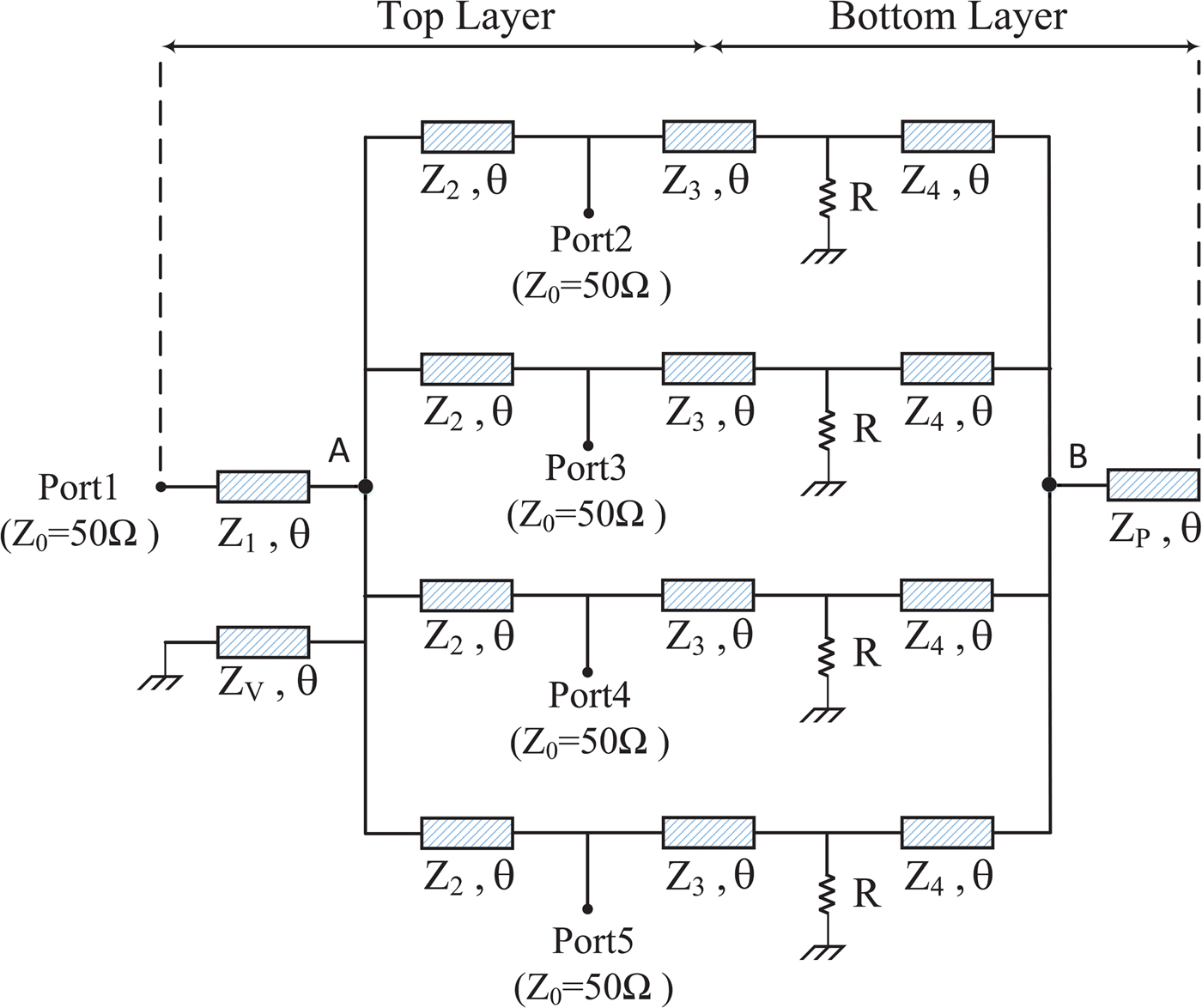
Fig. 1. Schematic diagram of the proposed GPD.
The proposed in-phase PDs satisfy the following conditions at the center of its operating frequency:
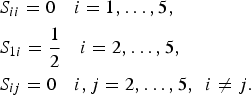 $$\eqalign{& S_{ii} = 0\quad i = 1, \ldots, 5, \cr & S_{1i} = \displaystyle{1 \over 2}\quad i = 2, \ldots, 5, \cr & S_{ij} = 0\quad i,j = 2, \ldots, 5,\,\,\,i \ne j.} $$
These conditions imply that the input power is divided equally among the four outputs and an impedance matching is seen from each port. Hence, we call them the conditions for equal ideal power transmission.
In order to get the generalized analytical method to design the PD structure, the conditions (1) alongside the circuit TL theory are applied. For this purpose, first, only port 1 is excited. By applying the conditions for ideal power transmission, relationships between some characteristic impedance values are derived, which are described in more details in Section II.A. Then, in Section II.B, ports 2 , 3, 4, and 5 are excited. It is worth noting that in order to simplify the analyse procedure, the voltage sources at ports 2 and 4 are assumed to be V g, while the voltage sources at ports 3 and 5 are considered −V g. Again using the conditions for ideal power transmission, which define constraint rules for the design of PD, and the principle of superposition the relationships between other characteristic impedance values are achieved. Finally, the design of PD is finished when all equations are solved and the value of each characteristic impedance is defined.
A) Excitation of port 1
As shown in Fig. 2(a) at this stage, it is assumed that only port 1 is excited. According to the above discussions, the PD is designed so that all of the input power is transformed to output ports equally. Therefore, not only no power is dissipated in the isolation resistors, but also a matched condition should be seen at port 1. Figure 2(b) shows the simplified equivalent circuit under these constraint rules. Since no power is transferred in the isolation resistors, it can be seen that they are shorted in the equivalent circuit.
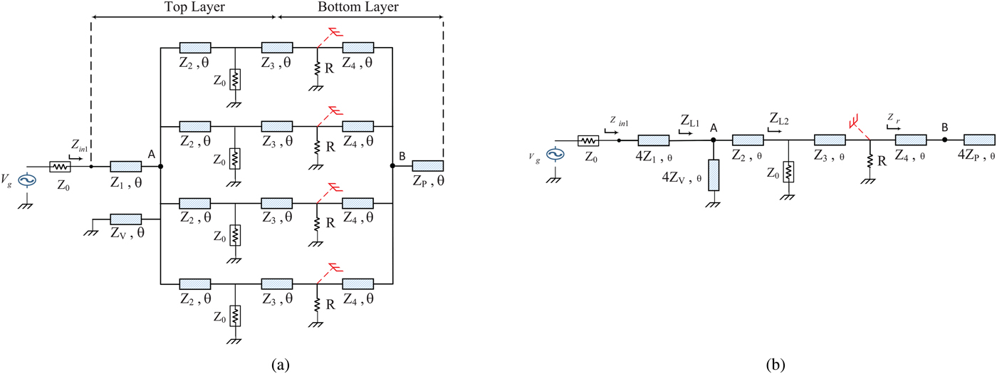
Fig. 2. (a) Excitation of port 1. (b) Simplified equivalent circuit.
Moreover, to satisfy the matching condition at port 1, it is expected that the impedance seen at this port be equal to 4Z °, namely, Z in1 = 4Z °. Then, by normalizing all of the impedance values to Z °, the input impedance at port 1 can be expressed as
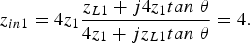 $$z_{in1} = 4z_1\displaystyle{{z_{L1} + j4z_1tan\; \theta} \over {4z_1 + jz_{L1}tan\; \theta}} = 4. $$
The impedance values in lowercase indicate that they are normalized to Z °. In equation (2), we have
 $$z_{L1} = \displaystyle{{ - 4z_2^2 z_vtan\; ^2\theta + j4z_2z_{L2}z_vtan\; \theta} \over {z_2z_{L2} - 4z_{L2}z_vtan\; ^2\theta + j(z_2^2 tan\; \theta + 4z_2z_vtan\; \theta )}}, $$
where
 $$z_{L2} = \displaystyle{{jz_3tan\; \theta} \over {1 + jz_3tan\; \theta}}. $$
Then, by equating the real and imaginary parts of equation (2), the two following equations can be obtained:
 $$\eqalign{& z_1z_2^2 + z_1z_2z_3 + 4z_1z_2z_v + 4z_1^2 z_2z_3z_v\tan^2\theta \cr & + z_1z_2^2 z_3z_v\tan^2\theta - 4z_1z_3z_v\tan^2\theta - z_2^2 z_v\tan ^2\theta \cr & - z_2z_3z_v\tan^2\theta = 0} $$
and
 $$\eqalign{& z_1z_2^2 z_3 + 3z_1z_2z_3z_v - z_1z_2^2 z_v - z_1^2 z_2z_3 - z_1^2 z_2^2 \cr & - 4z_1^2 z_2z_v + 4z_1^2 z_3z_v\tan^2\theta - z_2^2 z_3z_v\tan^2\theta = 0.} $$
It is worth noting that the role of adding an open-circuit stub to the PD structure is not to allow the power to be dissipated in the resistors at a dual-frequency band when port 1 is excited. In fact, this can be obtained through bellow equation:
 $$z_r = 0 $$
where
 $$z_r = jz_4\displaystyle{{(z_4tan\; \theta - 4z_pcot\; \theta )} \over z_4 + 4z_p}; $$
then, after equating the real and imaginary parts of equation (8) the relationship between Z 4 and Z p can be derived as
 $$z_4\tan^2\theta = 4z_p. $$
Now what we need to do is to obtain the relationship between other characteristic impedances that will be realized in the next step.
B) Excitation of ports 2, 3, 4, and 5
According to Fig. 3(a), at this stage, for ease of the design procedure, the voltage sources are excited so that the connection point of Z 2 TLs, as well as Z 4 TLs (points A and B) become short-circuit, in other words, V A = V B = 0. In this case, the values of the source voltages are chosen V g at ports 2 and 4, and −V g at ports 3 and 5. Then, using the principle of superposition, it can be found that port 1 is short-circuited as mentioned. Besides, Fig. 3(b) shows the simplified equivalent circuit at the described condition.

Fig. 3. (a) Excitation of ports 2, 3, 4, and 5. (b) Simplified equivalent circuit.
Again to have an ideal power transmission, the input port impedance should be matched. Therefore, according to Fig. 3, Z in2 must be equal to Z ° , in other words
 $$z_{in2} = \displaystyle{{z_az_b} \over z_a + z_b} = 1, $$
where
 $$z_a = jz_2\tan {\rm \;} \theta $$
and
 $$z_b = z_3\displaystyle{{z_{L3} + jz_3tan\; \theta} \over {z_3 + jz_{L3}tan\; \theta}} $$
in which
 $$z_{L3} = \displaystyle{{jrz_4tan\; \theta} \over {r + jz_4tan\; \theta}}. $$
Finally, by equating the real and imaginary parts of (10) bellow equations, which provide the relation between other characteristic impedances, are derived as
 $$z_2 - z_4 = 0 $$
and
 $$z_2z_3 + z_3z_4 + z_3^2 - z_2z_4\tan ^2\theta + z_2z_3^2 z_4\tan ^2\theta = 0. $$
On the other hand, from equations (5), (6), (9), (14), and (15) it can be shown that all solutions of line characteristic impedances are even in tan (θ). Therefore, to obtain a dual-band operation, the line electrical lengths should be chosen as follows:
 $$\theta _1 = \displaystyle{\pi \over {1 + (f_2/f_1)}},\quad \theta _2 = \displaystyle{\pi \over {1 + (f_1/f_2)}}, $$
where f 1 and f 2 are dual-operation frequencies. Furthermore, θ 1 and θ 2 are the electrical lengths of TLs at dual frequencies f 1 and f 2, respectively.
C) Characteristic impedance values calculation
As seen in Sections II.A and II.B, applying the conditions of ideal power transmission leads to five equations where line characteristic impedances are related to each other. In addition, one of the characteristic impedance values can be chosen as freedom. Hence, it is important to chose a characteristic impedance value as freedom, which make solving equations more convenient. For this reason, the best choice is to take Z 4 as the free parameter.
Therefore, the five equations can be solved easily, only if an appropriate value is chosen for Z 4.
Thus, for a chosen Z 4, the value of characteristic impedances of Z p and Z 2 can easily be derived from equations (9) and (14), respectively. Then from equation (15), Z 3 is achievable since Z 2 and Z 4 have been defined before. Finally, Z 1 and Z p can be obtained from the two equations (5) and (6).
On the other hand, for the case 45° < θ < 90°((f 2/f 1) > 1), it is very important that only the realistic values of the characteristic impedances be considered. Thus, since the other characteristic impedance values are dependent on Z 4, this limitation does not allow the designer chose the value of Z 4 arbitrarily. Moreover, achieving to a desired frequency ratio (f 2/f 1) is not completely undependable of choosing Z 4.
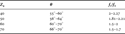
Therefore, for a chosen value of Z 4, the value of other characteristic impedances, which can be obtained by simple steps mentioned before, should be in the fabrication limit (20–120 Ω). This limitation leads to some other limitations for θ and also for frequency ratio f 2/f 1.
Table 2 shows the ranges of θ and f 2/f 1 in which other characteristic impedances have practical values for some values of Z 4.
Table 2. Practical values of θ and f 1/f 2 for a chosen Z 4.
For instance, to design a PD with dual frequencies at 1 and 2 GHz, the design procedure is as follows:
The First step (finding the electrical length of each arm): according to the first and second frequency band we get, f 2/f 1 = 2 so from equation (16), θ = 60°.
Second step (finding Z 4 and Z 2): from Table 2 the best choice for the value of Z 4 is 50 Ω also from equation (14), Z 2 = 50 Ω.
Third step (finding Z p and Z 3): from equation (9), Z p = 37.5 Ω and from equation (15), Z 3 = 32.57 Ω.
The last step (finding Z 1 and Z v): by solving the two equations of (4) and (6), the two parameter of Z 1 and Z v are derived as 33.62Ω and 37.3108Ω, respectively.
III. SIMULATION AND EXPERIMENTAL RESULTS
As an experimental verification, a four way dual-band GPD, which is designed to operate at dual frequencies of 1 and 2 GHz, is fabricated using microstrip TL. The type of substrate of the microstrip line is RO4003C with a thickness of 0.508 mm, relative permittivity of 3.55 and loss tangent of 0.0027.
The design parameters for f 2/f 1 = 2, Z ° = R = 50 Ω and for chosen Z 4 = 50.78 Ω, are as follows:
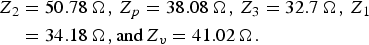 $$\eqalign{ Z_2 &= 50.78\,{\rm \Omega}, \,Z_p = 38.08\,{\rm \Omega}, \,Z_3 = 32.7\,{\rm \Omega}, \,Z_1 \cr &= 34.18\,{\rm \Omega}, {\rm and}\,Z_v = 41.02\,{\rm \Omega} {\rm.}} $$
In order to have a planar structure that its implementation is less complicated than other N way dividers, a back-to-back configuration method is applied to design the proposed four-way dual-band PD.
Figure 4 shows the picture of the fabricated four-way dual-band GPD. There are two layers to implement this PD. Ports 1–5 are placed on the top layer, while the isolation resistors are implemented on the bottom layer.

Fig. 4. Fabricated four-way dual-band GPD: (a) top layer, (b) bottom layer.
In addition, Fig. 5 shows the simulated and measured scattering parameters of the proposed GPD. At the dual-frequency design of 1 and 2 GHz, the measured insertion losses from port 1 to transmission ports (port 2, port 3, port 4, and port 5) are all <1.77 dB. Also the measured return loss at all ports are more than 10 dB, and the isolation between transmission ports is higher than 20 dB.

Fig. 5. S-parameters of the proposed four-way dual-band GPD.
Figure 6 shows the phase and amplitude imbalance at output ports. It can be seen that the maximum measured differential phase between the four output ports is 6°, and the maximum measured amplitude imbalance between the power level at four transmission ports is around 1 dB at the dual frequency 1 and 2 GHz.
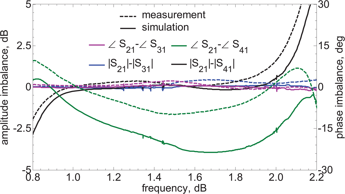
Fig. 6. Phase and amplitude imbalance of the proposed GPD.
IV. CONCLUSION
In this paper, a simple four-way structure of Gysel-type PD has been proposed for high-power applications, which provides a dual-band operation. For this purpose, an open- and a short-circuit stubs have been used. In order to overcome the difficulties of fabrication a back-to-back configuration method has also been applied. As an example, a four-way GPD operating at two frequencies, has been designed, fabricated, and measured. There has been a good agreement between both simulation and measurement results of this high PD.
 Elham Moradi was born in Kerman, Iran, in 1988. She received B.Sc. and M.S. degrees in Electrical Engineering from Shahid Bahonar University of Kerman, Kerman, Iran, in 2010 and 2015, respectively. Her current research interests include microwave power-dividing technology and passive microwave devices, circuits, and systems.
 Ali-Reza Moznebi received the B.S. degree from O.T.F. University, Fars, Iran, in 2013, and the M.S. degree from Shahid Bahonar University of Kerman, Kerman, Iran, in 2016, both in Electrical Engineering. He is currently working toward the Ph.D. degree in Electrical Engineering at Shahid Bahonar University of Kerman. His research interests include microwave/millimeter-wave power-dividing technology and microwave/millimeter-wave devices, circuits, and systems. He is also the recipient of the Outstanding Student Award in the Faculty of Engineering in 2016.
 Kambiz Afrooz was born in Baft, Iran, in 1983. He received the B.Sc. degree from Shahid Bahonar University of Kerman, Kerman, Iran, in 2005, M.Sc. and Ph.D. degrees from Amirkabir University of Technology (Tehran Polytechnic), Tehran, Iran, in 2007 and 2012, all in Electrical Engineering. In May 2011, he joined the CIMITEC Group, University Autonoma de Barcelona (UAB), Barcelona, Spain, as a Visiting Student. He is currently an Associate Professor with the Electrical Engineering Department, Shahid Bahonar University of Kerman, Kerman, Iran. His research interests are in the areas of computer-aided design of active and passive microwave devices and circuits, computational electromagnetic, modeling and simulation of high-speed interconnects, metamaterial transmission lines, and substrate-integrated waveguide structures. He is also the recipient of the Electrical Engineering Department Outstanding Student Award in 2007.
 Masoud Movahhedi was born in Yazd, Iran, in 1976. He received the B.Sc. degree from Sharif University of Technology, Tehran, Iran, in 1998, and the M.Sc. and Ph.D. degrees from Amirkabir University of Technology, Tehran, in 2000 and 2006, respectively, all in Electrical Engineering. In 2005, he was with the Institute for Microelectronics, Technische Universitt Wien, Vienna, Austria, as a Visiting Student. He is currently an Associate Professor with Electrical and Computer Engineering Department, Yazd University, Yazd. His current research interests include the computer-aided design of microwave integrated circuits, computational electromagnetic, semiconductor high-frequency RF modeling, and metamaterials. Dr. Movahhedi was a recipient of the GAAS-05 Fellowship sponsored by the GAAS Association to young graduate researchers for his paper presented at GAAS2005. He was also a recipient of the Electrical Engineering Department Outstanding Student Award in 2006.