I. INTRODUCTION
Radio frequency micro-electro-mechanical-systems (RF MEMS) research has experienced a paradigm shift from the early days of its introduction back to 1990s, as may be recognized from the current efforts focused on multidimensional product-grade topologies rather than device prototypes aiming only for good RF performance. One may appreciate such a research trend by noting that RF MEMS technology has already demonstrated its potential as an enabling platform offering favorable RF and millimeter-wave properties through several excellent papers in the literature [Reference Rebeiz1, Reference Lucyszyn2]; but it is not until some of its critical bottlenecks are solved, including dielectric charging in capacitive switches [Reference van Spengen3], contact degradation in ohmic switches [Reference Toler, Coutu and McBride4], mechanical fatigue and creep [Reference Huang, Vasan, Doraiswami, Osterman and Pecht5], environmental robustness [Reference Goldsmith, Hwang, Gudeman, Auciello, Ebel and Newman6], and packaging [Reference Tilmans7], may this technology really thrive against the competing semiconductor alternatives.
The fabrication process plays a major role in setting the extent of the mentioned bottlenecks of the RF MEMS technology. Examples include, utilization of alternative dielectrics to mitigate dielectric charging in capacitive devices [Reference Goldsmith8], prudent choice of hard contact materials to prolong the lifetime of ohmic contact devices [Reference Chen9], careful selection of the structural metal to reduce temperature sensitivity [Reference Palego10] or mechanical failure [Reference Hsu, Koslowski and Peroulis11], and the development of effective packaging strategies to reduce the adverse effects of humidity and contamination [Reference Forehand and Goldsmith12, Reference Maciel, Majumder, Lampen and Guthy13]. The importance of the adopted fabrication process can be also highlighted from a yet different perspective, as it might also introduce some uniformity and repeatability problems on its own. For instance, the sacrificial layer employed in the surface micromachining-based approaches might cause step-ups in the structural layer due to the underlying topology (unless planarization is used), which might in turn cause stiffness variations (translating to pull-in voltage deviations) and typically nonuniform post-release deflection of the mechanical member (along with a variable air gap). Another example is the difficulty in setting a repeatable and predetermined stress level within the structural layer, which is complicated by the combined contributions of the sacrificial layer, the structural layer, and anchor reinforcement members [Reference Topalli, Civi, Demir, Koc and Akin14–Reference Cetintepe16].
This work proposes an alternative fabrication process to alleviate some of the previously described bottlenecks of the RF MEMS technology and exercise more control on the process-related issues. The proposed fabrication process uses two separate wafers to optimize the properties of the structural layer and the underlying layers individually in a convenient manner. The structural layer consists of a stack of layers deposited on one of the blank wafers, which permits one to realize flat MEMS members and maintain more control over their residual stress as well as the thermal sensitivity of the overall stack. The process does not employ a sacrificial layer; instead, a recess formed on the other wafer provides the air gap between the MEMS member and the underpass signal line. Patterned MEMS members are transferred to the base wafer by bonding these wafers together using the Au-Au thermocompression bonding technique [Reference Min and Rebeiz17]. Although the proposed work bears some similarities to [Reference Milanovic, Maharbiz and Pister18] from these described perspectives; wafer-level bonding feature, increased process throughput and capacitive switching nature of the former mainly differentiates it from the die-level flip-chip approach and ohmic switch configuration of the latter.
The following sections are organized as follows. Section II describes the flow of the proposed fabrication process, and focuses on the details of each step over a sample capacitive RF MEMS switch layout, which had been previously adopted as a test vehicle in the previous process evaluations [Reference Cetintepe16]. Section III, next, elaborates on the measurement results of these fabricated switch samples. In particular, Section III-A presents the optical profile measurements of the fabricated MEMS bridges, and highlights key aspects of these profiles for further correlation with other measurements. Section III-B discloses the measured millimeter-wave performance of the fabricated RF MEMS switches at up and down-states, and compares these data with the expectations from full-wave simulations. Section III-C then delves into the electromechanical properties of the fabricated switches, and supports the gathered experimental data through coupled-field electromechanical simulations. Afterwards, Section III-D examines the temperature sensitivity of the fabricated MEMS bridges through thermal stress tests. Finally, the paper ends with the conclusions drawn from this study.
II. FABRICATION PROCESS FLOW
Figure 1 illustrates the flow of the proposed fabrication process. The process starts with two separate wafers: a structural silicon wafer and a base glass wafer (Step 1 in Fig. 1). The stack layers of 0.1 µm SiO2/0.2 µm SixNy/1 µm Cr–Au are deposited and patterned on the silicon handle wafer (Steps 2A–3A in Fig. 1) with an overall tensile stress less than 50 MPa to form the MEMS bridges. Next, 1.5-µm-deep recesses are etched on the glass substrate using a buffered hydrofluoric acid (BHF) solution, to define the air gap for the capacitive RF MEMS switches (Step 1B in Fig. 1). During this recess etching step, a 0.3-µm-thick amorphous-Si acts as the masking layer. Then, a 1-µm-thick Cr–Au is sputtered and patterned on the glass wafer to form the coplanar waveguide (CPW) metallization (Step 2B in Fig. 1). After that, a 0.3-µm-thick PECVD SixNy dielectric is deposited onto the base metallization and patterned for DC isolation purposes (Step 3B in Fig. 1).

Fig. 1. Proposed fabrication process flow.
Figure 2(a) shows an optical micrograph of the base metallization and dielectric layers on the base wafer prior to the bonding step. Figure 2(b) provides a close-up scanning electron microscopy (SEM) view for the glass recess region that defines the air gap between the base metal underpass and the MEMS bridge.
Fig. 2. (a) Base metal and dielectric layers of an RF MEMS switch patterned on the base wafer, viewed prior to the bonding step. (b) An SEM view of the glass recess region.
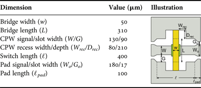
Following the patterning of the structural and base wafers, these wafers are subsequently aligned with each other and bonded using the Au–Au thermocompression bonding technique (Step 4 in Fig. 1). Figure 3 shows the micrograph of an RF MEMS switch after this bonding step, viewed from the glass side. Next, the silicon part of the bonded wafer is thinned from 500 to 100 µm in the deep reactive ion etching (DRIE) system. Process is completed with the complete removal of the silicon handle wafer using a tetramethylammonium hydroxide (TMAH) solution (Step 5 in Fig. 1). Figures 4(a)–(c) present an optical micrograph, an SEM image, and a three-dimensional (3D) optical profilometer measurement of a released RF MEMS switch sample, respectively. Table 1 summarizes the dimensions of the fabricated switch for reference purposes [Reference Cetintepe16].
Fig. 3. Optical micrograph of an RF MEMS switch after the bonding step (prior to release), viewed through the glass wafer.
Fig. 4. An RF MEMS capacitive shunt switch fabricated with the proposed process flow: (a) microscope snapshot, (b) close-up SEM view of the MEMS bridge, and (c) 3D optical profilometer measurement.
Table 1. Switch layout dimensions.
III. MEASUREMENTS OF THE FABRICATED SWITCHES
A) Surface profile measurements
Prior to millimeter-wave and electromechanical measurements, fabricated RF MEMS switch samples are inspected using an optical profilometer first in order to confirm the vertical design dimensions. Figure 5 shows the two-dimensional (2D) profile of a typical MEMS bridge sample. One notices from Fig. 5 that the 1.55-µm-deep recess in the glass wafer agrees with the designed value of 1.50 µm. Another immediate observation is that the MEMS bridge exhibits curling along its width dimension, with an approximate radius of curvature of ρ = 450 µm. This lateral bending behavior is attributed to the strain mismatch between the individual layers of the MEMS bridge stack as described in [Reference Huang and Zhang19, Reference Liu20]. This side effect was not considered during the design of these first-generation devices; but rather the layer stack arrangement and individual stress levels were optimized from an axial stiffness (hence, pull-in voltage) perspective only.
Fig. 5. Measured 2D profile of a sample RF MEMS switch showing the gradient-induced bending along its width. The inset depicts the location of the cut along the MEMS bridge.
Mentioned stress gradient-induced bending, together with the reduced air gap caused by the bonding step (1.15 µm versus the design value of 1.20 µm), not only increases the up-state capacitance of the RF MEMS switches slightly beyond their nominal value; but it also alters their electromechanical characteristics at the down-state as will be explained in the following subsections.
B) Millimeter-wave measurements
Millimeter-wave characteristics of the fabricated RF MEMS switch samples are investigated under open-environment conditions using Cascade Microtech Summit 9000 Manual Probe Station and Agilent E8361A PNA. Prior to the measurements, reference planes are set at the CPW probe tips via an off-wafer SOLT calibration performed in 10–40 GHz frequency band. For down-state measurements, the switches are actuated with a 200 Hz, 50% duty cycle, bipolar, square waveform which is applied from a custom bias waveform generator through bias-tees.
Figure 6 presents the measured S-parameters of typical switch samples at their up-state. These samples exhibit return and insertion losses which are better than 13.7 and 0.38 dB (on the average), respectively, up to 35 GHz. While these metrics remain acceptable for most applications, they clearly deviate from the nominal full-wave simulation results of ≥24.0 and ≤0.19 dB, respectively in the same frequency range. As pointed out in the previous subsection, this degradation in the up-state performance stems from the increased capacitive loading due to the curled bridge shape and slightly thinner air gap. In fact, full-wave simulation results overlaid on Fig. 6 verify this reasoning: the nominal return and insertion loss curves (dashed with diamonds) become good approximations to the measured ones (dashed with stars) when an equivalent air gap of 0.85 µm is employed in the simulations.
Fig. 6. Measured return and insertion losses of the RF MEMS switches at up-state.
Despite the slightly underachieved up-state performance compared to the design specifications, the fabricated switches still feature their low-loss property: after subtracting the reflection loss component from the insertion loss (via |S 21|2/(1 − |S 11|2)), the switches appear to present an average loss of only 0.19 dB at 35 GHz.
Figure 7 shows the measured down-state S-parameters of a typical RF MEMS switch sample, with the bias voltage taken as a parameter. One notes from Fig. 7 that the switch responds to the applied bias by gradually improving its isolation, a behavior which is indicative of a capacitive-contact improvement mechanism. The isolation level, however, stays relatively low even at high bias voltages: at 35 GHz for instance, the isolation improves only marginally from 0.97 to 2.96 dB by increasing the bias voltage from 20 to 90 V. This poor isolation response does not agree with the ones obtained from previous implementations of the same switch design [Reference Cetintepe16]. Figure 7 emphasizes this observation by overlaying (to the right vertical axis) the full-wave simulated S-parameters of the switch under normal contact conditions: for the assumed nominal contact, the switch potentially offers up to 40 dB of isolation over a tuned frequency band around 35 GHz.
Fig. 7. Measured return and insertion losses of the RF MEMS switches at down-state with bias voltage as a parameter.
In the light of the observations above, one suspects that the fabricated samples do not exhibit the predicted contact characteristics at their down-states. The following subsection explores this phenomenon in detail, and sheds some light onto the mentioned degradation in the down-state performance.
C) Electromechanical analyses
Degraded down-state performance of the fabricated RF MEMS switches warrants an additional investigation in electromechanical domain to understand the source of the problem and eliminate it in subsequent fabrication runs. Toward that goal, C–V characteristics of the previous switch sample are extracted by fitting CLR circuit models to the S-parameter dataset of Fig. 7. Figure 8 plots this experimental C–V curve along with the simulated one obtained from a coupled-field electromechanical analysis performed in ANSYS Mechanical APDL v13 [21]. The experimental C–V data in Fig. 8 agree well with the electromechanical simulation results, an observation establishing confidence on the latter to study the contact characteristics at down-state.
Fig. 8. Measured and simulated C–V curve of a sample switch.
A detailed examination of Fig. 8 reveals that the multilayer MEMS bridge incurs two distinct pull-in instabilities instead of just one: the first pull-in occurs at about 18 V, in accordance with measurements, after which the capacitance increases slowly with voltage. In this plateau region, the down-state capacitance stays at a low fraction of the available one (21–29% for this design including roughness effects), which in turn causes a low RF isolation. The capacitance does not settle to its designed value until the second pull-in occurs at about 93 V.
The contact mechanism yielding the mentioned double pull-in behavior and the associated capacitance degradation can be best understood from an inspection of the MEMS bridge deflection profile at distinct points along the C–V curve. Figure 9 depicts such simulated profiles at 0, 18, and 93 V, corresponding to the up-state, first pull-in and second pull-in states, respectively. Figure 9(a) reproduces, to a good approximation, the curled bridge profile originally shown in Fig. 5. This curled profile prevents the bridge from establishing a flat capacitive contact after the first pull-in, as shown in Fig. 9(b). At this state, the bridge stays pinned along its edges over the dielectric, offering little down-state capacitance as well as zipping due to the air layer sandwiched between the dielectric and the bridge. The pin-supported bridge gets pulled-in at 93 V a second time as shown in Fig. 9(c), a state which eliminates the previously sandwiched air layer and yields a proper capacitive-contact.
Fig. 9. Simulated deflection characteristics of the RF MEMS switch having a curled width profile: (a) at up-state, (b) after first pull-in at 18 V, and (c) after second pull-in at 93 V.
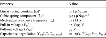
Table 2 lists the key mechanical features of the RF MEMS switch described in this subsection, along with its simulated stiffness and harmonic characteristics.
Table 2. Simulated mechanical characteristics of the RF MEMS switch.
*Force-deflection characteristics is modeled with F = k lu z + k cu z3.
†Only one pull-out state is observed due to convergence issues.
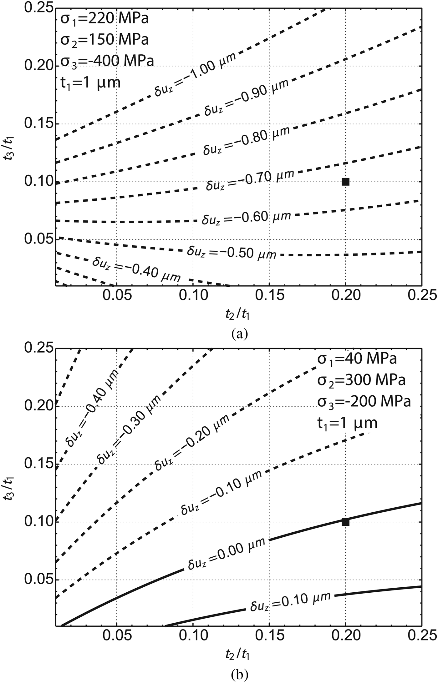
In the light of the measurements and simulation results presented so far, one realizes that the curled profile of the multilayer MEMS bridge is mainly responsible for the performance degradation of the fabricated RF MEMS switches. Elimination of this lateral bending, therefore, will help eliminate most of the shortcomings of this alternative RF MEMS fabrication process. One potential remedy to mitigate this lateral bending is to choose a proper residual stress and/or thickness combination for the individual layers in the structural stack. To illustrate the procedure, we consider two stacks with different residual stress states, and calculate the lateral deflection as a function of relative layer thicknesses assuming free–free end conditions [Reference Huang and Zhang19, Reference Liu20]. These free–free end conditions approximately model the MEMS bridge along its width dimension (excluding the Poisson effect of axial confinement at the anchors) and permits one to calculate the maximum lateral bending through
 $$\delta u_z=w^2 /8\rho ,$$
where w is the bridge width and ρ is the radius of curvature. Figure 10 shows the results of two sample simulations. In particular, Fig. 10(a) corresponds to the originally modeled stack and it shows that the lateral deflection is negative with respect to the bridge center (the bridge curls up) for practical ranges of layer thicknesses. The black square at (0.2, 0.1) marks the realized stack and its lateral deflection reads 0.67 µm, which is indeed close to the measured 0.7 µm value. Plotted contours for this particular stress state suggest thinner SixNy and SiO2 layers as one way to reduce the lateral bending. For a modified stress state, however, these contours might suggest alternative means to reduce lateral bending as Fig. 10(b) demonstrates: through prudent choice of the layer stresses, one might achieve a perfectly flat bridge for some thickness combinations, the (0.2, 0.1) combination now being one of them.
Fig. 10. Simulated lateral deflection of the MEMS bridge for different stack configurations: (a) original stress state and (b) modified stress state.
D) Thermal stress tests
In addition to millimeter-wave and electromechanical tests described in the earlier subsections, temperature sensitivity of the fabricated switches is also investigated via thermal stress tests. For this purpose, the switch samples are maintained at 250°C for 1 h over a hotplate, the conditions of which emulate the thermal load needed for a packaging process currently under development. Figure 11 compares the measured optical profile of a thermally stressed switch sample to its original state. The out-of-plane deflection due to the thermal load appears to be negligible in Fig. 11 (about 30 nm difference over the overlap area), an observation suggesting minimal RF and electromechanical performance modification for the fabricated switches after exposure to a considerable thermal load. Demonstrated temperature insensitivity of the multilayer stack translates to a thermally robust RF MEMS switch, which can potentially remain stable after packaging.
Fig. 11. A comparison between the measured surface profiles of a switch sample in its pristine and thermally stressed states. The inset shows the cut location along the MEMS bridge.
IV. CONCLUSION
In this paper, a process flow is described for the fabrication of RF MEMS capacitive switches with a stacked structural layer. Two wafers are processed separately in the fabrication flow: the base wafer includes the transmission lines and the DC isolation dielectric, whereas the structural wafer has a stack of SiO2/SixNy/Cr–Au layers deposited and patterned in order to form the MEMS bridges. These two wafers are then bonded using Au–Au thermocompression bonding, and the RF MEMS switches are subsequently released by thinning and complete etching of the silicon handle wafer by DRIE and TMAH solution, respectively.
The proposed process offers a number of advantages compared with the conventional surface micromachining-based ones. First, the proposed process flow does not include a sacrificial layer – the capacitive gap is formed by etching a recess region in the base wafer, whose depth can be adjusted to arbitrary values in a controlled manner. In addition, the flatness of the bridge is not affected due to the underlying topology, because the bridge is patterned over a blank wafer prior to bonding. Moreover, the structural layer can be engineered out of several layers with desired mechanical and thermal properties by controlling the material types, layer stresses, and the thicknesses. Furthermore, the suspended bridges are robust against large thermal loads such as 250°C (as typically required for packaging) since the bonding process is performed at a higher temperature of 400°C, and the bridge consists of stacked layers compensating the effects of thermal loads. Finally, the fabrication process requires fewer masks and process steps, owing to the elimination of electroplating (for anchor reinforcement) and planarization steps.
The fabrication process disclosed in this work constitutes its first generation as a means to realize RF MEMS switches. These first-generation RF MEMS switch samples are characterized in millimeter-wave and electromechanical domains mostly for design verification purposes. In particular, millimeter-wave measurements demonstrate up-state return and insertion losses better than 13.7 and 0.38 dB, respectively, over 10–35 GHz band; while the switches present limited down-state isolation even at high-bias voltage levels (about 3 dB at 35 GHz, at 90 V). These measured electrical metrics are noted to fall short of the full-wave simulation results and those measured from earlier implementations of the same switch design. Optical profile measurements and electromechanical simulations help identify the reason for this discrepancy as the lateral bending of the multilayer MEMS bridge: The strain mismatch between individual layers of the MEMS bridge induces a lateral bending profile along its width, which not only increases the up-state capacitance and degrades the up-state RF performance; but also alters the contact mechanics in down-state to result in a C–V curve having two pull-in instabilities and a significantly reduced down-state capacitance (hence RF isolation). It follows from these observations that later-generation RF MEMS switches can be fabricated with a significantly improved RF and electromechanical performance by a careful mechanical design of the structural layer stack.
ACKNOWLEDGEMENTS
The authors would like to thank Orhan Akar, Ilker Comart, Mert Torunbalci, Akin Aydemir, and the METU-MEMS Center staff at Middle East Technical University for their help and support on device fabrication. This work is partially supported by TUBITAK (Project Number: 109A008) and the METU-MEMS Project, which is funded by the EU FP7 Program FP7-REGPOT-2009-1 under Grant Agreement Number 245856.
Cagri Cetintepe received his B.Sc. and M.Sc. degrees in Electrical and Electronics Engineering, with high honors, from Middle East Technical University (METU), Ankara, Turkey, in 2007 and 2010, respectively. From 2007 to 2009, he worked as a Research Assistant in METU-MEMS Application and Research Center, and focused on RF MEMS research. Since 2010, he has been a Teaching and Research Assistant at the Electrical and Electronics Engineering Department, METU, where he is currently pursuing his Ph.D. studies. His scientific interests include RF MEMS switches and phase shifters, surface micromachined lumped components, microwave and millimeter-wave instrumentation, and radar applications.
Ebru Sagiroglu Topalli received her B.S., M.S., and Ph.D. degrees with high honors in Engineering Physics from Ankara University, Ankara, Turkey, in 1999, 2001, and 2008, respectively. Between 1999 and 2004, she worked as a Research Engineer at Ankara University at the Department of Engineering Physics. She received her graduate fellowship provided by the Scientific and Technical Research Council of Turkey (TUBITAK) between 2000 and 2004. She worked as a Senior Process Engineer in MEMS Research and Application Center at Middle East Technical University (METU) between 2004 and 2010. She was giving guidance/assistance to various projects related with MEMS inertial sensors, BioMEMS, and RF MEMS particularly for lithography, wafer bonding, metal deposition, and etching steps in this center. Since 2012, Dr. Topalli has been employed as a senior project researcher in the RF MEMS Group at METU. Her major research interests include development of microfabrication and packaging technologies for MEMS sensors.
Simsek Demir received his B.Sc., M.Sc., and Ph.D. degrees in Electrical and Electronics Engineering from Middle East Technical University (METU), Ankara, Turkey, in 1991, 1993, and 1998, respectively. From 1991 to 1998, he was a research assistant in METU. In 1998–1999, he contributed to the atmospheric radar antenna design in IRCTR, TU-Delft, Netherlands. Since 2000, he is a Professor in the Electrical and Electronics Engineering Department, METU. His scientific interests include microwave and millimeter-wave active and passive component and system design, analysis, and modeling. Exploitation of RF MEMS technology toward industrial use, power amplifier design, modeling and implementation, and radar applications are some of his particular research topics. Dr. Demir is a recipient of several awards, including NATO A2 fellowship which supported him as a visiting researcher in the University of Massachusetts at Amherst, in 1995.
Ozlem Aydin Civi received her B.Sc., M.Sc., and Ph.D. degrees in 1990, 1992, and 1996, respectively, in Electrical and Electronics Engineering Department of the Middle East Technical University (METU) in Ankara, Turkey. She was a Research Assistant in METU between 1990 and 1996. In 1997–1998, she was a Visiting Scientist at the ElectroScience Laboratory, Ohio State University. Since 1998, she has been with the Department of Electrical and Electronics Engineering, Middle East Technical University, where she is currently a Professor. Her research interests include analytical, numerical, and hybrid techniques in EMT problems especially fast asymptotic/hybrid techniques for the analysis of large finite periodic structures, multi-function antenna design, reconfigurable antennas, phased arrays, reflect arrays, and RF MEMS applications. Dr. Civi has published more than 130 journal and international conference papers. She is an Associate Editor of the IEEE Transactions on Antennas and Propagation.
Tayfun Akin received his B.S. degree in Electrical Engineering (with high honors) from Middle East Technical University (METU), Ankara, in 1987, and the M.S. and Ph.D. degrees in Electrical Engineering from the University of Michigan, Ann Arbor, in 1989 and 1994, respectively. Since 1995, 1998, and 2004, he has been an Assistant Professor, Associate Professor, and Professor, respectively, with the Department of Electrical and Electronics Engineering, METU, Ankara, Turkey. He is the Director of METU-MEMS Center, which has a 1300 m2 cleanroom area for 4”–8” MEMS processing. He raised and managed over 65 M USD funding for several national and international projects, including EU FP6, FP7, NATO SfS, and NSF-USA projects. His research interests include MEMS, microsystems technologies, uncooled infrared detectors and readout circuits, inertial microsensors, silicon-based integrated sensors and transducers, and analog and digital integrated circuit design. Dr. Akin has authored/co-authored over 150 international journal and conference papers.