


Introduction
The proliferating growth of next-generation network demands high data rate, low latency, and feasible cost [Reference Ranaweera, Wong, Nirmalathas, Jayasundara and Lim1]. These requirements have caused pronounced challenges to the existing wireless and optical networks. These overheads can be met by the radio over fiber (RoF) technology that provides an appropriate infrastructure for building centralized/cloud radio access network (C-RAN).
During this era, C-RAN was proposed [2] to autonomies the baseband processing units and amalgamate them into a centralized baseband unit (BBU) pool, which simplifies each base station to a remote radio head (RRH), possibly relying on non-conventional beamforming strategies, which exploit the time [Reference Masotti, Francia, Costanzo and Rizzoli3, Reference Aslam, Xia and Hadi4] as well as the frequency [Reference Wang, So and Farina5, Reference Khurshid, Khan, Siddiqui, Rashid and Hadi6] as an additional degree of freedom. In addition, C-RAN also enables the radio coordination among multiple cells [Reference Wang, Yu, Ying, Zhang, Lu, Xu, Cheng, Ma and Chang7–Reference Hadi10]. This divides the architecture into two main segments, i.e. backhaul (comprising from mobile network to BBUs) and fronthaul (BBUs to RRHs) (see Fig. 1).

Fig. 1. C-RAN schematic presenting optical fronthaul.
In order to accommodate broadband wireless services from various radio access technologies (RATs), both analog and digital fronthaul architectures have been investigated. Analog-radio over fiber (A-RoF) technologies, the essential block diagram of which can be appreciated in Fig. 2, considering the green (A-RoF) branches, feature low-cost, spectral efficiency, simplicity of realization, and can be applied both in outdoor and in-building scenarios, exploiting different kinds of optical fibers [Reference Visani, Okonkwo, Shi, Yang, van den Boom, Tartarini, Tangdiongga and Ton Koonen11–Reference Meslener16]. However, the A-RoF solution suffers from non-linearities introduced by both microwave and optical parts [Reference Kurniawan, Nirmalathas, Lim, Novak and Waterhouse17–Reference Roselli, Borgioni, Zepparelli, Ambrosi, Comez, Faccin and Casini25]. In order to subdue these non-linearities, many methods have been proposed among which analog and digital techniques are widely used. In particular, an analog predistortion method was addressed in [Reference Fuochi, Hadi, Nanni, Traverso and Tartarini26] that compensates the laser non-linearities. Digital pre-distortion (DPD), which is followed by a digital-to-analog conversion to maintain the A-RoF scheme, based on behavioral modeling of laser was proposed in [27]. Similarly, DPD linearization techniques which use memory and generalized memory polynomials have been applied to non-linear RoF links based on different optical transmitters, including those based on VCSELs [Reference Vieira and Gomes28–Reference Hadi, Jung, Ghaffar, Traverso and Tartarini30].
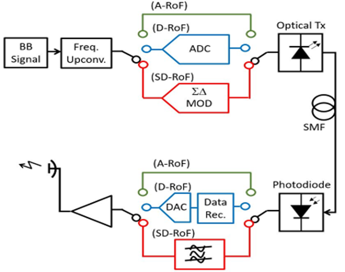
Fig. 2. Block schematic of A-RoF, D-RoF, and ΣΔ-RoF downlinks. BB, base band; Freq. Upconv., frequency upconverter; ADC, analog-to-digital converter; ΣΔ MOD, sigma-delta modulator; Tx, transmitter; SMF, single mode fiber; Data Rec., data recovery block; DAC, digital-to-analog converter. Note that the SD-RoF scheme can also be implemented swapping the positions of the ΣΔ MOD block and of the frequency upconversion block. This last configuration of the ΣΔ-RoF link is the one utilized in the present work.
All these solutions can however risk to reduce the simplicity and the cost-effectiveness of A-RoF links, which should constitute their main attractive features.
On the other hand, digital mobile fronthauls (D-MFHs) based on the digital-radio over fiber (D-RoF) technique are not affected by the non-linear effects typical of A-RoF systems [Reference Lim, (Thas) Nirmalathas, Lee, Novak and Waterhouse31–33]. In Fig. 2, considering the blue (D-RoF) branches, a typical D-RoF architecture can be visualized.
The common public radio interface (CPRI) that was proposed by the CPRI cooperation, Nokia, Bell Labs, Ericsson, Huawei, Orange, and NEC was adopted as the D-MFH interface [Reference Hadi34]. However, when CPRI was employed as a digitization interface developed for narrowband RATs, due to its limited spectral efficiency, it had limited scalability. Moreover, it also requires a very high data traffic in the fronthaul network segment, implying the use of expensive high-performance analog-to-digital and digital-to-analog converters [Reference Pessoa, Tavares, Coelho and Salgado35]. Therefore, an alternative possibility, which can overcome these bottlenecks, would be worthwhile.
This solution can be pursued by employing sigma-delta (ΣΔ) modulation, realizing in this way a technique, which can be defined as sigma-delta radio over fiber (ΣΔ-RoF), combining the advantages of both methods, i.e. A-RoF and D-RoF.
An example of realization of a ΣΔ-RoF system can be already appreciated in Fig. 2, considering the red (ΣΔ-RoF) branches. It can be seen that in the ΣΔ-RoF systems, the signal, before being converted to the optical domain by the optical transmitter, undergoes the ΣΔ modulation. This operation, exploiting a high-speed digital oversampling of the modulating signal with 1-bit resolution, allows to reach a high immunity to non-linearities. At the same time, it realizes the so-called noise shaping, which places most of the noise power out of the useful signal bandwidth [Reference Breyne, Torfs, Yin, Demeester and Bauwelinck36–Reference Hadi, Traverso, Tartarini and Jung38].
As shown in Fig. 2, at the receiver end, after the optical-to-electrical conversion, performed by a photodetector, a band-pass filter (BPF) guarantees the correct digital-to-analog conversion of the signal as well as the spectral emission requirements, by filtering the out-of-band quantization noise.
It can then be observed that the ΣΔ-RoF technique proves particularly convenient in the realization of the fronthaul downlink, where the transmitting section is located at the BBU, while the receiving section is at the RRH. Indeed, the cost of the ΣΔ modulator can in this way be shared by many users, while the RRH structure is maintained simple, without the installation of active devices. Following the same idea, solutions for the fronthaul uplink which can maintain the RRH simple configuration should be pursued, not excluding the A-RoF one [Reference Breyne, Torfs, Yin, Demeester and Bauwelinck36]. In [Reference Hadi, Aslam and Jung39], the authors assessed the performances of a ΣΔ-RoF system with the ΣΔ modulated signals were coming from a MATLAB code, and were then loaded to a pulse pattern generator (PPG).
As an evolution of such work, in this paper, we report a realistic, suitably modified ΣΔ-RoF system, by means of a laboratory implementation on a commercial FPGA. The attractive features of ΣΔ-RoF will be confirmed, and some aspects to be appropriately taken into account to optimize the final system performance will be put into evidence. The paper is organized as follows. Section 2 briefly discusses the system description and experimental setup. In Section 3, the performance analysis of the ΣΔ RoF system is presented in terms of adjacent channel leakage ratio (ACLR) and error vector magnitude (EVM), allowing to identify optimized values for some operating quantities. Finally, conclusions are drawn in Section 4.
The novelty of the work is reported as follows:
• Although D-RoF are good alternative to A-RoF, the fact that the remote site requires the employment of a high bandwidth DAC is a considerable disadvantage, we propose a solution for the implementation of future RoF systems based on the usage of a band-pass sigma-delta (SD) modulator at the transmitter side, working as a 1-bit ADC.
• In the fronthaul scenario under observation, it was required that an efficient real-time transmission is made. For this, we implemented the method on FPGA. The transmission distance covered was 10 km while 20 MHz LTE frame was used at 256 quadrature amplitude modulation (QAM) order.
• Although ΣΔ modulation has been exploited in [Reference Checko, Christiansen, Yan, Scolari, Kardaras, Berger and Dittmann8, Reference Wang, Liu, Zhang, Zhu, Xu, Lu, Cheng and Chang23, Reference Hadi, Kantana, Traverso, Tartarini, Venard, Baudoin and Polleux24, Reference Breyne, Torfs, Yin, Demeester and Bauwelinck36, Reference Sezgin, Gustavsson, Lengyel, Eriksson, He and Fager37], however, as mentioned above, this work is a continuation of our work proposed in [Reference Lim, (Thas) Nirmalathas, Lee, Novak and Waterhouse31, Reference Hadi, Aslam and Jung39] where we would like to stress upon the advantages ΣΔ RoF can bring as compared to A-RoF and D-RoF.
• The comparison study is evaluated where all three types of RoF systems are compared.
Sigma-delta RoF system realization
Figure 3(a) shows the structure of a ΣΔ-modulator. It is obtained by replacing the quantizer, the 1-bit ADC, in the first-order ΣΔ-modulator with a copy of a first-order ΣΔ-modulator. Considering again ideal components, the output, y(kT), takes the form:

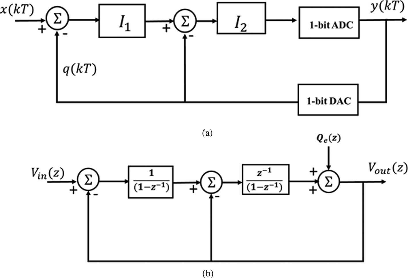
Fig. 3. Block diagram representing the second-order ΣΔ modulation (a) structure and (b) its Z transfer domain model.
Equation (1) represents that output is a delayed quantized input signal with a second-order differencing of the quantization noise. Figure 3(b) shows its linear z-domain model, from which the NTF and the STF can be obtained:

where V out(z) and V in(z) are output and input, respectively, while Q e(z) represents the quantization noise. The integrator blocks I 1 and I 2 are expressed, respectively, by I 1 = 1/(1 − z −1) and I 2 = z −1/(1 − z −1). In (2), STF is the signal transfer function, while NTF is the noise transfer function.
The magnitude of the NTF is evaluated as follows:

Similarly, the in-band noise power of the output for the second-order SDM can be calculated as:

where S p(f) is the power spectral density (PSD) and OSR is over sampling ratio. If we consider again a sin wave as the input with amplitude A, the output becomes:

Since |STF|2 = 1.
The signal to noise ratio (SNR) is computed as follows:

The frequency response of the second-order $\sum \Delta M$ is given in Fig. 4(a) in linear scale and in dB scale in Fig. 4(b). It also shows that the quantization noise is highly attenuated in the band of signal near 0 and is eminently invigorated in high, out of band frequencies, more than it undergoes in case of first-order $\sum \Delta M$
 [Reference Wang, Liu, Zhang, Zhu, Xu, Lu, Cheng and Chang23].

Fig. 4. Frequency response of second-order $\sum \Delta M$ : (a) magnitude in linear scale, (b) magnitude in dB.
From Eq. (6), the doubling of the OSR leads to an increase of the SNR by 15 dB, which means that to achieve the same value of SNR, the second-order $\sum \Delta M$ needs a lower OSR, leading to a lower sampling frequency, when compared with the first-order $\sum \Delta M$
 . The downside is the increased total noise power, as stated previously.
The details of the ΣΔ-M model implied can be found in [Reference Fouto and Paulino40–Reference Hadi, Nanni, Venard, Baudoin, Polleux and Tartarini43].
Figure 5 shows the experimental test bed utilized for this work. Let us consider an in-phase denoted as I and quadrature represented by Q baseband signals. This pair of baseband signals is sigma-delta converted by 1-bit ΣΔ modulators at 6 GSa/s. The unwanted and relatively high quantization noise will be filtered out at the receiver. The sigma-delta modulated baseband signals are then up-converted with carrier frequency f c = 3 GHz. This is followed by the electrical-optical conversion according to the typical A-RoF approach.
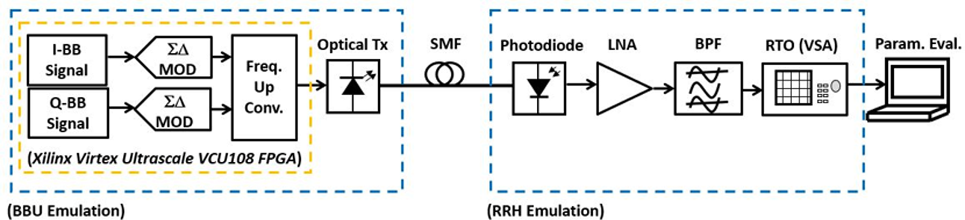
Fig. 5. Experimental test bed for real-time implementation of sigma-delta radio over fiber system. I-BB, Q-BB, in-phase and quadrature baseband, respectively; ΣΔMOD, sigma-delta modulator; Optical Tx, optical transmitter; SMF, single mode fiber; LNA, low noise amplifier; BPF, band-pass filtering; RTO, real-time oscilloscope; VSA, vector signal analyzer; Param. Eval., parameters evaluation.
The optical converted signals are transmitted over standard single mode fibers (standard SMFs). At the receiver, the photodiode converts the optical signal back to electrical domain followed by a reconstruction BPF which filters out most of the quantization noise.
The module has a capacity to implement 4x parallel transmitters, and 4 ΣΔ-RoF links of the kind of the one represented in Fig. 5 have consequently been realized to fully exploit its potentiality. To bring the optical signal to the respective RRHs, a cable composed of SMFs is utilized, terminated with MTP connectors. For simplicity, the results referred to only one lane proof will be shown.
The baseband signal generation, its sigma-delta modulation, and up-conversion represented in Fig. 5 are implemented on Xilinx Virtex Ultrascale VCU108 FPGA Evaluation Kit. After the FPGA performs sigma-delta modulation followed by up-conversion, the 1-bit modulated stream is fed to Module QSFP28-PIR4-100G (1310 nm distributed feedback (DFB) laser) employed for the electrical-optical conversion to transmit over SSMF. The module used has allowed min power = −9.4 dBm, max power = 2.0 dBm in the transmitting mode and min power = −12.66 dBm, max power = 2 dBm in the receiving mode, however, it can be pushed below the safe limits for seeing the trend. The received signals are then fed to respective RRH units having a low noise amplifier that amplifies the received signal and sends it to an analog BPF tuned at the RF signal center frequency. A properly designed BPF eliminates the out-of-band quantization noise shaped by the SDM and guarantees that the spectral mask requirements are met. The band-pass filtered signals are fed to UXR1004A Infiniium UXR real-time oscilloscope that runs the vector analysis software for post processing of data and parameters evaluation. The noise current spectral density around f c is 16 ${\rm pA/}\sqrt {{\rm Hz}}$ . The module QSFP28-PIR4-100G has four transmitters where each one has a clock data recovery to resample the data if needed. The parameters and values are given in Table 1.
Table 1. System parameters

Table 1 below shows the detail of setup and parameters utilized.
Experimental results and discussion
Firstly, the performance of the system is measured by estimating the ACLR. ACLR is defined as follows [44]:

Here B Al represents the lower and B Au are the upper frequency limits of one of the adjacent channel bands. Similarly, B Ul is the lower and B Uu are the lower and upper frequency limits of the useful channel bands. S(f) represents the measured PSD of the output signal.
One of the most important measurements is the leakage power in the adjacent channels. ACLR is considered as a critical specification for digital communication systems corresponding to signal distortion leaking in the neighbor channels. Leakage power influences the system capacity as it interferes with the transmission in adjacent channels. Therefore, it must be rigorously controlled to guarantee a stable system capacity. ACLR limits are given in standards for the whole system. As defined in 3GPP TS 34.122, ACLR should not be more than −33 dB at the offsets of ±1.6 MHz.
The adjacent channel power ratio of a wireless communication system is the integrated power in the carrier channel relative to the adjacent channel. The non-linearity distortion in the link can downgrade the transmission performance of an RoF system since the non-linearity can generate spurious cross-talks that may overlap with the transmitted RF signal and leak the power into the adjacent RF channels. Among all the non-linear spurious products, the third-order intermodulation distortion attracts more attention because it probably falls into the passband of a multicarrier system and is difficult to be filtered out. Excessive non-linearity limits the power of the input signal, therefore degrading the dynamic range performance. Usually, we use robust distortion measure called as ACPR when we study the non-linearity-induced cross-talk in an RoF system. ACPR is the wideband equivalent to the input intercept point of order 3 case.
Figure 6 represents the experimental evaluation of ACLR with respect to changing fiber length L and input RF power P IN, respectively. It can be appreciated that for a given P IN, ACLR increases with increasing L. Conversely, for a given L, higher values of P IN lead to higher ACLR values. The worst value reported in Fig. 6 is therefore the one corresponding to P IN = 0 dBm and L = 10 km, for which it is ACLR = −29.59 dBc. Figure 6 refers to the transmission of a 256 − QAM signal, with symbol equal to 400 MBd. Note however that the ACLR evaluation has been performed transmitting a 256 − QAM signal, with the symbol rate that ranged from 100 to 400 MBd, and the behavior of ACLR resulted to be substantially the same regardless of the symbol rate considered.

Fig. 6. Measured ACLR at the receiving end of the SD-RoF system, versus input power and for varying values of L.
In order to keep ACLR at lower values, which means lower detriment given to adjacent channels from the creation of undesired distortion terms, it should be then appropriate to keep P IN as low as possible, within the range allowed.
To better specify this requirement, the system performance is measured by EVM. EVM can be mathematically expressed as [Reference Hadi, Aslam and Jung39]:

where N is the total number of symbols received, I j is the received in-phase component of the j − th received symbol, while $\tilde{I}_j$ is the ideal in-phase component of the same symbol. Similarly, Q j is the quadrature component of the j − th received symbol, while $\tilde{Q}_j$
 is its ideal quadrature component. The 3GPP standard has set an EVM limit for LTE signals modulated by 256 QAM format to be 3.5% [Reference Vieira and Gomes28].
The EVM is then evaluated for varying values of P IN and for different link lengths L. For this estimation, the symbol rate was marked as 400 MBd. The obtained results are summarized in Fig. 7, where it can be seen that for a given value of L, increasing the values of the input power allows to obtain the EVM to fall below the values of 3.5%. For a given P IN, an EVM increase is observed for L going from 0.1 to 10 km, due to the increasing path loss undergone by the transmitted signal.

Fig. 7. EVM with changing input power for different lengths at 400 Mbd.
In Fig. 8, the received constellation diagram is compared when a 256 QAM signal is transmitted with 400 MBd and with P IN = 0 dBm through the minimum and maximum ΣΔ-RoF link lengths, respectively. It is observable that for L = 100 m the received constellation diagram is clean, while for L = 10 km it is rather noisier. However, looking again at Fig. 6, it can be observed that in the two cases, the EVM is respectively 1.01 and 2.48%, i.e. both configurations fall below the threshold of 3.5% set by 3GPP.

Fig. 8. Constellations corresponding to the received signal EVM with input power P IN = 0 dBm, for different lengths at 400 Mbd.
A behavior similar to the one reported in Fig. 9 is also observable for the other values of L considered. In order to summarize all the measured performances, Fig. 10 reports for each considered value of L value minimum value P IN,min, EVM<3.5% below which P IN cannot fall in order to guarantee EVM < 3.5%. It can be appreciated that when transmitting at 400 Mbd it is P IN,min, EVM<3.5% = −12 dBm for L = 0.1 km, while it is P IN,min, EVM<3.5% = −6 dBm for L = 10 km.

Fig. 9. Reports the EVM for 10 km link length with symbol rates ranging from 100 to 400 MBd, at different values of input power P IN. It is visible that performing an increase from the value P IN = −16 dBm, for which it is EVM>3.5% for all the symbol rates considered, the EVM monotonically decreases and, starting with the 100 MBd and ending with the 400 MBd case, the transmission is gradually attainable while respecting the EVM limit.

Fig. 10. Minimum RF input required to achieve a determined baud rate for different link lengths.
In line with the considerations developed above, the values of P IN,min, EVM<3.5% can be identified as the optimized ones, since they maintain the ACLR at the lowest possible value, while allowing the received EVM to accomplish the 3GPP requirement. As far as the range of the power of the optical transceiver QSFP28-PIR4-100G is concerned, the minimum power allowed is −12.66 to 2 dBm (receiving mode) and −9.4 to 2 dBm (transmitting mode)[Reference Hadi, Nanni, Polleux, Traverso and Tartarini45]. In our experiments, we pushed the device below this threshold, however, we only report the results in the range mentioned in the data sheet for which device is supposed to work.
Table 2 summarizes this result in the case of transmission of a 256 QAM signal at 400 MBd.
Table 2. Optimized RF input powers for different lengths of the SD RoF system considered when transmitting a 256 QAM LTE signal at 400 MBd, with the corresponding values of EVM and ACLR

Discussion
It is important to understand how ΣΔRoF system compares with typical D-RoF and A-RoF systems. This will help to understand what are the gains in terms of capacity and limitations of the system. For this comparison, we evaluate a study similar to our present work illustrated in [Reference Lim, (Thas) Nirmalathas, Lee, Novak and Waterhouse31]. We emulate an experimental bench considering RF signal at 20 MHz LTE having 256 QAM modulation and 3 GHz carrier frequency. We employ band-pass sampling at 128 MSamples/s. For emulating the ADC, the Digital Sampling Oscilloscope (DSO) Keysight Technologies DSOX1102G is utilized, which captures more than 50 000 samples/s and whose maximum resolution is 8 bits. The coder and the quantizer are implemented by a software code. The time window captured using the DSO was 500 μs. The samples processing is done off-line.
Firstly, the chosen preamble was (+1, +1, +1, +1, +1, +1, −1, −1, −1, −1, −1, −1, +1, +1, −1, −1) which has negligible effect in adding to overheads. The resultant binary digital stream is obtained through Keysight 81134A PPG. This stream is used to directly modulate a 1310 nm DFB laser. The DC bias current is unified with the attenuated signal using a bias tee. This resultant signal modulates the laser and transmits it over 10 km of SMF. The received optical signal is photo detected using a photodiode having 0.7 A/W of responsivity. This received signal is fed into the data recovery block that consists of a DSO and a correlator. The photodiode output is captured by the DSO and is then sent to the correlator block (implemented through a software code) which compares the captured output data stream with the preamble in order to identify the starting bit.
The DAC consists of a decoder, a zero-order hold (ZOH), and signal reconstruction block clocked at 128 MHz. The decoder and the ZOH are implemented by a software code while the signal reconstruction is employed using an arbitrary waveform generator (AWG). The output of the correlator data stream is decoded off-line in the decoder block of DAC and decoded samples were generated electrically using the AWG. This reconstructed signal is then fed to the VSA.
For A-ROF experimental bench, the test bench is conventional. It consists of RF signal modulated at 3 GHz carrier frequency with 256 modulation format which is fed into a 1310 nm DFB laser and is then transmitted over 10 km of SMF. The received optical signal is photo-detected with a photodetector of 0.7 A/W responsivity. The schematic diagram of the experimental D-RoF is shown in Fig. 11(a) and for A-RoF is shown in Fig. 11(b).

Fig. 11. Experimental setup for (a) D-RoF transmission. VSG, vector signal generator; DSO, digital signal oscilloscope; PPG, pulse pattern generator; SMF, single mode fiber; AWG, arbitrary waveform generator; VSA, vector signal analyzer; (b) A-RoF transmission.
The comparison of A-RoF, D-RoF and ΣΔRoF is shown below in Fig. 12 in terms of EVM w.r.t changing RF input power for 10 km of link length. It can be seen that ΣΔRoF outperforms A-RoF and the performance is very close to D-RoF performance. Similarly, for ΣΔRoF, dynamic range is better than that of A-RoF and D-RoF. The eye diagrams are shown in insets for each transmission. The chromatic dispersion of 10 km SMF in ΣΔRoF system introduces a very small penalty as compared to the one in D-RoF, while for A-RoF, the non-linearities are more effective. It can be seen that ΣΔRoF has a very clean and open eye as compared to other options.

Fig. 12. EVM comparison for A-RoF, D-RoF, and ΣΔRoF systems with eye diagrams for each transmission at 10 km of fiber length.
Similarly, in terms of ACLR for 10 km, following results between these three methods can be seen as shown in Fig. 13. The ACLR for S-DRoF is always minimal which makes it a strong competitor when compared to other transmission systems. The limit set by 3GPP for allowed ACLR is below −32 dB. This means that S-DRoF is meeting the criteria up to −2 dBm of RF input power while the dynamic range for D-RoF and A-RoF is limited to −8 dBm and A-RoF is always operating above the limit. This confirms that the dynamic range for S-DRoF is wider than A-RoF and D-RoF.

Fig. 13. ACLR comparison for A-RoF, D-RoF, and ΣΔRoF systems at 10 km of fiber length.
From these results, we can argue that the non-linearities can be minimized using DPD as explained in [Reference Hadi, Jung, Ghaffar, Traverso and Tartarini30, 44, Reference Hadi, Nanni, Polleux, Traverso and Tartarini45], however, these solutions can risk to reduce the simplicity and the cost-effectiveness of A-RoF. So, instead of using a costly D-RoF solution, the performance of the proposed ΣΔRoF architecture is at least equivalent to that of the conventional D-RoF concept, while featuring the above-mentioned advantages, namely avoiding the need of high-resolution analog-to-digital converters and making maintenance and upgrade tasks more easier and less expensive. The cost of the S-DRoF realization is an important consideration to be evaluated. ∑ΔM has high quantization noise with only a few quantization bits, therefore the need for very fast digital circuitry is not required. In D-RoFs, the remote antenna units require a DAC which needs to feature high speed to handle the operations while S-DRoF replaces these DACs with BPF which further decreases the cost. However, sigma-delta modulation requires a high oversampling ratio to achieve the performance. The following Table 3 is added that summarizes the performance, pros and cons, and system capacity.
Table 3. Summary of three systems compared

Conclusion
In this paper, we have demonstrated and experimentally characterized a ΣΔ-RoF link for fronthaul applications with a length up to 10 km. The workbench has been validated for 20 MHz LTE signal with 256 QAM modulations, which is up-converted by a 3 GHz carrier frequency at 1310 nm. The 6 × 2 GSa/s sigma-delta modulators are realized on FPGA. The results show an EVM per lane of <3% (3 Gbps–400 MBd 256-QAM modulation) for 10 km SSMF using DFB at 0 dBm. Optimized values of the RF input power which maintain the ACLR at the lowest possible value, while allowing the received EVM to accomplish the 3GPP requirements, have been identified for different possible values of the link length, with a maximum value of −6 dBm for a length of 10 km. The demonstrated real-time ΣΔ-RoF link can be utilized for the 5G C-RAN fronthaul networks. Moreover, it has been shown that ΣΔ-RoF brings better performance as compared to its counterpart A-RoF and D-RoF eliminating the need for high speed and costly circuitry.
Acknowledgements
The authors would like to thank Dr. S. Ghaffar for fruitful discussions and the provision of resources for the implementation.
 Muhammad Usman Hadi received the B.S. degree in Electrical Engineering from PIEAS, Islamabad, Pakistan, in 2014, the M.Sc. degree in Electronic Engineering, and the Ph.D. degree in Electronic, Telecommunications and Information Technologies (ETIT) from the University of Bologna, Italy, in 2016 and 2020, respectively. He was a Visiting Researcher (2018–2019) at Université Paris-Est, ESYCOM, ESIEE Paris, Noisy-le-Grand, France. In 2018, he was a Visiting Researcher at Nokia Bell Labs. Presently, he is associated with Aalborg University in Electronic Systems Department and Nokia Bell Labs Aalborg. Dr. Hadi collaborates with European and American Institutes. His research interests are in the area of optical communications, wireless communication, time synchronization and machine learning for microwave photonic systems and wireless communication systems.
 Hyun Jung received his Ph.D. degree in Electronic Engineering from Seoul National University, Seoul, in 2007. From December 2007 to January 2009, he was with the Department of Electronic Engineering, Technical University of Munich, Germany. He was involved in several international joint research programs. Since March 2009, he has been with DMC R&D Centre as a member of technical staff. He is presently working as a Principal Scientist for different projects. His current research interests include sigma-delta radio over fiber systems, digital radio over fiber systems, passive optical networks, and millimeter-wave RoF systems.
 Pier Andrea Traverso (Member, IEEE) was born in Modena, Italy, in 1969. He received the M.S. degree (Hons.) in Electronic Engineering and the Ph.D. degree in Electronic and Computer Science Engineering from the University of Bologna, Bologna, Italy, in 1996 and 2000, respectively. Since 2002, he has been with the Department of Electrical, Electronic and Information Engineering “Guglielmo Marconi”-DEI, University of Bologna, where he is currently an Associate Professor of Electronic Measurement. His main research interests are in the areas of non-linear dynamic system characterization and empirical modeling, microwave and millimeter-wave semiconductor device characterization and modeling, smart sensor nodes, and advanced sampling instrumentation and techniques. He is the coauthor of more than 100 international journal/conference technical papers. Dr. Traverso is a member of the Italian Association of Electrical and Electronic Measurement (GMEE).
 Giovanni Tartarini was responsible for the University of Bologna of the integrated project Architectures for Flexible Photonic Home and Access Networks (ALPHA), from 2008 to 2011, sponsored by the European Community in the VII Research Framework Program. Since 2013, he has been responsible for a collaboration with the Italian Institute of Astrophysics for the development and characterization of radio over fiber links within the International Radio-Astronomy Project named Square Kilometer Array (SKA). He is currently an Associate Professor of electromagnetic fields with the Department of Electrical, Electronic and Information Engineering (DEI), Università di Bologna. He collaborates on these topics with private companies and research institutions. His research interests are in the area of microwave photonics, including radio over fiber systems and devices for telecommunications (outdoor and in-building wireless signal distribution) and sensing (radio-astronomic and UWB signal transmission).


